KR20160043518A - 와이어 본드를 갖는 파워 오버레이 구조 및 그 제조 방법 - Google Patents
와이어 본드를 갖는 파워 오버레이 구조 및 그 제조 방법 Download PDFInfo
- Publication number
- KR20160043518A KR20160043518A KR1020150142769A KR20150142769A KR20160043518A KR 20160043518 A KR20160043518 A KR 20160043518A KR 1020150142769 A KR1020150142769 A KR 1020150142769A KR 20150142769 A KR20150142769 A KR 20150142769A KR 20160043518 A KR20160043518 A KR 20160043518A
- Authority
- KR
- South Korea
- Prior art keywords
- pol
- semiconductor device
- metal
- layer
- dielectric layer
- Prior art date
- Legal status (The legal status is an assumption and is not a legal conclusion. Google has not performed a legal analysis and makes no representation as to the accuracy of the status listed.)
- Granted
Links
Images







Classifications
-
- H01L23/4952—
-
- H—ELECTRICITY
- H10—SEMICONDUCTOR DEVICES; ELECTRIC SOLID-STATE DEVICES NOT OTHERWISE PROVIDED FOR
- H10W—GENERIC PACKAGES, INTERCONNECTIONS, CONNECTORS OR OTHER CONSTRUCTIONAL DETAILS OF DEVICES COVERED BY CLASS H10
- H10W72/00—Interconnections or connectors in packages
- H10W72/50—Bond wires
-
- H—ELECTRICITY
- H10—SEMICONDUCTOR DEVICES; ELECTRIC SOLID-STATE DEVICES NOT OTHERWISE PROVIDED FOR
- H10W—GENERIC PACKAGES, INTERCONNECTIONS, CONNECTORS OR OTHER CONSTRUCTIONAL DETAILS OF DEVICES COVERED BY CLASS H10
- H10W74/00—Encapsulations, e.g. protective coatings
- H10W74/10—Encapsulations, e.g. protective coatings characterised by their shape or disposition
- H10W74/131—Encapsulations, e.g. protective coatings characterised by their shape or disposition the semiconductor body being only partially enclosed
- H10W74/144—Encapsulations, e.g. protective coatings characterised by their shape or disposition the semiconductor body being only partially enclosed the encapsulations comprising foils
-
- H01L23/481—
-
- H01L23/522—
-
- H01L24/44—
-
- H01L24/47—
-
- H—ELECTRICITY
- H10—SEMICONDUCTOR DEVICES; ELECTRIC SOLID-STATE DEVICES NOT OTHERWISE PROVIDED FOR
- H10P—GENERIC PROCESSES OR APPARATUS FOR THE MANUFACTURE OR TREATMENT OF DEVICES COVERED BY CLASS H10
- H10P54/00—Cutting or separating of wafers, substrates or parts of devices
-
- H—ELECTRICITY
- H10—SEMICONDUCTOR DEVICES; ELECTRIC SOLID-STATE DEVICES NOT OTHERWISE PROVIDED FOR
- H10P—GENERIC PROCESSES OR APPARATUS FOR THE MANUFACTURE OR TREATMENT OF DEVICES COVERED BY CLASS H10
- H10P72/00—Handling or holding of wafers, substrates or devices during manufacture or treatment thereof
- H10P72/70—Handling or holding of wafers, substrates or devices during manufacture or treatment thereof for supporting or gripping
- H10P72/74—Handling or holding of wafers, substrates or devices during manufacture or treatment thereof for supporting or gripping using temporarily an auxiliary support
-
- H—ELECTRICITY
- H10—SEMICONDUCTOR DEVICES; ELECTRIC SOLID-STATE DEVICES NOT OTHERWISE PROVIDED FOR
- H10W—GENERIC PACKAGES, INTERCONNECTIONS, CONNECTORS OR OTHER CONSTRUCTIONAL DETAILS OF DEVICES COVERED BY CLASS H10
- H10W20/00—Interconnections in chips, wafers or substrates
- H10W20/01—Manufacture or treatment
- H10W20/031—Manufacture or treatment of conductive parts of the interconnections
- H10W20/056—Manufacture or treatment of conductive parts of the interconnections by filling conductive material into holes, grooves or trenches
- H10W20/057—Manufacture or treatment of conductive parts of the interconnections by filling conductive material into holes, grooves or trenches by selectively depositing, e.g. by using selective CVD or plating
-
- H—ELECTRICITY
- H10—SEMICONDUCTOR DEVICES; ELECTRIC SOLID-STATE DEVICES NOT OTHERWISE PROVIDED FOR
- H10W—GENERIC PACKAGES, INTERCONNECTIONS, CONNECTORS OR OTHER CONSTRUCTIONAL DETAILS OF DEVICES COVERED BY CLASS H10
- H10W20/00—Interconnections in chips, wafers or substrates
- H10W20/40—Interconnections external to wafers or substrates, e.g. back-end-of-line [BEOL] metallisations or vias connecting to gate electrodes
- H10W20/41—Interconnections external to wafers or substrates, e.g. back-end-of-line [BEOL] metallisations or vias connecting to gate electrodes characterised by their conductive parts
- H10W20/42—Vias, e.g. via plugs
-
- H—ELECTRICITY
- H10—SEMICONDUCTOR DEVICES; ELECTRIC SOLID-STATE DEVICES NOT OTHERWISE PROVIDED FOR
- H10W—GENERIC PACKAGES, INTERCONNECTIONS, CONNECTORS OR OTHER CONSTRUCTIONAL DETAILS OF DEVICES COVERED BY CLASS H10
- H10W20/00—Interconnections in chips, wafers or substrates
- H10W20/40—Interconnections external to wafers or substrates, e.g. back-end-of-line [BEOL] metallisations or vias connecting to gate electrodes
- H10W20/41—Interconnections external to wafers or substrates, e.g. back-end-of-line [BEOL] metallisations or vias connecting to gate electrodes characterised by their conductive parts
- H10W20/43—Layouts of interconnections
-
- H—ELECTRICITY
- H10—SEMICONDUCTOR DEVICES; ELECTRIC SOLID-STATE DEVICES NOT OTHERWISE PROVIDED FOR
- H10W—GENERIC PACKAGES, INTERCONNECTIONS, CONNECTORS OR OTHER CONSTRUCTIONAL DETAILS OF DEVICES COVERED BY CLASS H10
- H10W20/00—Interconnections in chips, wafers or substrates
- H10W20/40—Interconnections external to wafers or substrates, e.g. back-end-of-line [BEOL] metallisations or vias connecting to gate electrodes
- H10W20/41—Interconnections external to wafers or substrates, e.g. back-end-of-line [BEOL] metallisations or vias connecting to gate electrodes characterised by their conductive parts
- H10W20/435—Cross-sectional shapes or dispositions of interconnections
-
- H—ELECTRICITY
- H10—SEMICONDUCTOR DEVICES; ELECTRIC SOLID-STATE DEVICES NOT OTHERWISE PROVIDED FOR
- H10W—GENERIC PACKAGES, INTERCONNECTIONS, CONNECTORS OR OTHER CONSTRUCTIONAL DETAILS OF DEVICES COVERED BY CLASS H10
- H10W20/00—Interconnections in chips, wafers or substrates
- H10W20/40—Interconnections external to wafers or substrates, e.g. back-end-of-line [BEOL] metallisations or vias connecting to gate electrodes
- H10W20/49—Adaptable interconnections, e.g. fuses or antifuses
-
- H—ELECTRICITY
- H10—SEMICONDUCTOR DEVICES; ELECTRIC SOLID-STATE DEVICES NOT OTHERWISE PROVIDED FOR
- H10W—GENERIC PACKAGES, INTERCONNECTIONS, CONNECTORS OR OTHER CONSTRUCTIONAL DETAILS OF DEVICES COVERED BY CLASS H10
- H10W72/00—Interconnections or connectors in packages
- H10W72/071—Connecting or disconnecting
- H10W72/075—Connecting or disconnecting of bond wires
-
- H—ELECTRICITY
- H10—SEMICONDUCTOR DEVICES; ELECTRIC SOLID-STATE DEVICES NOT OTHERWISE PROVIDED FOR
- H10W—GENERIC PACKAGES, INTERCONNECTIONS, CONNECTORS OR OTHER CONSTRUCTIONAL DETAILS OF DEVICES COVERED BY CLASS H10
- H10W90/00—Package configurations
-
- H—ELECTRICITY
- H10—SEMICONDUCTOR DEVICES; ELECTRIC SOLID-STATE DEVICES NOT OTHERWISE PROVIDED FOR
- H10W—GENERIC PACKAGES, INTERCONNECTIONS, CONNECTORS OR OTHER CONSTRUCTIONAL DETAILS OF DEVICES COVERED BY CLASS H10
- H10W42/00—Arrangements for protection of devices
-
- H—ELECTRICITY
- H10—SEMICONDUCTOR DEVICES; ELECTRIC SOLID-STATE DEVICES NOT OTHERWISE PROVIDED FOR
- H10W—GENERIC PACKAGES, INTERCONNECTIONS, CONNECTORS OR OTHER CONSTRUCTIONAL DETAILS OF DEVICES COVERED BY CLASS H10
- H10W70/00—Package substrates; Interposers; Redistribution layers [RDL]
- H10W70/01—Manufacture or treatment
- H10W70/05—Manufacture or treatment of insulating or insulated package substrates, or of interposers, or of redistribution layers
- H10W70/093—Connecting or disconnecting other interconnections thereto or therefrom, e.g. connecting bond wires or bumps
-
- H—ELECTRICITY
- H10—SEMICONDUCTOR DEVICES; ELECTRIC SOLID-STATE DEVICES NOT OTHERWISE PROVIDED FOR
- H10W—GENERIC PACKAGES, INTERCONNECTIONS, CONNECTORS OR OTHER CONSTRUCTIONAL DETAILS OF DEVICES COVERED BY CLASS H10
- H10W72/00—Interconnections or connectors in packages
- H10W72/01—Manufacture or treatment
- H10W72/019—Manufacture or treatment of bond pads
- H10W72/01931—Manufacture or treatment of bond pads using blanket deposition
-
- H—ELECTRICITY
- H10—SEMICONDUCTOR DEVICES; ELECTRIC SOLID-STATE DEVICES NOT OTHERWISE PROVIDED FOR
- H10W—GENERIC PACKAGES, INTERCONNECTIONS, CONNECTORS OR OTHER CONSTRUCTIONAL DETAILS OF DEVICES COVERED BY CLASS H10
- H10W72/00—Interconnections or connectors in packages
- H10W72/071—Connecting or disconnecting
- H10W72/075—Connecting or disconnecting of bond wires
- H10W72/07551—Connecting or disconnecting of bond wires characterised by changes in properties of the bond wires during the connecting
- H10W72/07552—Connecting or disconnecting of bond wires characterised by changes in properties of the bond wires during the connecting changes in structures or sizes
-
- H—ELECTRICITY
- H10—SEMICONDUCTOR DEVICES; ELECTRIC SOLID-STATE DEVICES NOT OTHERWISE PROVIDED FOR
- H10W—GENERIC PACKAGES, INTERCONNECTIONS, CONNECTORS OR OTHER CONSTRUCTIONAL DETAILS OF DEVICES COVERED BY CLASS H10
- H10W72/00—Interconnections or connectors in packages
- H10W72/30—Die-attach connectors
- H10W72/351—Materials of die-attach connectors
- H10W72/352—Materials of die-attach connectors comprising metals or metalloids, e.g. solders
-
- H—ELECTRICITY
- H10—SEMICONDUCTOR DEVICES; ELECTRIC SOLID-STATE DEVICES NOT OTHERWISE PROVIDED FOR
- H10W—GENERIC PACKAGES, INTERCONNECTIONS, CONNECTORS OR OTHER CONSTRUCTIONAL DETAILS OF DEVICES COVERED BY CLASS H10
- H10W72/00—Interconnections or connectors in packages
- H10W72/50—Bond wires
- H10W72/521—Structures or relative sizes of bond wires
-
- H—ELECTRICITY
- H10—SEMICONDUCTOR DEVICES; ELECTRIC SOLID-STATE DEVICES NOT OTHERWISE PROVIDED FOR
- H10W—GENERIC PACKAGES, INTERCONNECTIONS, CONNECTORS OR OTHER CONSTRUCTIONAL DETAILS OF DEVICES COVERED BY CLASS H10
- H10W72/00—Interconnections or connectors in packages
- H10W72/50—Bond wires
- H10W72/521—Structures or relative sizes of bond wires
- H10W72/527—Multiple bond wires having different sizes
-
- H—ELECTRICITY
- H10—SEMICONDUCTOR DEVICES; ELECTRIC SOLID-STATE DEVICES NOT OTHERWISE PROVIDED FOR
- H10W—GENERIC PACKAGES, INTERCONNECTIONS, CONNECTORS OR OTHER CONSTRUCTIONAL DETAILS OF DEVICES COVERED BY CLASS H10
- H10W72/00—Interconnections or connectors in packages
- H10W72/50—Bond wires
- H10W72/531—Shapes of wire connectors
- H10W72/5363—Shapes of wire connectors the connected ends being wedge-shaped
-
- H—ELECTRICITY
- H10—SEMICONDUCTOR DEVICES; ELECTRIC SOLID-STATE DEVICES NOT OTHERWISE PROVIDED FOR
- H10W—GENERIC PACKAGES, INTERCONNECTIONS, CONNECTORS OR OTHER CONSTRUCTIONAL DETAILS OF DEVICES COVERED BY CLASS H10
- H10W72/00—Interconnections or connectors in packages
- H10W72/50—Bond wires
- H10W72/541—Dispositions of bond wires
- H10W72/5445—Dispositions of bond wires being orthogonal to a side surface of the chip, e.g. parallel arrangements
-
- H—ELECTRICITY
- H10—SEMICONDUCTOR DEVICES; ELECTRIC SOLID-STATE DEVICES NOT OTHERWISE PROVIDED FOR
- H10W—GENERIC PACKAGES, INTERCONNECTIONS, CONNECTORS OR OTHER CONSTRUCTIONAL DETAILS OF DEVICES COVERED BY CLASS H10
- H10W72/00—Interconnections or connectors in packages
- H10W72/50—Bond wires
- H10W72/541—Dispositions of bond wires
- H10W72/547—Dispositions of multiple bond wires
- H10W72/5473—Dispositions of multiple bond wires multiple bond wires connected to a common bond pad
-
- H—ELECTRICITY
- H10—SEMICONDUCTOR DEVICES; ELECTRIC SOLID-STATE DEVICES NOT OTHERWISE PROVIDED FOR
- H10W—GENERIC PACKAGES, INTERCONNECTIONS, CONNECTORS OR OTHER CONSTRUCTIONAL DETAILS OF DEVICES COVERED BY CLASS H10
- H10W72/00—Interconnections or connectors in packages
- H10W72/50—Bond wires
- H10W72/551—Materials of bond wires
- H10W72/552—Materials of bond wires comprising metals or metalloids, e.g. silver
- H10W72/5525—Materials of bond wires comprising metals or metalloids, e.g. silver comprising copper [Cu]
-
- H—ELECTRICITY
- H10—SEMICONDUCTOR DEVICES; ELECTRIC SOLID-STATE DEVICES NOT OTHERWISE PROVIDED FOR
- H10W—GENERIC PACKAGES, INTERCONNECTIONS, CONNECTORS OR OTHER CONSTRUCTIONAL DETAILS OF DEVICES COVERED BY CLASS H10
- H10W72/00—Interconnections or connectors in packages
- H10W72/50—Bond wires
- H10W72/59—Bond pads specially adapted therefor
-
- H—ELECTRICITY
- H10—SEMICONDUCTOR DEVICES; ELECTRIC SOLID-STATE DEVICES NOT OTHERWISE PROVIDED FOR
- H10W—GENERIC PACKAGES, INTERCONNECTIONS, CONNECTORS OR OTHER CONSTRUCTIONAL DETAILS OF DEVICES COVERED BY CLASS H10
- H10W72/00—Interconnections or connectors in packages
- H10W72/851—Dispositions of multiple connectors or interconnections
- H10W72/874—On different surfaces
- H10W72/884—Die-attach connectors and bond wires
-
- H—ELECTRICITY
- H10—SEMICONDUCTOR DEVICES; ELECTRIC SOLID-STATE DEVICES NOT OTHERWISE PROVIDED FOR
- H10W—GENERIC PACKAGES, INTERCONNECTIONS, CONNECTORS OR OTHER CONSTRUCTIONAL DETAILS OF DEVICES COVERED BY CLASS H10
- H10W72/00—Interconnections or connectors in packages
- H10W72/90—Bond pads, in general
- H10W72/921—Structures or relative sizes of bond pads
- H10W72/923—Bond pads having multiple stacked layers
-
- H—ELECTRICITY
- H10—SEMICONDUCTOR DEVICES; ELECTRIC SOLID-STATE DEVICES NOT OTHERWISE PROVIDED FOR
- H10W—GENERIC PACKAGES, INTERCONNECTIONS, CONNECTORS OR OTHER CONSTRUCTIONAL DETAILS OF DEVICES COVERED BY CLASS H10
- H10W72/00—Interconnections or connectors in packages
- H10W72/90—Bond pads, in general
- H10W72/921—Structures or relative sizes of bond pads
- H10W72/923—Bond pads having multiple stacked layers
- H10W72/9232—Bond pads having multiple stacked layers with additional elements interposed between layers
-
- H—ELECTRICITY
- H10—SEMICONDUCTOR DEVICES; ELECTRIC SOLID-STATE DEVICES NOT OTHERWISE PROVIDED FOR
- H10W—GENERIC PACKAGES, INTERCONNECTIONS, CONNECTORS OR OTHER CONSTRUCTIONAL DETAILS OF DEVICES COVERED BY CLASS H10
- H10W72/00—Interconnections or connectors in packages
- H10W72/90—Bond pads, in general
- H10W72/921—Structures or relative sizes of bond pads
- H10W72/926—Multiple bond pads having different sizes
-
- H—ELECTRICITY
- H10—SEMICONDUCTOR DEVICES; ELECTRIC SOLID-STATE DEVICES NOT OTHERWISE PROVIDED FOR
- H10W—GENERIC PACKAGES, INTERCONNECTIONS, CONNECTORS OR OTHER CONSTRUCTIONAL DETAILS OF DEVICES COVERED BY CLASS H10
- H10W72/00—Interconnections or connectors in packages
- H10W72/90—Bond pads, in general
- H10W72/931—Shapes of bond pads
- H10W72/932—Plan-view shape, i.e. in top view
-
- H—ELECTRICITY
- H10—SEMICONDUCTOR DEVICES; ELECTRIC SOLID-STATE DEVICES NOT OTHERWISE PROVIDED FOR
- H10W—GENERIC PACKAGES, INTERCONNECTIONS, CONNECTORS OR OTHER CONSTRUCTIONAL DETAILS OF DEVICES COVERED BY CLASS H10
- H10W72/00—Interconnections or connectors in packages
- H10W72/90—Bond pads, in general
- H10W72/931—Shapes of bond pads
- H10W72/934—Cross-sectional shape, i.e. in side view
-
- H—ELECTRICITY
- H10—SEMICONDUCTOR DEVICES; ELECTRIC SOLID-STATE DEVICES NOT OTHERWISE PROVIDED FOR
- H10W—GENERIC PACKAGES, INTERCONNECTIONS, CONNECTORS OR OTHER CONSTRUCTIONAL DETAILS OF DEVICES COVERED BY CLASS H10
- H10W72/00—Interconnections or connectors in packages
- H10W72/90—Bond pads, in general
- H10W72/941—Dispositions of bond pads
- H10W72/944—Dispositions of multiple bond pads
-
- H—ELECTRICITY
- H10—SEMICONDUCTOR DEVICES; ELECTRIC SOLID-STATE DEVICES NOT OTHERWISE PROVIDED FOR
- H10W—GENERIC PACKAGES, INTERCONNECTIONS, CONNECTORS OR OTHER CONSTRUCTIONAL DETAILS OF DEVICES COVERED BY CLASS H10
- H10W72/00—Interconnections or connectors in packages
- H10W72/90—Bond pads, in general
- H10W72/951—Materials of bond pads
- H10W72/952—Materials of bond pads comprising metals or metalloids, e.g. PbSn, Ag or Cu
-
- H—ELECTRICITY
- H10—SEMICONDUCTOR DEVICES; ELECTRIC SOLID-STATE DEVICES NOT OTHERWISE PROVIDED FOR
- H10W—GENERIC PACKAGES, INTERCONNECTIONS, CONNECTORS OR OTHER CONSTRUCTIONAL DETAILS OF DEVICES COVERED BY CLASS H10
- H10W90/00—Package configurations
- H10W90/10—Configurations of laterally-adjacent chips
-
- H—ELECTRICITY
- H10—SEMICONDUCTOR DEVICES; ELECTRIC SOLID-STATE DEVICES NOT OTHERWISE PROVIDED FOR
- H10W—GENERIC PACKAGES, INTERCONNECTIONS, CONNECTORS OR OTHER CONSTRUCTIONAL DETAILS OF DEVICES COVERED BY CLASS H10
- H10W90/00—Package configurations
- H10W90/701—Package configurations characterised by the relative positions of pads or connectors relative to package parts
- H10W90/731—Package configurations characterised by the relative positions of pads or connectors relative to package parts of die-attach connectors
- H10W90/734—Package configurations characterised by the relative positions of pads or connectors relative to package parts of die-attach connectors between a chip and a stacked insulating package substrate, interposer or RDL
-
- H—ELECTRICITY
- H10—SEMICONDUCTOR DEVICES; ELECTRIC SOLID-STATE DEVICES NOT OTHERWISE PROVIDED FOR
- H10W—GENERIC PACKAGES, INTERCONNECTIONS, CONNECTORS OR OTHER CONSTRUCTIONAL DETAILS OF DEVICES COVERED BY CLASS H10
- H10W90/00—Package configurations
- H10W90/701—Package configurations characterised by the relative positions of pads or connectors relative to package parts
- H10W90/731—Package configurations characterised by the relative positions of pads or connectors relative to package parts of die-attach connectors
- H10W90/736—Package configurations characterised by the relative positions of pads or connectors relative to package parts of die-attach connectors between a chip and a stacked lead frame, conducting package substrate or heat sink
-
- H—ELECTRICITY
- H10—SEMICONDUCTOR DEVICES; ELECTRIC SOLID-STATE DEVICES NOT OTHERWISE PROVIDED FOR
- H10W—GENERIC PACKAGES, INTERCONNECTIONS, CONNECTORS OR OTHER CONSTRUCTIONAL DETAILS OF DEVICES COVERED BY CLASS H10
- H10W90/00—Package configurations
- H10W90/701—Package configurations characterised by the relative positions of pads or connectors relative to package parts
- H10W90/751—Package configurations characterised by the relative positions of pads or connectors relative to package parts of bond wires
- H10W90/753—Package configurations characterised by the relative positions of pads or connectors relative to package parts of bond wires between laterally-adjacent chips
-
- H—ELECTRICITY
- H10—SEMICONDUCTOR DEVICES; ELECTRIC SOLID-STATE DEVICES NOT OTHERWISE PROVIDED FOR
- H10W—GENERIC PACKAGES, INTERCONNECTIONS, CONNECTORS OR OTHER CONSTRUCTIONAL DETAILS OF DEVICES COVERED BY CLASS H10
- H10W90/00—Package configurations
- H10W90/701—Package configurations characterised by the relative positions of pads or connectors relative to package parts
- H10W90/751—Package configurations characterised by the relative positions of pads or connectors relative to package parts of bond wires
- H10W90/754—Package configurations characterised by the relative positions of pads or connectors relative to package parts of bond wires between a chip and a stacked insulating package substrate, interposer or RDL
Landscapes
- Wire Bonding (AREA)
- Internal Circuitry In Semiconductor Integrated Circuit Devices (AREA)
- Engineering & Computer Science (AREA)
- Manufacturing & Machinery (AREA)
- Physics & Mathematics (AREA)
- Geometry (AREA)
Abstract
Description
도면에서,
도 1은 공지된 종래 기술에 따른 와이어 본딩된 파워 패키지 구조의 개략적인 측부 단면도이다.
도 2 내지 도 6은 본 발명의 실시예에 따른 파워 오버레이(POL) 구조를 제조하는 다양한 단계 동안의 개략적인 측부 단면도이다.
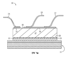
도 7은 본 발명의 다른 실시예에 따른, 와이어 본드가 통합된 도 6의 POL 구조들 중 하나의 개략적인 측부 단면도이다.
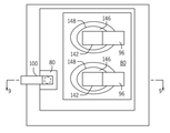
도 8 및 도 9는 본 발명의 다른 실시예에 따른, 와이어 본드를 갖는 POL 구조의 개략적인 상부도 및 측부 단면도이다.
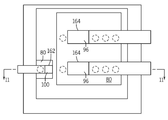
도 10 및 도 11은 본 발명의 또 다른 실시예에 따른, 와이어 본드를 갖는 POL 구조의 개략적인 상부도 및 측부 단면도이다.
도 12는 본 발명의 실시예에 따른, POL 구조가 통합된 재구성된 웨이퍼를 도시하는 개략적인 측부 단면도이다.
도 13은 본 발명의 다른 실시예에 따른, POL 구조가 통합된 재구성 된 웨이퍼를 도시하는 개략적인 측부 단면도이다.
도 14는 본 발명의 실시예에 따른, POL 조립체의 개략적인 측부 단면도이다.
도 15는 본 발명의 다른 실시예에 따른, POL 조립체의 개략적인 측부 단면도이다.
38: 반도체 디바이스
80: 금속 경로
84, 86: 금속 상호 연결
96, 98, 100: 와이어 본드
90, 92, 94: 개별 POL 구조
128: 콘택 표면
Claims (23)
- 파워 오버레이(POL) 구조로서,
파워 디바이스의 상부면 상에 배치되는 적어도 하나의 상부 콘택 패드를 갖는 파워 디바이스와,
상기 파워 디바이스의 상부면과 결합되는 유전체층 및 상기 유전체층을 통하여 형성되는 비아들을 통해 연장되고 상기 파워 디바이스의 상기 적어도 하나의 상부 콘택 패드와 전기적으로 결합되는 금속 상호 연결을 갖는 금속층을 포함하는 POL 상호 연결층과,
상기 금속층에 직접 결합되는 적어도 하나의 구리 와이어 본드를 포함하는 것인 POL 구조. - 제 1 항에 있어서,
상기 적어도 하나의 상부 콘택 패드는 알루미늄을 포함하는 것인 POL 구조. - 제 1 항에 있어서,
솔더층과 함께 상기 파워 디바이스의 하부 콘택 패드와 열적으로 또한 전기적으로 결합되는 다층 기판을 더 포함하며, 상기 다층 기판은 직접 본드 구리(DBC)와 직접 본드 알루미늄(DBA) 기판 중 하나를 포함하는 것인 POL 구조. - 제 1 항에 있어서,
상기 유전체층은 상기 적어도 하나의 구리 와이어 본드의 콘택 위치 아래에서 실질적으로 균일한 두께를 갖는 것인 POL 구조. - 제 1 항에 있어서,
상기 유전체층은 접착제층을 통해 상기 파워 디바이스의 상부면과 결합되는 것인 POL 구조. - 제 1 항에 있어서,
상기 와이어 본드의 콘택 표면과 상기 파워 디바이스 사이에 배치되는 POL 상호 연결층의 일부는 상기 유전체층을 갖지 않는 것인 POL 구조. - 제 1 항에 있어서,
상기 금속층의 상부면 아래에 위치되는 상부 콘택 표면을 갖는 금속 상호 연결과,
상기 금속 상호 연결의 상부 콘택 표면에 결합되는 구리 와이어 본드를 더 포함하고,
상기 상부 와이어 본드의 콘택 표면의 표면 영역은 상기 금속 상호 연결의 상부 콘택 표면의 표면 영역보다 작은 것인 POL 구조. - 제 1 항에 있어서,
상기 적어도 하나의 와이어 본드의 콘택 표면은 금속 상호 연결을 갖는 상기 POL 상호 연결층의 일부와 결합되는 것인 POL 구조. - 파워 오버레이(POL) 구조를 제조하는 방법으로서,
복수의 반도체 디바이스들을 포함하는 웨이퍼를 제공하는 단계와,
상기 복수의 반도체 디바이스들의 각각의 상부면과 유전체층을 결합하는 단계와,
상기 복수의 반도체 디바이스들 중 적어도 하나의 콘택 패드를 노출시키기 위해 상기 유전체층을 통해 복수의 비아들을 형성하는 단계와,
상기 유전체층의 상부면 상에 금속층을 형성하는 단계와,
상기 금속층의 상부 표면과 적어도 하나의 와이어 본드를 결합하는 단계를 포함하며,
상기 금속층은 상기 복수의 비아들을 통해 연장되며 상기 복수의 반도체 디바이스들 중 적어도 하나의 콘택 패드와 전기적으로 결합되는 금속 상호 연결을 갖는 것인 POL 구조 제조 방법. - 제 9 항에 있어서,
상기 복수의 반도체 디바이스들 각각의 상기 상부면과 유전체층을 결합하는 단계는 그들 사이에 접착제층을 배치하는 것을 포함하는 것인 POL 구조 제조 방법. - 제 9 항에 있어서,
상기 웨이퍼를 복수의 POL 구조들로 개별화(singulating)하는 단계를 더 포함하며, 상기 복수의 POL 구조들 각각은 유전체층의 일부와 그 위에 형성되는 금속층의 일부를 갖는 적어도 하나의 반도체 디바이스를 포함하는 것인 POL 구조 제조 방법. - 제 9 항에 있어서,
적어도 하나의 와이어 본드의 표면 영역보다 큰 콘택 패드의 표면 영역을 노출시키도록 비아를 형성하는 단계와,
상기 비아 내에 형성되는 금속 상호 연결과 적어도 하나의 와이어 본드를 결합하는 단계를 더 포함하는 것인 POL 구조 제조 방법. - 제 9 항에 있어서,
금속 상호 연결들이 없는 상기 금속층의 일부와 적어도 하나의 와이어 본드를 결합하는 단계를 더 포함하는 것인 POL 구조 제조 방법. - 제 9 항에 있어서,
상기 복수의 반도체 디바이스들의 상부면과 상기 유전체층을 결합하는 단계에 앞서, 상기 복수의 반도체 디바이스들의 하부면과 제거 가능한 지지 구조를 결합하는 단계를 더 포함하는 것인 POL 구조 제조 방법. - 제 9 항에 있어서,
상기 유전체층과 웨이퍼의 제 1 반도체 디바이스 및 제 2 반도체 디바이스를 결합하는 단계를 더 포함하며, 상기 제 1 반도체 디바이스는 상기 제 2 반도체 디바이스의 두께보다 큰 두께를 갖는 것인 POL 구조 제조 방법. - 제 15 항에 있어서,
상기 제 1 반도체 디바이스와 상기 제 2 반도체 사이에 갭이 형성되도록, 상기 제 1 반도체 디바이스를 상기 제 2 반도체 디바이스와 거리를 두어 위치시키는 단계를 더 포함하는 것인 POL 구조 제조 방법. - 제 15 항에 있어서,
상기 제 1 반도체 디바이스의 상부면이 상기 제 2 반도체 디바이스의 상부면과 실질적으로 동일 평면이 되도록, 상기 지지 구조와 상기 제 2 반도체 디바이스의 하부면 사이에 심(shim)을 배치하는 단계를 더 포함하는 것인 POL 구조 제조 방법. - 제 15 항에 있어서,
상기 제 1 반도체 디바이스와 상기 유전체층의 제 1 부분을 결합하는 단계와,
상기 제 2 반도체 디바이스와 상기 유전체층의 제 2 부분을 결합하는 단계를 더 포함하고,
상기 유전체층의 제 2 부분의 두께는 상기 유전체층의 제 1 부분의 두께보다 큰 것인 POL 구조 제조 방법. - 파워 오버레이(POL) 조립체로서,
제 1 반도체 디바이스 및 제 2 반도체 디바이스와,
상기 제 1 및 제 2 반도체 디바이스들의 상부 콘택 패드와 접착식으로 결합되는 폴리이미드 필름 및 상기 폴리이미드 필름 상에 형성되는 금속 경로를 포함하는 POL 상호 연결 조립체와,
상기 금속 경로와 직접 결합되는 복수의 구리 와이어 본드들을 포함하며,
상기 금속 경로는 상기 폴리이미드 필름을 통해 형성되는 비아들을 통해 연장되며 상기 제 1 및 제 2 반도체 디바이스들의 상부 콘택 패드들과 전기적으로 결합되는 복수의 금속 상호 연결을 포함하며,
상기 복수의 구리 와이어 본드들 중 제 1 와이어 본드는 상기 제 1 반도체 디바이스의 상부 콘택 패드와 전기적으로 결합되고,
상기 복수의 구리 와이어 본드들 중 제 2 와이어 본드는 상기 제 2 반도체 디바이스의 상부 콘택 패드와 전기적으로 결합되는 것인 POL 조립체. - 제 19 항에 있어서,
상기 제 1 POL 구조 중 적어도 하나의 구리 와이어 본드는 상기 제 2 POL 구조 중 적어도 하나의 구리 와이어 본드와 전기적으로 결합되는 것인 POL 조립체. - 제 19 항에 있어서,
상기 제 1 반도체 디바이스의 두께는 상기 제 2 반도체 디바이스의 두께와 다르고,
상기 POL 조립체는 가변 두께를 갖는 폴리이미드 필름과, 상기 제 1 및 제 2 반도체 디바이스들 중 하나의 하부면과 결합되는 심 중 적어도 하나를 포함하는 것인 POL 조립체. - 제 19 항에 있어서,
상기 제 1 와이어 본드는 실질적으로 폴리이미드 필름이 없는 상기 POL 상호 연결 조립체의 일부와 결합되는 것인 POL 조립체. - 제 19 항에 있어서,
상기 제 1 와이어 본드는 상기 POL 상호 연결 조립체의 일부와 결합되며, 상기 폴리이미드 필름은 실질적으로 균일한 두께를 갖는 것인 POL 조립체.
Applications Claiming Priority (2)
| Application Number | Priority Date | Filing Date | Title |
|---|---|---|---|
| US14/512,562 US9613843B2 (en) | 2014-10-13 | 2014-10-13 | Power overlay structure having wirebonds and method of manufacturing same |
| US14/512,562 | 2014-10-13 |
Publications (2)
| Publication Number | Publication Date |
|---|---|
| KR20160043518A true KR20160043518A (ko) | 2016-04-21 |
| KR102419302B1 KR102419302B1 (ko) | 2022-07-12 |
Family
ID=54293117
Family Applications (1)
| Application Number | Title | Priority Date | Filing Date |
|---|---|---|---|
| KR1020150142769A Active KR102419302B1 (ko) | 2014-10-13 | 2015-10-13 | 와이어 본드를 갖는 파워 오버레이 구조 및 그 제조 방법 |
Country Status (6)
| Country | Link |
|---|---|
| US (2) | US9613843B2 (ko) |
| EP (1) | EP3010038A3 (ko) |
| JP (3) | JP2016082230A (ko) |
| KR (1) | KR102419302B1 (ko) |
| CN (3) | CN116544208A (ko) |
| TW (1) | TWI713470B (ko) |
Cited By (1)
| Publication number | Priority date | Publication date | Assignee | Title |
|---|---|---|---|---|
| USD881189S1 (en) | 2018-02-26 | 2020-04-14 | Samsung Electronics Co., Ltd. | Head-mounted display device |
Families Citing this family (21)
| Publication number | Priority date | Publication date | Assignee | Title |
|---|---|---|---|---|
| US9613843B2 (en) * | 2014-10-13 | 2017-04-04 | General Electric Company | Power overlay structure having wirebonds and method of manufacturing same |
| DE102015102535B4 (de) * | 2015-02-23 | 2023-08-03 | Infineon Technologies Ag | Verbundsystem und Verfahren zum haftenden Verbinden eines hygroskopischen Materials |
| US10056319B2 (en) * | 2016-04-29 | 2018-08-21 | Delta Electronics, Inc. | Power module package having patterned insulation metal substrate |
| JP6726112B2 (ja) * | 2017-01-19 | 2020-07-22 | 株式会社 日立パワーデバイス | 半導体装置および電力変換装置 |
| JP7163054B2 (ja) * | 2017-04-20 | 2022-10-31 | ローム株式会社 | 半導体装置 |
| US10541209B2 (en) | 2017-08-03 | 2020-01-21 | General Electric Company | Electronics package including integrated electromagnetic interference shield and method of manufacturing thereof |
| US10541153B2 (en) | 2017-08-03 | 2020-01-21 | General Electric Company | Electronics package with integrated interconnect structure and method of manufacturing thereof |
| US10804115B2 (en) | 2017-08-03 | 2020-10-13 | General Electric Company | Electronics package with integrated interconnect structure and method of manufacturing thereof |
| US10332832B2 (en) | 2017-08-07 | 2019-06-25 | General Electric Company | Method of manufacturing an electronics package using device-last or device-almost last placement |
| US10957832B2 (en) | 2018-10-22 | 2021-03-23 | General Electric Company | Electronics package for light emitting semiconductor devices and method of manufacturing thereof |
| US11538769B2 (en) * | 2018-12-14 | 2022-12-27 | General Electric Company | High voltage semiconductor devices having improved electric field suppression |
| US10892237B2 (en) * | 2018-12-14 | 2021-01-12 | General Electric Company | Methods of fabricating high voltage semiconductor devices having improved electric field suppression |
| JP7472435B2 (ja) | 2019-05-13 | 2024-04-23 | 富士電機株式会社 | 半導体モジュールの製造方法 |
| CN111162015A (zh) * | 2019-12-20 | 2020-05-15 | 珠海格力电器股份有限公司 | 一种智能功率模块及封装方法 |
| US11776870B2 (en) * | 2020-01-16 | 2023-10-03 | Semiconductor Components Industries, Llc | Direct bonded copper substrates fabricated using silver sintering |
| US11398445B2 (en) | 2020-05-29 | 2022-07-26 | General Electric Company | Mechanical punched via formation in electronics package and electronics package formed thereby |
| WO2022029828A1 (ja) * | 2020-08-03 | 2022-02-10 | 三菱電機株式会社 | 半導体装置、半導体装置の製造方法および電力変換装置 |
| EP4012753A1 (en) * | 2020-12-08 | 2022-06-15 | Hitachi Energy Switzerland AG | Semiconductor device, semiconductor module and manufacturing method |
| CN112910285B (zh) * | 2021-01-05 | 2022-06-14 | 深圳市富鑫产业科技有限公司 | 一种逆变器电力系统及其制造方法 |
| US11848244B2 (en) * | 2021-09-30 | 2023-12-19 | Texas Instruments Incorporated | Leaded wafer chip scale packages |
| WO2026009326A1 (ja) * | 2024-07-02 | 2026-01-08 | 三菱電機株式会社 | 半導体装置及び電力変換装置 |
Citations (4)
| Publication number | Priority date | Publication date | Assignee | Title |
|---|---|---|---|---|
| JPH0933940A (ja) * | 1995-07-14 | 1997-02-07 | Citizen Watch Co Ltd | 表示パネル駆動用半導体チップの実装構造 |
| JP2006165515A (ja) * | 2004-11-11 | 2006-06-22 | Denso Corp | 半導体装置およびその製造方法 |
| US20140001615A1 (en) * | 2012-06-27 | 2014-01-02 | Infineon Technologies Austria Ag | Package-In-Packages and Methods of Formation Thereof |
| US20140167248A1 (en) * | 2012-12-19 | 2014-06-19 | General Electric Company | Power module package |
Family Cites Families (61)
| Publication number | Priority date | Publication date | Assignee | Title |
|---|---|---|---|---|
| FR2599893B1 (fr) * | 1986-05-23 | 1996-08-02 | Ricoh Kk | Procede de montage d'un module electronique sur un substrat et carte a circuit integre |
| EP0646959B1 (en) * | 1993-09-30 | 2001-08-16 | Consorzio per la Ricerca sulla Microelettronica nel Mezzogiorno | Metallization and bonding process for manufacturing power semiconductor devices |
| US5637922A (en) * | 1994-02-07 | 1997-06-10 | General Electric Company | Wireless radio frequency power semiconductor devices using high density interconnect |
| JP3432284B2 (ja) * | 1994-07-04 | 2003-08-04 | 三菱電機株式会社 | 半導体装置 |
| JPH08213420A (ja) * | 1995-02-03 | 1996-08-20 | Hitachi Ltd | 半導体装置 |
| DE19612838A1 (de) * | 1995-11-13 | 1997-05-15 | Asea Brown Boveri | Leistungshalbleiterbauelement sowie Verfahren zu dessen Herstellung |
| JP3415981B2 (ja) * | 1996-01-10 | 2003-06-09 | 株式会社日立製作所 | 半導体装置、その製造方法、および表面保護膜 |
| US6057612A (en) * | 1998-07-02 | 2000-05-02 | Intersil Corporation | Flat power pack |
| US6440641B1 (en) * | 1998-07-31 | 2002-08-27 | Kulicke & Soffa Holdings, Inc. | Deposited thin film build-up layer dimensions as a method of relieving stress in high density interconnect printed wiring board substrates |
| US6232151B1 (en) * | 1999-11-01 | 2001-05-15 | General Electric Company | Power electronic module packaging |
| EP1139413B1 (en) | 2000-03-24 | 2005-03-16 | Texas Instruments Incorporated | Wire bonding process |
| FR2822591A1 (fr) * | 2001-03-22 | 2002-09-27 | Commissariat Energie Atomique | Assemblage de composants d'epaisseurs diverses |
| JP3719994B2 (ja) * | 2001-12-28 | 2005-11-24 | 株式会社東芝 | 半導体装置 |
| JP2003347741A (ja) * | 2002-05-30 | 2003-12-05 | Taiyo Yuden Co Ltd | 複合多層基板およびそれを用いたモジュール |
| US6979891B2 (en) * | 2003-09-08 | 2005-12-27 | Intel Corporation | Integrated circuit packaging architecture |
| US6995475B2 (en) * | 2003-09-18 | 2006-02-07 | International Business Machines Corporation | I/C chip suitable for wire bonding |
| FI117814B (fi) * | 2004-06-15 | 2007-02-28 | Imbera Electronics Oy | Menetelmä elektroniikkamoduulin valmistamiseksi |
| DE102004043020B3 (de) | 2004-09-06 | 2006-04-27 | eupec Europäische Gesellschaft für Leistungshalbleiter mbH | Bonddraht und Bondverbindung |
| US7327024B2 (en) * | 2004-11-24 | 2008-02-05 | General Electric Company | Power module, and phase leg assembly |
| JP4710700B2 (ja) * | 2005-05-09 | 2011-06-29 | 株式会社デンソー | 半導体装置およびその製造方法 |
| JP2007073611A (ja) * | 2005-09-05 | 2007-03-22 | Renesas Technology Corp | 電子装置およびその製造方法 |
| JP2007109932A (ja) * | 2005-10-14 | 2007-04-26 | Toshiba Corp | 半導体装置 |
| US8164176B2 (en) * | 2006-10-20 | 2012-04-24 | Infineon Technologies Ag | Semiconductor module arrangement |
| US20080190748A1 (en) * | 2007-02-13 | 2008-08-14 | Stephen Daley Arthur | Power overlay structure for mems devices and method for making power overlay structure for mems devices |
| US7884452B2 (en) * | 2007-11-23 | 2011-02-08 | Alpha And Omega Semiconductor Incorporated | Semiconductor power device package having a lead frame-based integrated inductor |
| US8039302B2 (en) * | 2007-12-07 | 2011-10-18 | Stats Chippac, Ltd. | Semiconductor package and method of forming similar structure for top and bottom bonding pads |
| US7947592B2 (en) * | 2007-12-14 | 2011-05-24 | Semiconductor Components Industries, Llc | Thick metal interconnect with metal pad caps at selective sites and process for making the same |
| US7960845B2 (en) | 2008-01-03 | 2011-06-14 | Linear Technology Corporation | Flexible contactless wire bonding structure and methodology for semiconductor device |
| US7839642B2 (en) * | 2008-04-04 | 2010-11-23 | Liebert Corporation | Heat-sink brace for fault-force support |
| JP5331610B2 (ja) * | 2008-12-03 | 2013-10-30 | ルネサスエレクトロニクス株式会社 | 半導体集積回路装置 |
| US9064936B2 (en) * | 2008-12-12 | 2015-06-23 | Stats Chippac, Ltd. | Semiconductor device and method of forming a vertical interconnect structure for 3-D FO-WLCSP |
| US8592992B2 (en) * | 2011-12-14 | 2013-11-26 | Stats Chippac, Ltd. | Semiconductor device and method of forming vertical interconnect structure with conductive micro via array for 3-D Fo-WLCSP |
| US7915741B2 (en) * | 2009-02-24 | 2011-03-29 | Unisem Advanced Technologies Sdn. Bhd. | Solder bump UBM structure |
| US8358000B2 (en) * | 2009-03-13 | 2013-01-22 | General Electric Company | Double side cooled power module with power overlay |
| TW201113993A (en) * | 2009-10-01 | 2011-04-16 | Anpec Electronics Corp | Pre-packaged structure |
| EP2328172B1 (en) | 2009-10-02 | 2019-06-26 | Abb Research Ltd. | A power-electronic arrangement |
| US8242013B2 (en) * | 2010-03-30 | 2012-08-14 | Alpha & Omega Semiconductor Inc. | Virtually substrate-less composite power semiconductor device and method |
| JP2011222555A (ja) * | 2010-04-02 | 2011-11-04 | Denso Corp | 半導体チップ内蔵配線基板の製造方法 |
| JP5568357B2 (ja) * | 2010-04-05 | 2014-08-06 | 株式会社フジクラ | 半導体装置及びその製造方法 |
| US8531027B2 (en) * | 2010-04-30 | 2013-09-10 | General Electric Company | Press-pack module with power overlay interconnection |
| JP5607994B2 (ja) * | 2010-06-15 | 2014-10-15 | ルネサスエレクトロニクス株式会社 | 半導体集積回路装置およびその製造方法 |
| US8114712B1 (en) * | 2010-12-22 | 2012-02-14 | General Electric Company | Method for fabricating a semiconductor device package |
| US10204879B2 (en) * | 2011-01-21 | 2019-02-12 | STATS ChipPAC Pte. Ltd. | Semiconductor device and method of forming wafer-level interconnect structures with advanced dielectric characteristics |
| EP2482312A4 (en) * | 2011-04-29 | 2012-09-26 | Huawei Tech Co Ltd | POWER SUPPLY MODULE AND PACKAGING AND INTEGRATION METHOD THEREFOR |
| TWI489601B (zh) * | 2011-05-03 | 2015-06-21 | 財團法人工業技術研究院 | 電子元件封裝結構 |
| US8653635B2 (en) * | 2011-08-16 | 2014-02-18 | General Electric Company | Power overlay structure with leadframe connections |
| US9066443B2 (en) * | 2011-09-13 | 2015-06-23 | General Electric Company | Overlay circuit structure for interconnecting light emitting semiconductors |
| US9385009B2 (en) * | 2011-09-23 | 2016-07-05 | STATS ChipPAC Pte. Ltd. | Semiconductor device and method of forming stacked vias within interconnect structure for Fo-WLCSP |
| US20130154099A1 (en) | 2011-12-16 | 2013-06-20 | Semiconductor Components Industries, Llc | Pad over interconnect pad structure design |
| US8716870B2 (en) * | 2011-12-16 | 2014-05-06 | General Electric Company | Direct write interconnections and method of manufacturing thereof |
| US8907467B2 (en) * | 2012-03-28 | 2014-12-09 | Infineon Technologies Ag | PCB based RF-power package window frame |
| US9337163B2 (en) * | 2012-11-13 | 2016-05-10 | General Electric Company | Low profile surface mount package with isolated tab |
| US8987876B2 (en) | 2013-03-14 | 2015-03-24 | General Electric Company | Power overlay structure and method of making same |
| US10418298B2 (en) * | 2013-09-24 | 2019-09-17 | STATS ChipPAC Pte. Ltd. | Semiconductor device and method of forming dual fan-out semiconductor package |
| US9806051B2 (en) * | 2014-03-04 | 2017-10-31 | General Electric Company | Ultra-thin embedded semiconductor device package and method of manufacturing thereof |
| US10804153B2 (en) * | 2014-06-16 | 2020-10-13 | STATS ChipPAC Pte. Ltd. | Semiconductor device and method to minimize stress on stack via |
| US9978700B2 (en) * | 2014-06-16 | 2018-05-22 | STATS ChipPAC Pte. Ltd. | Method for building up a fan-out RDL structure with fine pitch line-width and line-spacing |
| US20150364430A1 (en) * | 2014-06-16 | 2015-12-17 | Stats Chippac, Ltd. | Semiconductor Device and Method of Forming a Dampening Structure to Improve Board Level Reliability |
| US9613843B2 (en) * | 2014-10-13 | 2017-04-04 | General Electric Company | Power overlay structure having wirebonds and method of manufacturing same |
| US9941207B2 (en) * | 2014-10-24 | 2018-04-10 | STATS ChipPAC Pte. Ltd. | Semiconductor device and method of fabricating 3D package with short cycle time and high yield |
| US10453786B2 (en) * | 2016-01-19 | 2019-10-22 | General Electric Company | Power electronics package and method of manufacturing thereof |
-
2014
- 2014-10-13 US US14/512,562 patent/US9613843B2/en active Active
-
2015
- 2015-10-07 TW TW104133047A patent/TWI713470B/zh active
- 2015-10-07 JP JP2015198983A patent/JP2016082230A/ja active Pending
- 2015-10-12 EP EP15189400.3A patent/EP3010038A3/en active Pending
- 2015-10-13 CN CN202310295935.6A patent/CN116544208A/zh active Pending
- 2015-10-13 CN CN202010112037.9A patent/CN111508856B/zh active Active
- 2015-10-13 CN CN201510668963.3A patent/CN105514077B/zh active Active
- 2015-10-13 KR KR1020150142769A patent/KR102419302B1/ko active Active
-
2017
- 2017-03-29 US US15/472,912 patent/US10204881B2/en active Active
-
2021
- 2021-01-22 JP JP2021008342A patent/JP7254840B2/ja active Active
-
2023
- 2023-03-28 JP JP2023052419A patent/JP7704383B2/ja active Active
Patent Citations (4)
| Publication number | Priority date | Publication date | Assignee | Title |
|---|---|---|---|---|
| JPH0933940A (ja) * | 1995-07-14 | 1997-02-07 | Citizen Watch Co Ltd | 表示パネル駆動用半導体チップの実装構造 |
| JP2006165515A (ja) * | 2004-11-11 | 2006-06-22 | Denso Corp | 半導体装置およびその製造方法 |
| US20140001615A1 (en) * | 2012-06-27 | 2014-01-02 | Infineon Technologies Austria Ag | Package-In-Packages and Methods of Formation Thereof |
| US20140167248A1 (en) * | 2012-12-19 | 2014-06-19 | General Electric Company | Power module package |
Cited By (1)
| Publication number | Priority date | Publication date | Assignee | Title |
|---|---|---|---|---|
| USD881189S1 (en) | 2018-02-26 | 2020-04-14 | Samsung Electronics Co., Ltd. | Head-mounted display device |
Also Published As
| Publication number | Publication date |
|---|---|
| JP7254840B2 (ja) | 2023-04-10 |
| JP2021061453A (ja) | 2021-04-15 |
| JP2023078435A (ja) | 2023-06-06 |
| CN111508856B (zh) | 2023-03-21 |
| US9613843B2 (en) | 2017-04-04 |
| TW201626468A (zh) | 2016-07-16 |
| CN116544208A (zh) | 2023-08-04 |
| US10204881B2 (en) | 2019-02-12 |
| CN105514077A (zh) | 2016-04-20 |
| JP7704383B2 (ja) | 2025-07-08 |
| CN105514077B (zh) | 2020-03-31 |
| US20170200692A1 (en) | 2017-07-13 |
| US20160104666A1 (en) | 2016-04-14 |
| TWI713470B (zh) | 2020-12-21 |
| JP2016082230A (ja) | 2016-05-16 |
| EP3010038A3 (en) | 2016-07-20 |
| CN111508856A (zh) | 2020-08-07 |
| EP3010038A2 (en) | 2016-04-20 |
| KR102419302B1 (ko) | 2022-07-12 |
Similar Documents
| Publication | Publication Date | Title |
|---|---|---|
| JP7254840B2 (ja) | ワイヤボンドを有するパワーオーバーレイ構造体およびその製造方法 | |
| KR101353927B1 (ko) | 얇은 다이들 및 금속 기판들을 사용하는 반도체 다이 패키지들 | |
| US9704788B2 (en) | Power overlay structure and method of making same | |
| US10312194B2 (en) | Stacked electronics package and method of manufacturing thereof | |
| US12094807B2 (en) | Stacked transistor chip package with source coupling | |
| US10332832B2 (en) | Method of manufacturing an electronics package using device-last or device-almost last placement | |
| US10770444B2 (en) | Electronics package having a multi-thickness conductor layer and method of manufacturing thereof | |
| US10700035B2 (en) | Stacked electronics package and method of manufacturing thereof | |
| KR20160115861A (ko) | 리드프레임 상의 기판 인터포저 | |
| CN117043941A (zh) | 具有多个顶侧连接的双侧芯片堆叠组合件 | |
| US20240404958A1 (en) | Power module package and manufacture method thereof | |
| Essig et al. | High efficient mid power modules by next generation chip embedding technology | |
| WO2025258270A1 (ja) | 半導体装置 |
Legal Events
| Date | Code | Title | Description |
|---|---|---|---|
| PA0109 | Patent application |
St.27 status event code: A-0-1-A10-A12-nap-PA0109 |
|
| PG1501 | Laying open of application |
St.27 status event code: A-1-1-Q10-Q12-nap-PG1501 |
|
| P22-X000 | Classification modified |
St.27 status event code: A-2-2-P10-P22-nap-X000 |
|
| A201 | Request for examination | ||
| PA0201 | Request for examination |
St.27 status event code: A-1-2-D10-D11-exm-PA0201 |
|
| D13-X000 | Search requested |
St.27 status event code: A-1-2-D10-D13-srh-X000 |
|
| D14-X000 | Search report completed |
St.27 status event code: A-1-2-D10-D14-srh-X000 |
|
| E902 | Notification of reason for refusal | ||
| PE0902 | Notice of grounds for rejection |
St.27 status event code: A-1-2-D10-D21-exm-PE0902 |
|
| P11-X000 | Amendment of application requested |
St.27 status event code: A-2-2-P10-P11-nap-X000 |
|
| P13-X000 | Application amended |
St.27 status event code: A-2-2-P10-P13-nap-X000 |
|
| E701 | Decision to grant or registration of patent right | ||
| PE0701 | Decision of registration |
St.27 status event code: A-1-2-D10-D22-exm-PE0701 |
|
| GRNT | Written decision to grant | ||
| PR0701 | Registration of establishment |
St.27 status event code: A-2-4-F10-F11-exm-PR0701 |
|
| PR1002 | Payment of registration fee |
St.27 status event code: A-2-2-U10-U11-oth-PR1002 Fee payment year number: 1 |
|
| PG1601 | Publication of registration |
St.27 status event code: A-4-4-Q10-Q13-nap-PG1601 |
|
| PR1001 | Payment of annual fee |
St.27 status event code: A-4-4-U10-U11-oth-PR1001 Fee payment year number: 4 |
|
| R18 | Changes to party contact information recorded |
Free format text: ST27 STATUS EVENT CODE: A-5-5-R10-R18-OTH-X000 (AS PROVIDED BY THE NATIONAL OFFICE) |
|
| R18-X000 | Changes to party contact information recorded |
St.27 status event code: A-5-5-R10-R18-oth-X000 |
|
| P22-X000 | Classification modified |
St.27 status event code: A-4-4-P10-P22-nap-X000 |