KR20170091760A - 반도체 장치 - Google Patents
반도체 장치 Download PDFInfo
- Publication number
- KR20170091760A KR20170091760A KR1020177021208A KR20177021208A KR20170091760A KR 20170091760 A KR20170091760 A KR 20170091760A KR 1020177021208 A KR1020177021208 A KR 1020177021208A KR 20177021208 A KR20177021208 A KR 20177021208A KR 20170091760 A KR20170091760 A KR 20170091760A
- Authority
- KR
- South Korea
- Prior art keywords
- layer
- oxide semiconductor
- oxide
- insulating layer
- electrode layer
- Prior art date
- Legal status (The legal status is an assumption and is not a legal conclusion. Google has not performed a legal analysis and makes no representation as to the accuracy of the status listed.)
- Ceased
Links
- 239000004065 semiconductor Substances 0.000 title claims abstract description 267
- 239000010410 layer Substances 0.000 claims description 421
- 238000000034 method Methods 0.000 claims description 43
- VYPSYNLAJGMNEJ-UHFFFAOYSA-N Silicium dioxide Chemical compound O=[Si]=O VYPSYNLAJGMNEJ-UHFFFAOYSA-N 0.000 claims description 41
- XUIMIQQOPSSXEZ-UHFFFAOYSA-N Silicon Chemical compound [Si] XUIMIQQOPSSXEZ-UHFFFAOYSA-N 0.000 claims description 38
- 229910052710 silicon Inorganic materials 0.000 claims description 38
- 239000010703 silicon Substances 0.000 claims description 38
- 229910052814 silicon oxide Inorganic materials 0.000 claims description 35
- 229910052581 Si3N4 Inorganic materials 0.000 claims description 31
- HQVNEWCFYHHQES-UHFFFAOYSA-N silicon nitride Chemical compound N12[Si]34N5[Si]62N3[Si]51N64 HQVNEWCFYHHQES-UHFFFAOYSA-N 0.000 claims description 31
- 229910052782 aluminium Inorganic materials 0.000 claims description 26
- XAGFODPZIPBFFR-UHFFFAOYSA-N aluminium Chemical compound [Al] XAGFODPZIPBFFR-UHFFFAOYSA-N 0.000 claims description 22
- 239000010936 titanium Substances 0.000 claims description 21
- RTAQQCXQSZGOHL-UHFFFAOYSA-N Titanium Chemical compound [Ti] RTAQQCXQSZGOHL-UHFFFAOYSA-N 0.000 claims description 20
- 229910052719 titanium Inorganic materials 0.000 claims description 20
- WFKWXMTUELFFGS-UHFFFAOYSA-N tungsten Chemical compound [W] WFKWXMTUELFFGS-UHFFFAOYSA-N 0.000 claims description 17
- 229910052721 tungsten Inorganic materials 0.000 claims description 17
- 239000010937 tungsten Substances 0.000 claims description 17
- 229910052751 metal Inorganic materials 0.000 claims description 16
- 239000002184 metal Substances 0.000 claims description 14
- ZOKXTWBITQBERF-UHFFFAOYSA-N Molybdenum Chemical compound [Mo] ZOKXTWBITQBERF-UHFFFAOYSA-N 0.000 claims description 13
- 229910052750 molybdenum Inorganic materials 0.000 claims description 13
- 239000011733 molybdenum Substances 0.000 claims description 13
- VYZAMTAEIAYCRO-UHFFFAOYSA-N Chromium Chemical compound [Cr] VYZAMTAEIAYCRO-UHFFFAOYSA-N 0.000 claims description 12
- 229910052804 chromium Inorganic materials 0.000 claims description 12
- 239000011651 chromium Substances 0.000 claims description 12
- 229910052715 tantalum Inorganic materials 0.000 claims description 12
- GUVRBAGPIYLISA-UHFFFAOYSA-N tantalum atom Chemical compound [Ta] GUVRBAGPIYLISA-UHFFFAOYSA-N 0.000 claims description 12
- 229910052733 gallium Inorganic materials 0.000 claims description 11
- 229910052779 Neodymium Inorganic materials 0.000 claims description 9
- QEFYFXOXNSNQGX-UHFFFAOYSA-N neodymium atom Chemical compound [Nd] QEFYFXOXNSNQGX-UHFFFAOYSA-N 0.000 claims description 9
- RYGMFSIKBFXOCR-UHFFFAOYSA-N Copper Chemical compound [Cu] RYGMFSIKBFXOCR-UHFFFAOYSA-N 0.000 claims description 8
- 229910052802 copper Inorganic materials 0.000 claims description 8
- 239000010949 copper Substances 0.000 claims description 8
- 229910045601 alloy Inorganic materials 0.000 claims description 7
- 239000000956 alloy Substances 0.000 claims description 7
- 239000013078 crystal Substances 0.000 claims description 7
- TWNQGVIAIRXVLR-UHFFFAOYSA-N oxo(oxoalumanyloxy)alumane Chemical compound O=[Al]O[Al]=O TWNQGVIAIRXVLR-UHFFFAOYSA-N 0.000 claims description 7
- 229910052706 scandium Inorganic materials 0.000 claims description 6
- SIXSYDAISGFNSX-UHFFFAOYSA-N scandium atom Chemical compound [Sc] SIXSYDAISGFNSX-UHFFFAOYSA-N 0.000 claims description 6
- 239000002356 single layer Substances 0.000 claims description 6
- 229910052738 indium Inorganic materials 0.000 claims description 5
- 229910052725 zinc Inorganic materials 0.000 claims description 5
- 239000011701 zinc Substances 0.000 claims description 5
- GYHNNYVSQQEPJS-UHFFFAOYSA-N Gallium Chemical compound [Ga] GYHNNYVSQQEPJS-UHFFFAOYSA-N 0.000 claims description 4
- HCHKCACWOHOZIP-UHFFFAOYSA-N Zinc Chemical compound [Zn] HCHKCACWOHOZIP-UHFFFAOYSA-N 0.000 claims description 4
- 229910000449 hafnium oxide Inorganic materials 0.000 claims description 4
- WIHZLLGSGQNAGK-UHFFFAOYSA-N hafnium(4+);oxygen(2-) Chemical compound [O-2].[O-2].[Hf+4] WIHZLLGSGQNAGK-UHFFFAOYSA-N 0.000 claims description 4
- APFVFJFRJDLVQX-UHFFFAOYSA-N indium atom Chemical compound [In] APFVFJFRJDLVQX-UHFFFAOYSA-N 0.000 claims description 4
- BPUBBGLMJRNUCC-UHFFFAOYSA-N oxygen(2-);tantalum(5+) Chemical compound [O-2].[O-2].[O-2].[O-2].[O-2].[Ta+5].[Ta+5] BPUBBGLMJRNUCC-UHFFFAOYSA-N 0.000 claims description 2
- 229910001936 tantalum oxide Inorganic materials 0.000 claims description 2
- 239000005001 laminate film Substances 0.000 claims 1
- QVGXLLKOCUKJST-UHFFFAOYSA-N atomic oxygen Chemical compound [O] QVGXLLKOCUKJST-UHFFFAOYSA-N 0.000 abstract description 35
- 239000001301 oxygen Substances 0.000 abstract description 35
- 229910052760 oxygen Inorganic materials 0.000 abstract description 35
- 230000000694 effects Effects 0.000 abstract description 23
- 230000008859 change Effects 0.000 abstract description 11
- 238000006356 dehydrogenation reaction Methods 0.000 abstract description 10
- 230000007850 degeneration Effects 0.000 abstract 1
- 239000010408 film Substances 0.000 description 119
- 238000010438 heat treatment Methods 0.000 description 48
- 238000004544 sputter deposition Methods 0.000 description 43
- 239000000463 material Substances 0.000 description 40
- 239000000758 substrate Substances 0.000 description 38
- 239000007789 gas Substances 0.000 description 37
- XKRFYHLGVUSROY-UHFFFAOYSA-N Argon Chemical compound [Ar] XKRFYHLGVUSROY-UHFFFAOYSA-N 0.000 description 34
- 239000001257 hydrogen Substances 0.000 description 31
- 229910052739 hydrogen Inorganic materials 0.000 description 31
- 230000002829 reductive effect Effects 0.000 description 29
- 239000012535 impurity Substances 0.000 description 26
- UFHFLCQGNIYNRP-UHFFFAOYSA-N Hydrogen Chemical compound [H][H] UFHFLCQGNIYNRP-UHFFFAOYSA-N 0.000 description 23
- 229910007541 Zn O Inorganic materials 0.000 description 21
- 239000012298 atmosphere Substances 0.000 description 20
- 230000015572 biosynthetic process Effects 0.000 description 20
- XLOMVQKBTHCTTD-UHFFFAOYSA-N Zinc monoxide Chemical compound [Zn]=O XLOMVQKBTHCTTD-UHFFFAOYSA-N 0.000 description 18
- 230000006870 function Effects 0.000 description 18
- 229910052786 argon Inorganic materials 0.000 description 17
- IJGRMHOSHXDMSA-UHFFFAOYSA-N Atomic nitrogen Chemical compound N#N IJGRMHOSHXDMSA-UHFFFAOYSA-N 0.000 description 16
- 229910044991 metal oxide Inorganic materials 0.000 description 16
- 150000004706 metal oxides Chemical class 0.000 description 16
- XLYOFNOQVPJJNP-UHFFFAOYSA-N water Substances O XLYOFNOQVPJJNP-UHFFFAOYSA-N 0.000 description 16
- 238000010586 diagram Methods 0.000 description 13
- 238000004364 calculation method Methods 0.000 description 12
- 238000004519 manufacturing process Methods 0.000 description 12
- 238000005268 plasma chemical vapour deposition Methods 0.000 description 12
- 239000000969 carrier Substances 0.000 description 10
- 238000004891 communication Methods 0.000 description 10
- 239000011787 zinc oxide Substances 0.000 description 10
- 239000007769 metal material Substances 0.000 description 9
- 230000008569 process Effects 0.000 description 9
- GQPLMRYTRLFLPF-UHFFFAOYSA-N Nitrous Oxide Chemical compound [O-][N+]#N GQPLMRYTRLFLPF-UHFFFAOYSA-N 0.000 description 8
- 230000018044 dehydration Effects 0.000 description 8
- 238000006297 dehydration reaction Methods 0.000 description 8
- 230000005684 electric field Effects 0.000 description 8
- 239000011521 glass Substances 0.000 description 8
- 229910052757 nitrogen Inorganic materials 0.000 description 8
- 230000007547 defect Effects 0.000 description 7
- 238000000151 deposition Methods 0.000 description 7
- 150000002431 hydrogen Chemical class 0.000 description 7
- 239000011261 inert gas Substances 0.000 description 7
- 239000000370 acceptor Substances 0.000 description 6
- 230000008021 deposition Effects 0.000 description 6
- PJXISJQVUVHSOJ-UHFFFAOYSA-N indium(iii) oxide Chemical compound [O-2].[O-2].[O-2].[In+3].[In+3] PJXISJQVUVHSOJ-UHFFFAOYSA-N 0.000 description 6
- 239000012299 nitrogen atmosphere Substances 0.000 description 6
- 238000000206 photolithography Methods 0.000 description 6
- 239000010453 quartz Substances 0.000 description 6
- 238000004151 rapid thermal annealing Methods 0.000 description 6
- -1 that is Substances 0.000 description 6
- 230000004888 barrier function Effects 0.000 description 5
- 238000013461 design Methods 0.000 description 5
- 239000001307 helium Substances 0.000 description 5
- 229910052734 helium Inorganic materials 0.000 description 5
- SWQJXJOGLNCZEY-UHFFFAOYSA-N helium atom Chemical compound [He] SWQJXJOGLNCZEY-UHFFFAOYSA-N 0.000 description 5
- 239000000203 mixture Substances 0.000 description 5
- XOLBLPGZBRYERU-UHFFFAOYSA-N tin dioxide Chemical compound O=[Sn]=O XOLBLPGZBRYERU-UHFFFAOYSA-N 0.000 description 5
- 229910001887 tin oxide Inorganic materials 0.000 description 5
- 229910006404 SnO 2 Inorganic materials 0.000 description 4
- 238000000137 annealing Methods 0.000 description 4
- 125000004429 atom Chemical group 0.000 description 4
- PMHQVHHXPFUNSP-UHFFFAOYSA-M copper(1+);methylsulfanylmethane;bromide Chemical compound Br[Cu].CSC PMHQVHHXPFUNSP-UHFFFAOYSA-M 0.000 description 4
- 125000004435 hydrogen atom Chemical group [H]* 0.000 description 4
- 125000002887 hydroxy group Chemical group [H]O* 0.000 description 4
- 229910003437 indium oxide Inorganic materials 0.000 description 4
- 229910052748 manganese Inorganic materials 0.000 description 4
- 238000005259 measurement Methods 0.000 description 4
- 239000001272 nitrous oxide Substances 0.000 description 4
- 238000012545 processing Methods 0.000 description 4
- 230000001681 protective effect Effects 0.000 description 4
- 238000001552 radio frequency sputter deposition Methods 0.000 description 4
- 239000010409 thin film Substances 0.000 description 4
- 229910005191 Ga 2 O 3 Inorganic materials 0.000 description 3
- BLRPTPMANUNPDV-UHFFFAOYSA-N Silane Chemical compound [SiH4] BLRPTPMANUNPDV-UHFFFAOYSA-N 0.000 description 3
- 229910052799 carbon Inorganic materials 0.000 description 3
- 230000015556 catabolic process Effects 0.000 description 3
- 238000005229 chemical vapour deposition Methods 0.000 description 3
- 150000001875 compounds Chemical class 0.000 description 3
- 230000007423 decrease Effects 0.000 description 3
- 238000005530 etching Methods 0.000 description 3
- 238000011049 filling Methods 0.000 description 3
- 150000004678 hydrides Chemical class 0.000 description 3
- 238000003780 insertion Methods 0.000 description 3
- 230000037431 insertion Effects 0.000 description 3
- 238000003475 lamination Methods 0.000 description 3
- 229910052754 neon Inorganic materials 0.000 description 3
- GKAOGPIIYCISHV-UHFFFAOYSA-N neon atom Chemical compound [Ne] GKAOGPIIYCISHV-UHFFFAOYSA-N 0.000 description 3
- 239000003870 refractory metal Substances 0.000 description 3
- 230000002441 reversible effect Effects 0.000 description 3
- 238000001004 secondary ion mass spectrometry Methods 0.000 description 3
- 229910052727 yttrium Inorganic materials 0.000 description 3
- VWQVUPCCIRVNHF-UHFFFAOYSA-N yttrium atom Chemical compound [Y] VWQVUPCCIRVNHF-UHFFFAOYSA-N 0.000 description 3
- JBRZTFJDHDCESZ-UHFFFAOYSA-N AsGa Chemical compound [As]#[Ga] JBRZTFJDHDCESZ-UHFFFAOYSA-N 0.000 description 2
- 229910001218 Gallium arsenide Inorganic materials 0.000 description 2
- 229910000846 In alloy Inorganic materials 0.000 description 2
- 108010083687 Ion Pumps Proteins 0.000 description 2
- 229910019092 Mg-O Inorganic materials 0.000 description 2
- 229910019395 Mg—O Inorganic materials 0.000 description 2
- 229910020923 Sn-O Inorganic materials 0.000 description 2
- 229910001297 Zn alloy Inorganic materials 0.000 description 2
- 230000001133 acceleration Effects 0.000 description 2
- 230000002950 deficient Effects 0.000 description 2
- 239000000428 dust Substances 0.000 description 2
- 230000005284 excitation Effects 0.000 description 2
- 230000005669 field effect Effects 0.000 description 2
- 239000012212 insulator Substances 0.000 description 2
- 239000011229 interlayer Substances 0.000 description 2
- 150000002500 ions Chemical class 0.000 description 2
- 238000002844 melting Methods 0.000 description 2
- 230000008018 melting Effects 0.000 description 2
- 150000004767 nitrides Chemical class 0.000 description 2
- 239000002245 particle Substances 0.000 description 2
- 238000009832 plasma treatment Methods 0.000 description 2
- 239000011241 protective layer Substances 0.000 description 2
- 230000005855 radiation Effects 0.000 description 2
- 238000005546 reactive sputtering Methods 0.000 description 2
- LIVNPJMFVYWSIS-UHFFFAOYSA-N silicon monoxide Chemical compound [Si-]#[O+] LIVNPJMFVYWSIS-UHFFFAOYSA-N 0.000 description 2
- 238000001179 sorption measurement Methods 0.000 description 2
- 238000000859 sublimation Methods 0.000 description 2
- 230000008022 sublimation Effects 0.000 description 2
- 238000012360 testing method Methods 0.000 description 2
- 210000003462 vein Anatomy 0.000 description 2
- 229910052724 xenon Inorganic materials 0.000 description 2
- FHNFHKCVQCLJFQ-UHFFFAOYSA-N xenon atom Chemical compound [Xe] FHNFHKCVQCLJFQ-UHFFFAOYSA-N 0.000 description 2
- OKTJSMMVPCPJKN-UHFFFAOYSA-N Carbon Chemical compound [C] OKTJSMMVPCPJKN-UHFFFAOYSA-N 0.000 description 1
- 229910002601 GaN Inorganic materials 0.000 description 1
- JMASRVWKEDWRBT-UHFFFAOYSA-N Gallium nitride Chemical compound [Ga]#N JMASRVWKEDWRBT-UHFFFAOYSA-N 0.000 description 1
- 206010021143 Hypoxia Diseases 0.000 description 1
- DGAQECJNVWCQMB-PUAWFVPOSA-M Ilexoside XXIX Chemical compound C[C@@H]1CC[C@@]2(CC[C@@]3(C(=CC[C@H]4[C@]3(CC[C@@H]5[C@@]4(CC[C@@H](C5(C)C)OS(=O)(=O)[O-])C)C)[C@@H]2[C@]1(C)O)C)C(=O)O[C@H]6[C@@H]([C@H]([C@@H]([C@H](O6)CO)O)O)O.[Na+] DGAQECJNVWCQMB-PUAWFVPOSA-M 0.000 description 1
- 229910004298 SiO 2 Inorganic materials 0.000 description 1
- 239000005407 aluminoborosilicate glass Substances 0.000 description 1
- 239000005354 aluminosilicate glass Substances 0.000 description 1
- 239000012300 argon atmosphere Substances 0.000 description 1
- 229910052788 barium Inorganic materials 0.000 description 1
- DSAJWYNOEDNPEQ-UHFFFAOYSA-N barium atom Chemical compound [Ba] DSAJWYNOEDNPEQ-UHFFFAOYSA-N 0.000 description 1
- 239000005388 borosilicate glass Substances 0.000 description 1
- 150000001721 carbon Chemical group 0.000 description 1
- 239000000919 ceramic Substances 0.000 description 1
- 230000000052 comparative effect Effects 0.000 description 1
- 230000007797 corrosion Effects 0.000 description 1
- 238000005260 corrosion Methods 0.000 description 1
- 238000002425 crystallisation Methods 0.000 description 1
- 230000008025 crystallization Effects 0.000 description 1
- 230000003247 decreasing effect Effects 0.000 description 1
- 238000003795 desorption Methods 0.000 description 1
- 238000001514 detection method Methods 0.000 description 1
- 238000009792 diffusion process Methods 0.000 description 1
- 239000007772 electrode material Substances 0.000 description 1
- 238000005516 engineering process Methods 0.000 description 1
- 230000007613 environmental effect Effects 0.000 description 1
- 238000011156 evaluation Methods 0.000 description 1
- 239000012467 final product Substances 0.000 description 1
- 229910052736 halogen Inorganic materials 0.000 description 1
- 150000002367 halogens Chemical class 0.000 description 1
- 238000003384 imaging method Methods 0.000 description 1
- 238000009434 installation Methods 0.000 description 1
- 230000010354 integration Effects 0.000 description 1
- 238000011835 investigation Methods 0.000 description 1
- 229910052743 krypton Inorganic materials 0.000 description 1
- DNNSSWSSYDEUBZ-UHFFFAOYSA-N krypton atom Chemical compound [Kr] DNNSSWSSYDEUBZ-UHFFFAOYSA-N 0.000 description 1
- 239000004973 liquid crystal related substance Substances 0.000 description 1
- 238000001755 magnetron sputter deposition Methods 0.000 description 1
- 238000012423 maintenance Methods 0.000 description 1
- 230000007246 mechanism Effects 0.000 description 1
- QSHDDOUJBYECFT-UHFFFAOYSA-N mercury Chemical compound [Hg] QSHDDOUJBYECFT-UHFFFAOYSA-N 0.000 description 1
- 229910052753 mercury Inorganic materials 0.000 description 1
- 229910001507 metal halide Inorganic materials 0.000 description 1
- 150000005309 metal halides Chemical class 0.000 description 1
- QGLKJKCYBOYXKC-UHFFFAOYSA-N nonaoxidotritungsten Chemical compound O=[W]1(=O)O[W](=O)(=O)O[W](=O)(=O)O1 QGLKJKCYBOYXKC-UHFFFAOYSA-N 0.000 description 1
- 230000003287 optical effect Effects 0.000 description 1
- 230000036961 partial effect Effects 0.000 description 1
- 230000002093 peripheral effect Effects 0.000 description 1
- 239000000843 powder Substances 0.000 description 1
- 239000000047 product Substances 0.000 description 1
- 239000002994 raw material Substances 0.000 description 1
- 229910052594 sapphire Inorganic materials 0.000 description 1
- 239000010980 sapphire Substances 0.000 description 1
- HBMJWWWQQXIZIP-UHFFFAOYSA-N silicon carbide Chemical compound [Si+]#[C-] HBMJWWWQQXIZIP-UHFFFAOYSA-N 0.000 description 1
- 229910010271 silicon carbide Inorganic materials 0.000 description 1
- 238000005549 size reduction Methods 0.000 description 1
- 229910052708 sodium Inorganic materials 0.000 description 1
- 239000011734 sodium Substances 0.000 description 1
- 238000004611 spectroscopical analysis Methods 0.000 description 1
- 238000005477 sputtering target Methods 0.000 description 1
- 239000000126 substance Substances 0.000 description 1
- MZLGASXMSKOWSE-UHFFFAOYSA-N tantalum nitride Chemical compound [Ta]#N MZLGASXMSKOWSE-UHFFFAOYSA-N 0.000 description 1
- 239000013077 target material Substances 0.000 description 1
- JBQYATWDVHIOAR-UHFFFAOYSA-N tellanylidenegermanium Chemical compound [Te]=[Ge] JBQYATWDVHIOAR-UHFFFAOYSA-N 0.000 description 1
- 229910001930 tungsten oxide Inorganic materials 0.000 description 1
Images


Classifications
-
- H—ELECTRICITY
- H10—SEMICONDUCTOR DEVICES; ELECTRIC SOLID-STATE DEVICES NOT OTHERWISE PROVIDED FOR
- H10D—INORGANIC ELECTRIC SEMICONDUCTOR DEVICES
- H10D30/00—Field-effect transistors [FET]
- H10D30/60—Insulated-gate field-effect transistors [IGFET]
- H10D30/67—Thin-film transistors [TFT]
- H10D30/674—Thin-film transistors [TFT] characterised by the active materials
- H10D30/6755—Oxide semiconductors, e.g. zinc oxide, copper aluminium oxide or cadmium stannate
-
- H01L29/7869—
-
- H01L29/06—
-
- H01L29/42384—
-
- H01L29/66742—
-
- H01L29/78693—
-
- H01L29/78696—
-
- H—ELECTRICITY
- H10—SEMICONDUCTOR DEVICES; ELECTRIC SOLID-STATE DEVICES NOT OTHERWISE PROVIDED FOR
- H10D—INORGANIC ELECTRIC SEMICONDUCTOR DEVICES
- H10D30/00—Field-effect transistors [FET]
- H10D30/01—Manufacture or treatment
- H10D30/021—Manufacture or treatment of FETs having insulated gates [IGFET]
- H10D30/031—Manufacture or treatment of FETs having insulated gates [IGFET] of thin-film transistors [TFT]
-
- H—ELECTRICITY
- H10—SEMICONDUCTOR DEVICES; ELECTRIC SOLID-STATE DEVICES NOT OTHERWISE PROVIDED FOR
- H10D—INORGANIC ELECTRIC SEMICONDUCTOR DEVICES
- H10D30/00—Field-effect transistors [FET]
- H10D30/60—Insulated-gate field-effect transistors [IGFET]
- H10D30/67—Thin-film transistors [TFT]
- H10D30/6729—Thin-film transistors [TFT] characterised by the electrodes
- H10D30/673—Thin-film transistors [TFT] characterised by the electrodes characterised by the shapes, relative sizes or dispositions of the gate electrodes
-
- H—ELECTRICITY
- H10—SEMICONDUCTOR DEVICES; ELECTRIC SOLID-STATE DEVICES NOT OTHERWISE PROVIDED FOR
- H10D—INORGANIC ELECTRIC SEMICONDUCTOR DEVICES
- H10D30/00—Field-effect transistors [FET]
- H10D30/60—Insulated-gate field-effect transistors [IGFET]
- H10D30/67—Thin-film transistors [TFT]
- H10D30/6729—Thin-film transistors [TFT] characterised by the electrodes
- H10D30/6737—Thin-film transistors [TFT] characterised by the electrodes characterised by the electrode materials
- H10D30/6739—Conductor-insulator-semiconductor electrodes
-
- H—ELECTRICITY
- H10—SEMICONDUCTOR DEVICES; ELECTRIC SOLID-STATE DEVICES NOT OTHERWISE PROVIDED FOR
- H10D—INORGANIC ELECTRIC SEMICONDUCTOR DEVICES
- H10D30/00—Field-effect transistors [FET]
- H10D30/60—Insulated-gate field-effect transistors [IGFET]
- H10D30/67—Thin-film transistors [TFT]
- H10D30/674—Thin-film transistors [TFT] characterised by the active materials
- H10D30/6755—Oxide semiconductors, e.g. zinc oxide, copper aluminium oxide or cadmium stannate
- H10D30/6756—Amorphous oxide semiconductors
-
- H—ELECTRICITY
- H10—SEMICONDUCTOR DEVICES; ELECTRIC SOLID-STATE DEVICES NOT OTHERWISE PROVIDED FOR
- H10D—INORGANIC ELECTRIC SEMICONDUCTOR DEVICES
- H10D30/00—Field-effect transistors [FET]
- H10D30/60—Insulated-gate field-effect transistors [IGFET]
- H10D30/67—Thin-film transistors [TFT]
- H10D30/6757—Thin-film transistors [TFT] characterised by the structure of the channel, e.g. transverse or longitudinal shape or doping profile
-
- H—ELECTRICITY
- H10—SEMICONDUCTOR DEVICES; ELECTRIC SOLID-STATE DEVICES NOT OTHERWISE PROVIDED FOR
- H10D—INORGANIC ELECTRIC SEMICONDUCTOR DEVICES
- H10D62/00—Semiconductor bodies, or regions thereof, of devices having potential barriers
- H10D62/10—Shapes, relative sizes or dispositions of the regions of the semiconductor bodies; Shapes of the semiconductor bodies
-
- H—ELECTRICITY
- H10—SEMICONDUCTOR DEVICES; ELECTRIC SOLID-STATE DEVICES NOT OTHERWISE PROVIDED FOR
- H10D—INORGANIC ELECTRIC SEMICONDUCTOR DEVICES
- H10D99/00—Subject matter not provided for in other groups of this subclass
Landscapes
- Thin Film Transistor (AREA)
- Liquid Crystal (AREA)
- Recrystallisation Techniques (AREA)
Abstract
Description
도 2a 내지 도 2e는 본 발명의 실시 형태에 따른 트랜지스터의 제조 공정을 도시한 단면도.
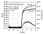
도 3은 산화물 반도체를 포함하는 절연 게이트 트랜지스터의 VG-ID 특성을 도시한 도면.
도 4a 및 도 4b는 산화물 반도체를 포함하는 절연 게이트 트랜지스터의 사진.
도 5a 및 도 5b는 산화물 반도체를 포함하는 절연 게이트 트랜지스터의 VG-ID 특성(온도 특성)을 도시한 도면.
도 6은 산화물 반도체를 포함하는 역 스태거형의 절연 게이트 트랜지스터의 종단면도.
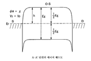
도 7a 및 도 7b는 도 6의 선 A-A'를 따라 절취한 단면에 대응하는 에너지 밴드도(모식도).
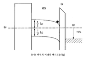
도 8a 및 도 8b는 도 6의 선 B-B'를 따라 절취한 단면에 대응하는 에너지 밴드도(모식도)로서, 도 8a는 양의 전위(VG>0)가 게이트(G1)에 공급된 상태를 도시하고 도 8b는 음의 전위(VG<0)가 게이트(G1)에 공급된 상태를 도시한다.
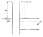
도 9는 진공 레벨, 금속의 일 함수(φM), 및 산화물 반도체의 전자 친화력(χ) 간의 관계를 도시한 도면.
도 10은 과학적 계산에 이용된 절연 게이트 트랜지스터의 구성 모델.
도 11a 내지 도 11d는 과학적 계산에 의해 임계 전압을 계산하여 얻어진 결과를 도시한 도면.
도 12a 및 도 12b는 전자 장치를 도시한 도면.
도 13a 및 도 13b는 전자 장치를 도시한 도면.
도 14a 및 도 14b는 전자 장치를 도시한 도면.
도 15는 본 발명의 실시 형태에 따른 트랜지스터를 도시한 단면도.
도 16은 본 발명의 실시 형태에 따른 트랜지스터의 VG-ID 특성을 도시한 도면.
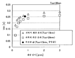
도 17은 본 발명의 실시 형태에 따른 트랜지스터의 임계 전압 및 과학적 계산 결과가 비교되는 그래프.


Claims (14)
- 반도체 장치로서,
게이트 전극층;
상기 게이트 전극층에 인접한 게이트 절연층; 및
상기 게이트 절연층을 사이에 두고 상기 게이트 전극층에 인접한 산화물 반도체층을 포함하고,
상기 산화물 반도체층은 인듐, 갈륨, 및 아연을 포함하고,
상기 산화물 반도체층은 결정을 포함하고,
상기 산화물 반도체층의 두께는 15nm 내지 30nm이고,
1V 내지 10V의 드레인 전압이 인가될 때, 채널 폭의 마이크로미터 당 오프 전류는 100aA/㎛ 이하이고,
상기 게이트 절연층의 두께는 20nm 내지 50nm인, 반도체 장치. - 반도체 장치로서,
게이트 전극층;
상기 게이트 전극층에 인접한 게이트 절연층; 및
상기 게이트 절연층을 사이에 두고 상기 게이트 전극층에 인접한 산화물 반도체층을 포함하고,
상기 산화물 반도체층은 인듐, 갈륨, 및 아연을 포함하고,
상기 산화물 반도체층은 결정을 포함하고,
상기 산화물 반도체층의 두께는 15nm 내지 100nm이고,
1V 내지 10V의 드레인 전압이 인가될 때, 채널 폭의 마이크로미터 당 오프 전류는 100aA/㎛ 이하이고,
상기 게이트 절연층의 두께는 10nm 내지 20nm인, 반도체 장치. - 제1항 또는 제2항에 있어서,
소스 전극층 및 드레인 전극층을 더 포함하고,
상기 소스 전극층 및 상기 드레인 전극층 각각은 상기 산화물 반도체층과 전기적으로 접속되는, 반도체 장치. - 반도체 장치로서,
산화물 반도체층;
상기 산화물 반도체층 위의 소스 전극층 및 드레인 전극층;
상기 산화물 반도체층, 상기 소스 전극층, 및 상기 드레인 전극층 위의 게이트 절연층; 및
상기 게이트 절연층 위의 게이트 전극층을 포함하고,
상기 게이트 전극층은 상기 산화물 반도체층, 상기 소스 전극층, 및 상기 드레인 전극층과 중첩하고,
상기 산화물 반도체층은 인듐, 갈륨, 및 아연을 포함하고,
상기 산화물 반도체층은 결정을 포함하고,
상기 산화물 반도체층의 두께는 15nm 내지 30nm이고,
1V 내지 10V의 드레인 전압이 인가될 때, 채널 폭의 마이크로미터 당 오프 전류는 100aA/㎛ 이하이고,
상기 게이트 절연층의 두께는 20nm 내지 50nm인, 반도체 장치. - 제4항에 있어서,
절연층을 더 포함하고,
상기 산화물 반도체층은 상기 절연층 위에 있는, 반도체 장치. - 제5항에 있어서,
도전층을 더 포함하고,
상기 절연층은 상기 도전층 위에 있는, 반도체 장치. - 제1항, 제2항, 및 제4항 중 어느 한 항에 있어서,
상기 산화물 반도체층의 캐리어 농도는 1×10¹²/cm3 미만인, 반도체 장치. - 제1항, 제2항, 및 제4항 중 어느 한 항에 있어서,
상기 게이트 전극층은 알루미늄, 구리, 몰리브덴, 티타늄, 크롬, 탄탈, 텅스텐, 네오디뮴, 및 스칸듐으로부터 선택된 금속 원소를 포함하는 막; 합금막; 또는 이들 중 임의의 것의 적층막을 포함하는, 반도체 장치. - 제1항, 제2항, 및 제4항 중 어느 한 항에 있어서,
상기 게이트 절연층은 산화 실리콘, 산화 질화 실리콘, 질화 산화 실리콘, 질화 실리콘, 산화 알루미늄, 산화 하프늄, 및 산화 탄탈 중 임의의 것의 단층막 또는 라미네이트막(laminate film)을 포함하는, 반도체 장치. - 제4항에 있어서,
상기 소스 전극층 및 상기 드레인 전극층 각각은 테이퍼 형상을 갖는, 반도체 장치. - 제1항, 제2항, 및 제4항 중 어느 한 항에 있어서,
상기 산화물 반도체층 내에 형성된 채널의 길이는 3.0㎛ 이하인, 반도체 장치. - 제11항에 있어서,
상기 산화물 반도체층 내에 형성된 채널의 길이는 0.2㎛ 이상인, 반도체 장치. - 제1항, 제2항, 및 제4항 중 어느 한 항에 있어서,
상기 결정의 지름은 1nm 이상이고, 20nm 이하인, 반도체 장치. - 전자 장치로서,
제1항, 제2항, 및 제4항 중 어느 한 항에 따른 반도체 장치를 포함하는, 전자 장치.
Applications Claiming Priority (3)
| Application Number | Priority Date | Filing Date | Title |
|---|---|---|---|
| JPJP-P-2009-270809 | 2009-11-27 | ||
| JP2009270809 | 2009-11-27 | ||
| PCT/JP2010/069648 WO2011065198A1 (en) | 2009-11-27 | 2010-10-28 | Semiconductor device |
Related Parent Applications (1)
| Application Number | Title | Priority Date | Filing Date |
|---|---|---|---|
| KR1020127013902A Division KR20120099450A (ko) | 2009-11-27 | 2010-10-28 | 반도체 장치 |
Related Child Applications (1)
| Application Number | Title | Priority Date | Filing Date |
|---|---|---|---|
| KR1020187014854A Division KR20180059577A (ko) | 2009-11-27 | 2010-10-28 | 반도체 장치 |
Publications (1)
| Publication Number | Publication Date |
|---|---|
| KR20170091760A true KR20170091760A (ko) | 2017-08-09 |
Family
ID=44066301
Family Applications (3)
| Application Number | Title | Priority Date | Filing Date |
|---|---|---|---|
| KR1020177021208A Ceased KR20170091760A (ko) | 2009-11-27 | 2010-10-28 | 반도체 장치 |
| KR1020127013902A Ceased KR20120099450A (ko) | 2009-11-27 | 2010-10-28 | 반도체 장치 |
| KR1020187014854A Ceased KR20180059577A (ko) | 2009-11-27 | 2010-10-28 | 반도체 장치 |
Family Applications After (2)
| Application Number | Title | Priority Date | Filing Date |
|---|---|---|---|
| KR1020127013902A Ceased KR20120099450A (ko) | 2009-11-27 | 2010-10-28 | 반도체 장치 |
| KR1020187014854A Ceased KR20180059577A (ko) | 2009-11-27 | 2010-10-28 | 반도체 장치 |
Country Status (6)
| Country | Link |
|---|---|
| US (4) | US8373203B2 (ko) |
| JP (4) | JP5701582B2 (ko) |
| KR (3) | KR20170091760A (ko) |
| CN (1) | CN102640293B (ko) |
| TW (3) | TWI632687B (ko) |
| WO (1) | WO2011065198A1 (ko) |
Families Citing this family (38)
| Publication number | Priority date | Publication date | Assignee | Title |
|---|---|---|---|---|
| KR20170091760A (ko) * | 2009-11-27 | 2017-08-09 | 가부시키가이샤 한도오따이 에네루기 켄큐쇼 | 반도체 장치 |
| US20120298998A1 (en) * | 2011-05-25 | 2012-11-29 | Semiconductor Energy Laboratory Co., Ltd. | Method for forming oxide semiconductor film, semiconductor device, and method for manufacturing semiconductor device |
| WO2013001579A1 (ja) * | 2011-06-30 | 2013-01-03 | パナソニック株式会社 | 薄膜トランジスタ装置及び薄膜トランジスタ装置の製造方法 |
| CN102969362B (zh) * | 2011-09-01 | 2016-03-30 | 中国科学院微电子研究所 | 高稳定性非晶态金属氧化物tft器件 |
| JP5825744B2 (ja) | 2011-09-15 | 2015-12-02 | 株式会社半導体エネルギー研究所 | パワー絶縁ゲート型電界効果トランジスタ |
| US8716708B2 (en) | 2011-09-29 | 2014-05-06 | Semiconductor Energy Laboratory Co., Ltd. | Semiconductor device and method for manufacturing the same |
| US8860023B2 (en) | 2012-05-01 | 2014-10-14 | Semiconductor Energy Laboratory Co., Ltd. | Semiconductor device |
| US20140027762A1 (en) * | 2012-07-27 | 2014-01-30 | Semiconductor Energy Laboratory Co. Ltd. | Semiconductor device |
| CN102789107A (zh) * | 2012-09-07 | 2012-11-21 | 深圳市华星光电技术有限公司 | 液晶显示面板 |
| WO2014042187A1 (ja) * | 2012-09-14 | 2014-03-20 | シャープ株式会社 | アクティブマトリクス基板、表示パネル及び表示装置 |
| WO2014054558A1 (ja) * | 2012-10-03 | 2014-04-10 | シャープ株式会社 | 半導体装置及び表示装置 |
| CN102856392B (zh) * | 2012-10-09 | 2015-12-02 | 深圳市华星光电技术有限公司 | 薄膜晶体管主动装置及其制作方法 |
| CN103048840B (zh) * | 2012-11-12 | 2015-04-01 | 京东方科技集团股份有限公司 | 阵列基板及其制作方法、液晶显示面板和显示装置 |
| KR102101863B1 (ko) * | 2013-01-07 | 2020-04-21 | 삼성디스플레이 주식회사 | 박막 트랜지스터, 이의 제조 방법 및 이를 구비하는 표시 장치 |
| JP2015032520A (ja) * | 2013-08-05 | 2015-02-16 | 株式会社神戸製鋼所 | 有機elディスプレイ |
| KR101512726B1 (ko) * | 2013-10-15 | 2015-04-20 | 연세대학교 산학협력단 | 패시베이션층 조성물, 패시베이션 방법, 박막 트랜지스터 및 박막 트랜지스터 제조 방법 |
| CN103700699A (zh) * | 2013-12-19 | 2014-04-02 | 深圳市华星光电技术有限公司 | 一种栅金属结构及其制造方法 |
| JP6227396B2 (ja) * | 2013-12-20 | 2017-11-08 | 株式会社ジャパンディスプレイ | 薄膜トランジスタ及びそれを用いた表示装置 |
| US20160155849A1 (en) * | 2014-12-02 | 2016-06-02 | Semiconductor Energy Laboratory Co., Ltd. | Semiconductor device, method for manufacturing semiconductor device, module, and electronic device |
| CN104992951A (zh) * | 2015-06-19 | 2015-10-21 | 深圳市华星光电技术有限公司 | 一种阵列基板及其制成方法、显示面板 |
| KR101788929B1 (ko) * | 2015-09-25 | 2017-11-15 | 아주대학교산학협력단 | 금속산화물 박막의 전기 전도도 향상 방법 및 이에 의해 전도도가 조절된 금속산화물 박막을 포함하는 박막트랜지스터 |
| CN108352358B (zh) | 2015-10-13 | 2022-07-26 | 非结晶公司 | 非晶金属薄膜非线性电阻器 |
| US9806179B2 (en) * | 2016-01-14 | 2017-10-31 | Hon Hai Precision Industry Co., Ltd. | Method for fabricating conducting structure and thin film transistor array panel |
| US10672898B2 (en) | 2016-07-07 | 2020-06-02 | Amorphyx, Incorporated | Amorphous metal hot electron transistor |
| KR101914835B1 (ko) * | 2016-11-18 | 2018-11-02 | 아주대학교산학협력단 | 금속산화물 이종 접합 구조, 이의 제조방법 및 이를 포함하는 박막트랜지스터 |
| CN107799608A (zh) * | 2017-11-13 | 2018-03-13 | 华南理工大学 | 一种薄膜晶体管及其制备方法和应用 |
| CN107978610B (zh) * | 2017-11-30 | 2020-04-24 | 上海天马微电子有限公司 | 一种阵列基板、显示面板、显示装置及阵列基板的制造方法 |
| JP2019161182A (ja) * | 2018-03-16 | 2019-09-19 | 株式会社リコー | 電界効果型トランジスタ及びその製造方法、表示素子、表示装置、システム |
| JP2021520060A (ja) | 2018-03-30 | 2021-08-12 | アモルフィックス・インコーポレイテッド | アモルファス金属薄膜トランジスタ |
| KR102737478B1 (ko) | 2018-12-07 | 2024-12-03 | 아모르픽스, 인크 | 다이오드 기반 디스플레이 백플레인 및 전자 디스플레이를 위한 방법 및 회로 |
| CN109638082B (zh) * | 2018-12-12 | 2021-05-25 | 华南理工大学 | 薄膜晶体管以及制备方法 |
| CN109638070B (zh) * | 2018-12-12 | 2021-01-15 | 广州新视界光电科技有限公司 | 氧化物半导体材料、薄膜晶体管及制备方法和显示面板 |
| KR102727034B1 (ko) * | 2019-09-03 | 2024-11-07 | 삼성디스플레이 주식회사 | 표시 장치 및 제조 방법 |
| US20220230878A1 (en) * | 2019-09-05 | 2022-07-21 | Hewlett-Packard Development Company, L.P. | Semiconductor composite layers |
| CN111129162B (zh) * | 2019-12-31 | 2022-10-04 | 华南理工大学 | 一种薄膜晶体管、显示基板、显示面板及显示装置 |
| KR102828158B1 (ko) * | 2020-01-14 | 2025-07-01 | 아주대학교산학협력단 | 금속산화물 이종접합 구조물 및 이를 포함하는 전자 소자 |
| CN113661574B (zh) * | 2020-03-12 | 2024-04-09 | 京东方科技集团股份有限公司 | 显示基板及其制备方法、显示面板 |
| JP7803887B2 (ja) | 2020-06-12 | 2026-01-21 | アモルフィックス・インコーポレイテッド | 電子デバイスのための非線形構成要素を含む回路 |
Family Cites Families (130)
| Publication number | Priority date | Publication date | Assignee | Title |
|---|---|---|---|---|
| JPS60198861A (ja) | 1984-03-23 | 1985-10-08 | Fujitsu Ltd | 薄膜トランジスタ |
| JPH0244256B2 (ja) | 1987-01-28 | 1990-10-03 | Kagaku Gijutsucho Mukizaishitsu Kenkyushocho | Ingazn2o5deshimesarerurotsuhoshokeinosojokozoojusurukagobutsuoyobisonoseizoho |
| JPH0244260B2 (ja) | 1987-02-24 | 1990-10-03 | Kagaku Gijutsucho Mukizaishitsu Kenkyushocho | Ingazn5o8deshimesarerurotsuhoshokeinosojokozoojusurukagobutsuoyobisonoseizoho |
| JPH0244258B2 (ja) | 1987-02-24 | 1990-10-03 | Kagaku Gijutsucho Mukizaishitsu Kenkyushocho | Ingazn3o6deshimesarerurotsuhoshokeinosojokozoojusurukagobutsuoyobisonoseizoho |
| JPS63210023A (ja) | 1987-02-24 | 1988-08-31 | Natl Inst For Res In Inorg Mater | InGaZn↓4O↓7で示される六方晶系の層状構造を有する化合物およびその製造法 |
| JPH0244262B2 (ja) | 1987-02-27 | 1990-10-03 | Kagaku Gijutsucho Mukizaishitsu Kenkyushocho | Ingazn6o9deshimesarerurotsuhoshokeinosojokozoojusurukagobutsuoyobisonoseizoho |
| JPH0244263B2 (ja) | 1987-04-22 | 1990-10-03 | Kagaku Gijutsucho Mukizaishitsu Kenkyushocho | Ingazn7o10deshimesarerurotsuhoshokeinosojokozoojusurukagobutsuoyobisonoseizoho |
| JPH05251705A (ja) | 1992-03-04 | 1993-09-28 | Fuji Xerox Co Ltd | 薄膜トランジスタ |
| JP3479375B2 (ja) | 1995-03-27 | 2003-12-15 | 科学技術振興事業団 | 亜酸化銅等の金属酸化物半導体による薄膜トランジスタとpn接合を形成した金属酸化物半導体装置およびそれらの製造方法 |
| WO1997006554A2 (en) * | 1995-08-03 | 1997-02-20 | Philips Electronics N.V. | Semiconductor device provided with transparent switching element |
| JP3625598B2 (ja) * | 1995-12-30 | 2005-03-02 | 三星電子株式会社 | 液晶表示装置の製造方法 |
| JP4170454B2 (ja) | 1998-07-24 | 2008-10-22 | Hoya株式会社 | 透明導電性酸化物薄膜を有する物品及びその製造方法 |
| JP2000150861A (ja) * | 1998-11-16 | 2000-05-30 | Tdk Corp | 酸化物薄膜 |
| JP3276930B2 (ja) * | 1998-11-17 | 2002-04-22 | 科学技術振興事業団 | トランジスタ及び半導体装置 |
| TW460731B (en) * | 1999-09-03 | 2001-10-21 | Ind Tech Res Inst | Electrode structure and production method of wide viewing angle LCD |
| JP4089858B2 (ja) | 2000-09-01 | 2008-05-28 | 国立大学法人東北大学 | 半導体デバイス |
| KR20020038482A (ko) * | 2000-11-15 | 2002-05-23 | 모리시타 요이찌 | 박막 트랜지스터 어레이, 그 제조방법 및 그것을 이용한표시패널 |
| JP2002222973A (ja) * | 2001-01-29 | 2002-08-09 | Sharp Corp | 光電変換素子およびその製造方法 |
| JP3997731B2 (ja) * | 2001-03-19 | 2007-10-24 | 富士ゼロックス株式会社 | 基材上に結晶性半導体薄膜を形成する方法 |
| JP2002289859A (ja) | 2001-03-23 | 2002-10-04 | Minolta Co Ltd | 薄膜トランジスタ |
| JP4439766B2 (ja) * | 2001-08-02 | 2010-03-24 | シャープ株式会社 | 薄膜トランジスタ装置及びその製造方法 |
| JP4090716B2 (ja) * | 2001-09-10 | 2008-05-28 | 雅司 川崎 | 薄膜トランジスタおよびマトリクス表示装置 |
| JP3925839B2 (ja) | 2001-09-10 | 2007-06-06 | シャープ株式会社 | 半導体記憶装置およびその試験方法 |
| US7061014B2 (en) * | 2001-11-05 | 2006-06-13 | Japan Science And Technology Agency | Natural-superlattice homologous single crystal thin film, method for preparation thereof, and device using said single crystal thin film |
| JP4164562B2 (ja) | 2002-09-11 | 2008-10-15 | 独立行政法人科学技術振興機構 | ホモロガス薄膜を活性層として用いる透明薄膜電界効果型トランジスタ |
| JP4083486B2 (ja) * | 2002-02-21 | 2008-04-30 | 独立行政法人科学技術振興機構 | LnCuO(S,Se,Te)単結晶薄膜の製造方法 |
| US7049190B2 (en) * | 2002-03-15 | 2006-05-23 | Sanyo Electric Co., Ltd. | Method for forming ZnO film, method for forming ZnO semiconductor layer, method for fabricating semiconductor device, and semiconductor device |
| JP3933591B2 (ja) * | 2002-03-26 | 2007-06-20 | 淳二 城戸 | 有機エレクトロルミネッセント素子 |
| US7339187B2 (en) * | 2002-05-21 | 2008-03-04 | State Of Oregon Acting By And Through The Oregon State Board Of Higher Education On Behalf Of Oregon State University | Transistor structures |
| JP2004022625A (ja) * | 2002-06-13 | 2004-01-22 | Murata Mfg Co Ltd | 半導体デバイス及び該半導体デバイスの製造方法 |
| US7105868B2 (en) * | 2002-06-24 | 2006-09-12 | Cermet, Inc. | High-electron mobility transistor with zinc oxide |
| US7067843B2 (en) * | 2002-10-11 | 2006-06-27 | E. I. Du Pont De Nemours And Company | Transparent oxide semiconductor thin film transistors |
| JP4166105B2 (ja) | 2003-03-06 | 2008-10-15 | シャープ株式会社 | 半導体装置およびその製造方法 |
| JP2004273732A (ja) | 2003-03-07 | 2004-09-30 | Sharp Corp | アクティブマトリクス基板およびその製造方法 |
| JP4108633B2 (ja) | 2003-06-20 | 2008-06-25 | シャープ株式会社 | 薄膜トランジスタおよびその製造方法ならびに電子デバイス |
| US7262463B2 (en) * | 2003-07-25 | 2007-08-28 | Hewlett-Packard Development Company, L.P. | Transistor including a deposited channel region having a doped portion |
| US7145174B2 (en) * | 2004-03-12 | 2006-12-05 | Hewlett-Packard Development Company, Lp. | Semiconductor device |
| KR20070116888A (ko) * | 2004-03-12 | 2007-12-11 | 도꾸리쯔교세이호징 가가꾸 기쥬쯔 신꼬 기꼬 | 아몰퍼스 산화물 및 박막 트랜지스터 |
| US7297977B2 (en) * | 2004-03-12 | 2007-11-20 | Hewlett-Packard Development Company, L.P. | Semiconductor device |
| US7282782B2 (en) * | 2004-03-12 | 2007-10-16 | Hewlett-Packard Development Company, L.P. | Combined binary oxide semiconductor device |
| US7211825B2 (en) * | 2004-06-14 | 2007-05-01 | Yi-Chi Shih | Indium oxide-based thin film transistors and circuits |
| JP2006100760A (ja) * | 2004-09-02 | 2006-04-13 | Casio Comput Co Ltd | 薄膜トランジスタおよびその製造方法 |
| US7285501B2 (en) * | 2004-09-17 | 2007-10-23 | Hewlett-Packard Development Company, L.P. | Method of forming a solution processed device |
| US7298084B2 (en) * | 2004-11-02 | 2007-11-20 | 3M Innovative Properties Company | Methods and displays utilizing integrated zinc oxide row and column drivers in conjunction with organic light emitting diodes |
| EP2453481B1 (en) * | 2004-11-10 | 2017-01-11 | Canon Kabushiki Kaisha | Field effect transistor with amorphous oxide |
| US7863611B2 (en) * | 2004-11-10 | 2011-01-04 | Canon Kabushiki Kaisha | Integrated circuits utilizing amorphous oxides |
| US7791072B2 (en) * | 2004-11-10 | 2010-09-07 | Canon Kabushiki Kaisha | Display |
| US7453065B2 (en) * | 2004-11-10 | 2008-11-18 | Canon Kabushiki Kaisha | Sensor and image pickup device |
| CA2585063C (en) * | 2004-11-10 | 2013-01-15 | Canon Kabushiki Kaisha | Light-emitting device |
| BRPI0517560B8 (pt) * | 2004-11-10 | 2018-12-11 | Canon Kk | transistor de efeito de campo |
| US7829444B2 (en) * | 2004-11-10 | 2010-11-09 | Canon Kabushiki Kaisha | Field effect transistor manufacturing method |
| KR20060064264A (ko) | 2004-12-08 | 2006-06-13 | 삼성전자주식회사 | 박막 트랜지스터 표시판 및 그 제조 방법 |
| US7579224B2 (en) * | 2005-01-21 | 2009-08-25 | Semiconductor Energy Laboratory Co., Ltd. | Method for manufacturing a thin film semiconductor device |
| TWI505473B (zh) * | 2005-01-28 | 2015-10-21 | 半導體能源研究所股份有限公司 | 半導體裝置,電子裝置,和半導體裝置的製造方法 |
| US7608531B2 (en) * | 2005-01-28 | 2009-10-27 | Semiconductor Energy Laboratory Co., Ltd. | Semiconductor device, electronic device, and method of manufacturing semiconductor device |
| US7858451B2 (en) * | 2005-02-03 | 2010-12-28 | Semiconductor Energy Laboratory Co., Ltd. | Electronic device, semiconductor device and manufacturing method thereof |
| US7948171B2 (en) * | 2005-02-18 | 2011-05-24 | Semiconductor Energy Laboratory Co., Ltd. | Light emitting device |
| JP4851103B2 (ja) * | 2005-03-01 | 2012-01-11 | 学校法人常翔学園 | 酸化亜鉛系トランジスタ |
| US20060197092A1 (en) * | 2005-03-03 | 2006-09-07 | Randy Hoffman | System and method for forming conductive material on a substrate |
| US8681077B2 (en) * | 2005-03-18 | 2014-03-25 | Semiconductor Energy Laboratory Co., Ltd. | Semiconductor device, and display device, driving method and electronic apparatus thereof |
| WO2006105077A2 (en) * | 2005-03-28 | 2006-10-05 | Massachusetts Institute Of Technology | Low voltage thin film transistor with high-k dielectric material |
| US7645478B2 (en) * | 2005-03-31 | 2010-01-12 | 3M Innovative Properties Company | Methods of making displays |
| US8300031B2 (en) * | 2005-04-20 | 2012-10-30 | Semiconductor Energy Laboratory Co., Ltd. | Semiconductor device comprising transistor having gate and drain connected through a current-voltage conversion element |
| JP5127161B2 (ja) * | 2005-05-30 | 2013-01-23 | 株式会社半導体エネルギー研究所 | 半導体装置 |
| JP2006344849A (ja) * | 2005-06-10 | 2006-12-21 | Casio Comput Co Ltd | 薄膜トランジスタ |
| US7402506B2 (en) * | 2005-06-16 | 2008-07-22 | Eastman Kodak Company | Methods of making thin film transistors comprising zinc-oxide-based semiconductor materials and transistors made thereby |
| US7691666B2 (en) * | 2005-06-16 | 2010-04-06 | Eastman Kodak Company | Methods of making thin film transistors comprising zinc-oxide-based semiconductor materials and transistors made thereby |
| US7507618B2 (en) * | 2005-06-27 | 2009-03-24 | 3M Innovative Properties Company | Method for making electronic devices using metal oxide nanoparticles |
| JP2007035867A (ja) | 2005-07-26 | 2007-02-08 | Oki Electric Ind Co Ltd | 半導体装置 |
| KR100711890B1 (ko) * | 2005-07-28 | 2007-04-25 | 삼성에스디아이 주식회사 | 유기 발광표시장치 및 그의 제조방법 |
| JP2007059128A (ja) * | 2005-08-23 | 2007-03-08 | Canon Inc | 有機el表示装置およびその製造方法 |
| JP2007073705A (ja) * | 2005-09-06 | 2007-03-22 | Canon Inc | 酸化物半導体チャネル薄膜トランジスタおよびその製造方法 |
| JP4280736B2 (ja) * | 2005-09-06 | 2009-06-17 | キヤノン株式会社 | 半導体素子 |
| JP4850457B2 (ja) * | 2005-09-06 | 2012-01-11 | キヤノン株式会社 | 薄膜トランジスタ及び薄膜ダイオード |
| JP4560502B2 (ja) | 2005-09-06 | 2010-10-13 | キヤノン株式会社 | 電界効果型トランジスタ |
| JP5116225B2 (ja) * | 2005-09-06 | 2013-01-09 | キヤノン株式会社 | 酸化物半導体デバイスの製造方法 |
| JP5078246B2 (ja) | 2005-09-29 | 2012-11-21 | 株式会社半導体エネルギー研究所 | 半導体装置、及び半導体装置の作製方法 |
| JP5064747B2 (ja) | 2005-09-29 | 2012-10-31 | 株式会社半導体エネルギー研究所 | 半導体装置、電気泳動表示装置、表示モジュール、電子機器、及び半導体装置の作製方法 |
| EP3614442A3 (en) * | 2005-09-29 | 2020-03-25 | Semiconductor Energy Laboratory Co., Ltd. | Semiconductor device having oxide semiconductor layer and manufactoring method thereof |
| JP5037808B2 (ja) * | 2005-10-20 | 2012-10-03 | キヤノン株式会社 | アモルファス酸化物を用いた電界効果型トランジスタ、及び該トランジスタを用いた表示装置 |
| KR20090115222A (ko) | 2005-11-15 | 2009-11-04 | 가부시키가이샤 한도오따이 에네루기 켄큐쇼 | 반도체장치 제조방법 |
| JP5089139B2 (ja) * | 2005-11-15 | 2012-12-05 | 株式会社半導体エネルギー研究所 | 半導体装置の作製方法 |
| TWI292281B (en) * | 2005-12-29 | 2008-01-01 | Ind Tech Res Inst | Pixel structure of active organic light emitting diode and method of fabricating the same |
| US7867636B2 (en) * | 2006-01-11 | 2011-01-11 | Murata Manufacturing Co., Ltd. | Transparent conductive film and method for manufacturing the same |
| JP4977478B2 (ja) * | 2006-01-21 | 2012-07-18 | 三星電子株式会社 | ZnOフィルム及びこれを用いたTFTの製造方法 |
| US7576394B2 (en) * | 2006-02-02 | 2009-08-18 | Kochi Industrial Promotion Center | Thin film transistor including low resistance conductive thin films and manufacturing method thereof |
| US7977169B2 (en) * | 2006-02-15 | 2011-07-12 | Kochi Industrial Promotion Center | Semiconductor device including active layer made of zinc oxide with controlled orientations and manufacturing method thereof |
| JP5015471B2 (ja) * | 2006-02-15 | 2012-08-29 | 財団法人高知県産業振興センター | 薄膜トランジスタ及びその製法 |
| KR20070101595A (ko) * | 2006-04-11 | 2007-10-17 | 삼성전자주식회사 | ZnO TFT |
| US20070252928A1 (en) * | 2006-04-28 | 2007-11-01 | Toppan Printing Co., Ltd. | Structure, transmission type liquid crystal display, reflection type display and manufacturing method thereof |
| JP5028033B2 (ja) * | 2006-06-13 | 2012-09-19 | キヤノン株式会社 | 酸化物半導体膜のドライエッチング方法 |
| JP4999400B2 (ja) * | 2006-08-09 | 2012-08-15 | キヤノン株式会社 | 酸化物半導体膜のドライエッチング方法 |
| JP4609797B2 (ja) * | 2006-08-09 | 2011-01-12 | Nec液晶テクノロジー株式会社 | 薄膜デバイス及びその製造方法 |
| JP4332545B2 (ja) * | 2006-09-15 | 2009-09-16 | キヤノン株式会社 | 電界効果型トランジスタ及びその製造方法 |
| JP4274219B2 (ja) * | 2006-09-27 | 2009-06-03 | セイコーエプソン株式会社 | 電子デバイス、有機エレクトロルミネッセンス装置、有機薄膜半導体装置 |
| JP5164357B2 (ja) * | 2006-09-27 | 2013-03-21 | キヤノン株式会社 | 半導体装置及び半導体装置の製造方法 |
| US7622371B2 (en) * | 2006-10-10 | 2009-11-24 | Hewlett-Packard Development Company, L.P. | Fused nanocrystal thin film semiconductor and method |
| US7772021B2 (en) * | 2006-11-29 | 2010-08-10 | Samsung Electronics Co., Ltd. | Flat panel displays comprising a thin-film transistor having a semiconductive oxide in its channel and methods of fabricating the same for use in flat panel displays |
| JP2008140684A (ja) * | 2006-12-04 | 2008-06-19 | Toppan Printing Co Ltd | カラーelディスプレイおよびその製造方法 |
| WO2008069255A1 (en) | 2006-12-05 | 2008-06-12 | Canon Kabushiki Kaisha | Method for manufacturing thin film transistor using oxide semiconductor and display apparatus |
| JP5500771B2 (ja) * | 2006-12-05 | 2014-05-21 | 株式会社半導体エネルギー研究所 | 半導体装置及びマイクロプロセッサ |
| US8143115B2 (en) | 2006-12-05 | 2012-03-27 | Canon Kabushiki Kaisha | Method for manufacturing thin film transistor using oxide semiconductor and display apparatus |
| JP5305630B2 (ja) | 2006-12-05 | 2013-10-02 | キヤノン株式会社 | ボトムゲート型薄膜トランジスタの製造方法及び表示装置の製造方法 |
| KR101303578B1 (ko) * | 2007-01-05 | 2013-09-09 | 삼성전자주식회사 | 박막 식각 방법 |
| US8207063B2 (en) * | 2007-01-26 | 2012-06-26 | Eastman Kodak Company | Process for atomic layer deposition |
| TWI478347B (zh) * | 2007-02-09 | 2015-03-21 | 出光興產股份有限公司 | A thin film transistor, a thin film transistor substrate, and an image display device, and an image display device, and a semiconductor device |
| KR100851215B1 (ko) * | 2007-03-14 | 2008-08-07 | 삼성에스디아이 주식회사 | 박막 트랜지스터 및 이를 이용한 유기 전계 발광표시장치 |
| JP5466939B2 (ja) * | 2007-03-23 | 2014-04-09 | 出光興産株式会社 | 半導体デバイス、多結晶半導体薄膜、多結晶半導体薄膜の製造方法、電界効果型トランジスタ、及び、電界効果型トランジスタの製造方法 |
| JP4727684B2 (ja) | 2007-03-27 | 2011-07-20 | 富士フイルム株式会社 | 薄膜電界効果型トランジスタおよびそれを用いた表示装置 |
| WO2008126879A1 (en) | 2007-04-09 | 2008-10-23 | Canon Kabushiki Kaisha | Light-emitting apparatus and production method thereof |
| JP5197058B2 (ja) | 2007-04-09 | 2013-05-15 | キヤノン株式会社 | 発光装置とその作製方法 |
| US7795613B2 (en) * | 2007-04-17 | 2010-09-14 | Toppan Printing Co., Ltd. | Structure with transistor |
| KR101325053B1 (ko) * | 2007-04-18 | 2013-11-05 | 삼성디스플레이 주식회사 | 박막 트랜지스터 기판 및 이의 제조 방법 |
| KR20080094300A (ko) * | 2007-04-19 | 2008-10-23 | 삼성전자주식회사 | 박막 트랜지스터 및 그 제조 방법과 박막 트랜지스터를포함하는 평판 디스플레이 |
| KR101334181B1 (ko) * | 2007-04-20 | 2013-11-28 | 삼성전자주식회사 | 선택적으로 결정화된 채널층을 갖는 박막 트랜지스터 및 그제조 방법 |
| CN101663762B (zh) * | 2007-04-25 | 2011-09-21 | 佳能株式会社 | 氧氮化物半导体 |
| US8748879B2 (en) | 2007-05-08 | 2014-06-10 | Idemitsu Kosan Co., Ltd. | Semiconductor device, thin film transistor and a method for producing the same |
| US7851352B2 (en) | 2007-05-11 | 2010-12-14 | Semiconductor Energy Laboratory Co., Ltd | Manufacturing method of semiconductor device and electronic device |
| KR101334182B1 (ko) * | 2007-05-28 | 2013-11-28 | 삼성전자주식회사 | ZnO 계 박막 트랜지스터의 제조방법 |
| KR101345376B1 (ko) * | 2007-05-29 | 2013-12-24 | 삼성전자주식회사 | ZnO 계 박막 트랜지스터 및 그 제조방법 |
| JP5430846B2 (ja) * | 2007-12-03 | 2014-03-05 | 株式会社半導体エネルギー研究所 | 半導体装置の作製方法 |
| JP5215158B2 (ja) * | 2007-12-17 | 2013-06-19 | 富士フイルム株式会社 | 無機結晶性配向膜及びその製造方法、半導体デバイス |
| JP2009260315A (ja) * | 2008-03-26 | 2009-11-05 | Semiconductor Energy Lab Co Ltd | Soi基板の作製方法及び半導体装置の作製方法 |
| JP5704790B2 (ja) * | 2008-05-07 | 2015-04-22 | キヤノン株式会社 | 薄膜トランジスタ、および、表示装置 |
| JP5305730B2 (ja) * | 2008-05-12 | 2013-10-02 | キヤノン株式会社 | 半導体素子の製造方法ならびにその製造装置 |
| JP5403390B2 (ja) * | 2008-05-16 | 2014-01-29 | 出光興産株式会社 | インジウム、ガリウム及び亜鉛を含む酸化物 |
| JP4623179B2 (ja) * | 2008-09-18 | 2011-02-02 | ソニー株式会社 | 薄膜トランジスタおよびその製造方法 |
| JP5451280B2 (ja) * | 2008-10-09 | 2014-03-26 | キヤノン株式会社 | ウルツ鉱型結晶成長用基板およびその製造方法ならびに半導体装置 |
| KR101772639B1 (ko) | 2009-10-16 | 2017-08-29 | 가부시키가이샤 한도오따이 에네루기 켄큐쇼 | 반도체 장치 |
| KR20170091760A (ko) * | 2009-11-27 | 2017-08-09 | 가부시키가이샤 한도오따이 에네루기 켄큐쇼 | 반도체 장치 |
-
2010
- 2010-10-28 KR KR1020177021208A patent/KR20170091760A/ko not_active Ceased
- 2010-10-28 KR KR1020127013902A patent/KR20120099450A/ko not_active Ceased
- 2010-10-28 WO PCT/JP2010/069648 patent/WO2011065198A1/en not_active Ceased
- 2010-10-28 CN CN201080053607.6A patent/CN102640293B/zh active Active
- 2010-10-28 KR KR1020187014854A patent/KR20180059577A/ko not_active Ceased
- 2010-11-22 TW TW106107978A patent/TWI632687B/zh active
- 2010-11-22 TW TW104135604A patent/TWI585981B/zh not_active IP Right Cessation
- 2010-11-22 TW TW099140219A patent/TWI517386B/zh active
- 2010-11-24 US US12/954,222 patent/US8373203B2/en active Active
- 2010-11-25 JP JP2010262011A patent/JP5701582B2/ja active Active
-
2013
- 2013-01-30 US US13/753,582 patent/US8680521B2/en active Active
-
2014
- 2014-03-13 US US14/207,750 patent/US9184299B2/en active Active
-
2015
- 2015-02-10 JP JP2015024126A patent/JP2015122530A/ja not_active Withdrawn
- 2015-11-06 US US14/934,387 patent/US9570628B2/en active Active
-
2017
- 2017-05-15 JP JP2017096151A patent/JP6349440B2/ja active Active
-
2018
- 2018-06-04 JP JP2018106804A patent/JP2018148232A/ja not_active Withdrawn
Also Published As
| Publication number | Publication date |
|---|---|
| US20140191232A1 (en) | 2014-07-10 |
| JP5701582B2 (ja) | 2015-04-15 |
| US8680521B2 (en) | 2014-03-25 |
| TW201138108A (en) | 2011-11-01 |
| JP2018148232A (ja) | 2018-09-20 |
| JP2011135059A (ja) | 2011-07-07 |
| TW201605052A (zh) | 2016-02-01 |
| TWI517386B (zh) | 2016-01-11 |
| JP2015122530A (ja) | 2015-07-02 |
| US20110127525A1 (en) | 2011-06-02 |
| KR20180059577A (ko) | 2018-06-04 |
| US9570628B2 (en) | 2017-02-14 |
| CN102640293A (zh) | 2012-08-15 |
| TWI632687B (zh) | 2018-08-11 |
| US20130140560A1 (en) | 2013-06-06 |
| US9184299B2 (en) | 2015-11-10 |
| CN102640293B (zh) | 2015-07-22 |
| KR20120099450A (ko) | 2012-09-10 |
| US8373203B2 (en) | 2013-02-12 |
| TW201727914A (zh) | 2017-08-01 |
| WO2011065198A1 (en) | 2011-06-03 |
| JP6349440B2 (ja) | 2018-06-27 |
| JP2017175152A (ja) | 2017-09-28 |
| US20160064572A1 (en) | 2016-03-03 |
| TWI585981B (zh) | 2017-06-01 |
Similar Documents
| Publication | Publication Date | Title |
|---|---|---|
| TWI517386B (zh) | 半導體裝置 | |
| US20260006918A1 (en) | Liquid crystal display device and electronic device | |
| JP6050020B2 (ja) | 酸化物半導体膜、及び半導体装置 | |
| JP5816330B2 (ja) | 半導体装置 | |
| US9123573B2 (en) | Oxide semiconductor stacked film and semiconductor device | |
| JP5707046B2 (ja) | 半導体装置の作製方法 | |
| KR102513073B1 (ko) | 반도체 장치 및 그 제작 방법 | |
| US9876099B2 (en) | Semiconductor device, display device, input/output device, and electronic device | |
| US10134781B2 (en) | Capacitor and semiconductor device | |
| US20160343870A1 (en) | Semiconductor device and method for manufacturing semiconductor device | |
| US9305774B2 (en) | Method for processing thin film and method for manufacturing semiconductor device | |
| US9716182B2 (en) | Semiconductor device | |
| JP6298353B2 (ja) | 半導体装置 |
Legal Events
| Date | Code | Title | Description |
|---|---|---|---|
| A107 | Divisional application of patent | ||
| A201 | Request for examination | ||
| PA0104 | Divisional application for international application |
Comment text: Divisional Application for International Patent Patent event code: PA01041R01D Patent event date: 20170727 Application number text: 1020127013902 Filing date: 20120529 |
|
| PA0201 | Request for examination | ||
| PG1501 | Laying open of application | ||
| E902 | Notification of reason for refusal | ||
| PE0902 | Notice of grounds for rejection |
Comment text: Notification of reason for refusal Patent event date: 20170929 Patent event code: PE09021S01D |
|
| E601 | Decision to refuse application | ||
| PE0601 | Decision on rejection of patent |
Patent event date: 20180425 Comment text: Decision to Refuse Application Patent event code: PE06012S01D Patent event date: 20170929 Comment text: Notification of reason for refusal Patent event code: PE06011S01I |
|
| A107 | Divisional application of patent | ||
| PA0104 | Divisional application for international application |
Comment text: Divisional Application for International Patent Patent event code: PA01041R01D Patent event date: 20180525 Application number text: 1020127013902 Filing date: 20120529 |