KR20170118210A - 기판 처리 시스템 및 기판 처리 방법, 그리고 디바이스 제조 방법 - Google Patents
기판 처리 시스템 및 기판 처리 방법, 그리고 디바이스 제조 방법 Download PDFInfo
- Publication number
- KR20170118210A KR20170118210A KR1020177026406A KR20177026406A KR20170118210A KR 20170118210 A KR20170118210 A KR 20170118210A KR 1020177026406 A KR1020177026406 A KR 1020177026406A KR 20177026406 A KR20177026406 A KR 20177026406A KR 20170118210 A KR20170118210 A KR 20170118210A
- Authority
- KR
- South Korea
- Prior art keywords
- substrate
- wafer
- measurement
- measuring
- marks
- Prior art date
- Legal status (The legal status is an assumption and is not a legal conclusion. Google has not performed a legal analysis and makes no representation as to the accuracy of the status listed.)
- Granted
Links
Images






Classifications
-
- G—PHYSICS
- G03—PHOTOGRAPHY; CINEMATOGRAPHY; ANALOGOUS TECHNIQUES USING WAVES OTHER THAN OPTICAL WAVES; ELECTROGRAPHY; HOLOGRAPHY
- G03F—PHOTOMECHANICAL PRODUCTION OF TEXTURED OR PATTERNED SURFACES, e.g. FOR PRINTING, FOR PROCESSING OF SEMICONDUCTOR DEVICES; MATERIALS THEREFOR; ORIGINALS THEREFOR; APPARATUS SPECIALLY ADAPTED THEREFOR
- G03F7/00—Photomechanical, e.g. photolithographic, production of textured or patterned surfaces, e.g. printing surfaces; Materials therefor, e.g. comprising photoresists; Apparatus specially adapted therefor
- G03F7/70—Microphotolithographic exposure; Apparatus therefor
- G03F7/70691—Handling of masks or workpieces
- G03F7/70775—Position control, e.g. interferometers or encoders for determining the stage position
-
- G—PHYSICS
- G03—PHOTOGRAPHY; CINEMATOGRAPHY; ANALOGOUS TECHNIQUES USING WAVES OTHER THAN OPTICAL WAVES; ELECTROGRAPHY; HOLOGRAPHY
- G03F—PHOTOMECHANICAL PRODUCTION OF TEXTURED OR PATTERNED SURFACES, e.g. FOR PRINTING, FOR PROCESSING OF SEMICONDUCTOR DEVICES; MATERIALS THEREFOR; ORIGINALS THEREFOR; APPARATUS SPECIALLY ADAPTED THEREFOR
- G03F9/00—Registration or positioning of originals, masks, frames, photographic sheets or textured or patterned surfaces, e.g. automatically
- G03F9/70—Registration or positioning of originals, masks, frames, photographic sheets or textured or patterned surfaces, e.g. automatically for microlithography
- G03F9/7003—Alignment type or strategy, e.g. leveling, global alignment
- G03F9/7046—Strategy, e.g. mark, sensor or wavelength selection
-
- G—PHYSICS
- G01—MEASURING; TESTING
- G01B—MEASURING LENGTH, THICKNESS OR SIMILAR LINEAR DIMENSIONS; MEASURING ANGLES; MEASURING AREAS; MEASURING IRREGULARITIES OF SURFACES OR CONTOURS
- G01B11/00—Measuring arrangements characterised by the use of optical techniques
-
- G—PHYSICS
- G01—MEASURING; TESTING
- G01B—MEASURING LENGTH, THICKNESS OR SIMILAR LINEAR DIMENSIONS; MEASURING ANGLES; MEASURING AREAS; MEASURING IRREGULARITIES OF SURFACES OR CONTOURS
- G01B11/00—Measuring arrangements characterised by the use of optical techniques
- G01B11/14—Measuring arrangements characterised by the use of optical techniques for measuring distance or clearance between spaced objects or spaced apertures
-
- G—PHYSICS
- G03—PHOTOGRAPHY; CINEMATOGRAPHY; ANALOGOUS TECHNIQUES USING WAVES OTHER THAN OPTICAL WAVES; ELECTROGRAPHY; HOLOGRAPHY
- G03F—PHOTOMECHANICAL PRODUCTION OF TEXTURED OR PATTERNED SURFACES, e.g. FOR PRINTING, FOR PROCESSING OF SEMICONDUCTOR DEVICES; MATERIALS THEREFOR; ORIGINALS THEREFOR; APPARATUS SPECIALLY ADAPTED THEREFOR
- G03F7/00—Photomechanical, e.g. photolithographic, production of textured or patterned surfaces, e.g. printing surfaces; Materials therefor, e.g. comprising photoresists; Apparatus specially adapted therefor
- G03F7/70—Microphotolithographic exposure; Apparatus therefor
- G03F7/70483—Information management; Active and passive control; Testing; Wafer monitoring, e.g. pattern monitoring
-
- G—PHYSICS
- G03—PHOTOGRAPHY; CINEMATOGRAPHY; ANALOGOUS TECHNIQUES USING WAVES OTHER THAN OPTICAL WAVES; ELECTROGRAPHY; HOLOGRAPHY
- G03F—PHOTOMECHANICAL PRODUCTION OF TEXTURED OR PATTERNED SURFACES, e.g. FOR PRINTING, FOR PROCESSING OF SEMICONDUCTOR DEVICES; MATERIALS THEREFOR; ORIGINALS THEREFOR; APPARATUS SPECIALLY ADAPTED THEREFOR
- G03F7/00—Photomechanical, e.g. photolithographic, production of textured or patterned surfaces, e.g. printing surfaces; Materials therefor, e.g. comprising photoresists; Apparatus specially adapted therefor
- G03F7/70—Microphotolithographic exposure; Apparatus therefor
- G03F7/70483—Information management; Active and passive control; Testing; Wafer monitoring, e.g. pattern monitoring
- G03F7/70491—Information management, e.g. software; Active and passive control, e.g. details of controlling exposure processes or exposure tool monitoring processes
- G03F7/705—Modelling or simulating from physical phenomena up to complete wafer processes or whole workflow in wafer productions
-
- G—PHYSICS
- G03—PHOTOGRAPHY; CINEMATOGRAPHY; ANALOGOUS TECHNIQUES USING WAVES OTHER THAN OPTICAL WAVES; ELECTROGRAPHY; HOLOGRAPHY
- G03F—PHOTOMECHANICAL PRODUCTION OF TEXTURED OR PATTERNED SURFACES, e.g. FOR PRINTING, FOR PROCESSING OF SEMICONDUCTOR DEVICES; MATERIALS THEREFOR; ORIGINALS THEREFOR; APPARATUS SPECIALLY ADAPTED THEREFOR
- G03F7/00—Photomechanical, e.g. photolithographic, production of textured or patterned surfaces, e.g. printing surfaces; Materials therefor, e.g. comprising photoresists; Apparatus specially adapted therefor
- G03F7/70—Microphotolithographic exposure; Apparatus therefor
- G03F7/70691—Handling of masks or workpieces
- G03F7/70716—Stages
-
- G—PHYSICS
- G03—PHOTOGRAPHY; CINEMATOGRAPHY; ANALOGOUS TECHNIQUES USING WAVES OTHER THAN OPTICAL WAVES; ELECTROGRAPHY; HOLOGRAPHY
- G03F—PHOTOMECHANICAL PRODUCTION OF TEXTURED OR PATTERNED SURFACES, e.g. FOR PRINTING, FOR PROCESSING OF SEMICONDUCTOR DEVICES; MATERIALS THEREFOR; ORIGINALS THEREFOR; APPARATUS SPECIALLY ADAPTED THEREFOR
- G03F7/00—Photomechanical, e.g. photolithographic, production of textured or patterned surfaces, e.g. printing surfaces; Materials therefor, e.g. comprising photoresists; Apparatus specially adapted therefor
- G03F7/70—Microphotolithographic exposure; Apparatus therefor
- G03F7/70691—Handling of masks or workpieces
- G03F7/70733—Handling masks and workpieces, e.g. exchange of workpiece or mask, transport of workpiece or mask
-
- G—PHYSICS
- G03—PHOTOGRAPHY; CINEMATOGRAPHY; ANALOGOUS TECHNIQUES USING WAVES OTHER THAN OPTICAL WAVES; ELECTROGRAPHY; HOLOGRAPHY
- G03F—PHOTOMECHANICAL PRODUCTION OF TEXTURED OR PATTERNED SURFACES, e.g. FOR PRINTING, FOR PROCESSING OF SEMICONDUCTOR DEVICES; MATERIALS THEREFOR; ORIGINALS THEREFOR; APPARATUS SPECIALLY ADAPTED THEREFOR
- G03F7/00—Photomechanical, e.g. photolithographic, production of textured or patterned surfaces, e.g. printing surfaces; Materials therefor, e.g. comprising photoresists; Apparatus specially adapted therefor
- G03F7/70—Microphotolithographic exposure; Apparatus therefor
- G03F7/70691—Handling of masks or workpieces
- G03F7/70783—Handling stress or warp of chucks, masks or workpieces, e.g. to compensate for imaging errors or considerations related to warpage of masks or workpieces due to their own weight
-
- G—PHYSICS
- G03—PHOTOGRAPHY; CINEMATOGRAPHY; ANALOGOUS TECHNIQUES USING WAVES OTHER THAN OPTICAL WAVES; ELECTROGRAPHY; HOLOGRAPHY
- G03F—PHOTOMECHANICAL PRODUCTION OF TEXTURED OR PATTERNED SURFACES, e.g. FOR PRINTING, FOR PROCESSING OF SEMICONDUCTOR DEVICES; MATERIALS THEREFOR; ORIGINALS THEREFOR; APPARATUS SPECIALLY ADAPTED THEREFOR
- G03F7/00—Photomechanical, e.g. photolithographic, production of textured or patterned surfaces, e.g. printing surfaces; Materials therefor, e.g. comprising photoresists; Apparatus specially adapted therefor
- G03F7/70—Microphotolithographic exposure; Apparatus therefor
- G03F7/708—Construction of apparatus, e.g. environment aspects, hygiene aspects or materials
- G03F7/7085—Detection arrangement, e.g. detectors of apparatus alignment possibly mounted on wafers, exposure dose, photo-cleaning flux, stray light, thermal load
-
- G—PHYSICS
- G03—PHOTOGRAPHY; CINEMATOGRAPHY; ANALOGOUS TECHNIQUES USING WAVES OTHER THAN OPTICAL WAVES; ELECTROGRAPHY; HOLOGRAPHY
- G03F—PHOTOMECHANICAL PRODUCTION OF TEXTURED OR PATTERNED SURFACES, e.g. FOR PRINTING, FOR PROCESSING OF SEMICONDUCTOR DEVICES; MATERIALS THEREFOR; ORIGINALS THEREFOR; APPARATUS SPECIALLY ADAPTED THEREFOR
- G03F7/00—Photomechanical, e.g. photolithographic, production of textured or patterned surfaces, e.g. printing surfaces; Materials therefor, e.g. comprising photoresists; Apparatus specially adapted therefor
- G03F7/70—Microphotolithographic exposure; Apparatus therefor
- G03F7/708—Construction of apparatus, e.g. environment aspects, hygiene aspects or materials
- G03F7/70858—Environment aspects, e.g. pressure of beam-path gas, temperature
- G03F7/70866—Environment aspects, e.g. pressure of beam-path gas, temperature of mask or workpiece
- G03F7/70875—Temperature, e.g. temperature control of masks or workpieces via control of stage temperature
-
- G—PHYSICS
- G03—PHOTOGRAPHY; CINEMATOGRAPHY; ANALOGOUS TECHNIQUES USING WAVES OTHER THAN OPTICAL WAVES; ELECTROGRAPHY; HOLOGRAPHY
- G03F—PHOTOMECHANICAL PRODUCTION OF TEXTURED OR PATTERNED SURFACES, e.g. FOR PRINTING, FOR PROCESSING OF SEMICONDUCTOR DEVICES; MATERIALS THEREFOR; ORIGINALS THEREFOR; APPARATUS SPECIALLY ADAPTED THEREFOR
- G03F7/00—Photomechanical, e.g. photolithographic, production of textured or patterned surfaces, e.g. printing surfaces; Materials therefor, e.g. comprising photoresists; Apparatus specially adapted therefor
- G03F7/70—Microphotolithographic exposure; Apparatus therefor
- G03F7/708—Construction of apparatus, e.g. environment aspects, hygiene aspects or materials
- G03F7/70991—Connection with other apparatus, e.g. multiple exposure stations, particular arrangement of exposure apparatus and pre-exposure and/or post-exposure apparatus; Shared apparatus, e.g. having shared radiation source, shared mask or workpiece stage, shared base-plate; Utilities, e.g. cable, pipe or wireless arrangements for data, power, fluids or vacuum
-
- G—PHYSICS
- G03—PHOTOGRAPHY; CINEMATOGRAPHY; ANALOGOUS TECHNIQUES USING WAVES OTHER THAN OPTICAL WAVES; ELECTROGRAPHY; HOLOGRAPHY
- G03F—PHOTOMECHANICAL PRODUCTION OF TEXTURED OR PATTERNED SURFACES, e.g. FOR PRINTING, FOR PROCESSING OF SEMICONDUCTOR DEVICES; MATERIALS THEREFOR; ORIGINALS THEREFOR; APPARATUS SPECIALLY ADAPTED THEREFOR
- G03F9/00—Registration or positioning of originals, masks, frames, photographic sheets or textured or patterned surfaces, e.g. automatically
- G03F9/70—Registration or positioning of originals, masks, frames, photographic sheets or textured or patterned surfaces, e.g. automatically for microlithography
- G03F9/7003—Alignment type or strategy, e.g. leveling, global alignment
-
- G—PHYSICS
- G03—PHOTOGRAPHY; CINEMATOGRAPHY; ANALOGOUS TECHNIQUES USING WAVES OTHER THAN OPTICAL WAVES; ELECTROGRAPHY; HOLOGRAPHY
- G03F—PHOTOMECHANICAL PRODUCTION OF TEXTURED OR PATTERNED SURFACES, e.g. FOR PRINTING, FOR PROCESSING OF SEMICONDUCTOR DEVICES; MATERIALS THEREFOR; ORIGINALS THEREFOR; APPARATUS SPECIALLY ADAPTED THEREFOR
- G03F9/00—Registration or positioning of originals, masks, frames, photographic sheets or textured or patterned surfaces, e.g. automatically
- G03F9/70—Registration or positioning of originals, masks, frames, photographic sheets or textured or patterned surfaces, e.g. automatically for microlithography
- G03F9/7003—Alignment type or strategy, e.g. leveling, global alignment
- G03F9/7023—Aligning or positioning in direction perpendicular to substrate surface
- G03F9/7034—Leveling
-
- G—PHYSICS
- G03—PHOTOGRAPHY; CINEMATOGRAPHY; ANALOGOUS TECHNIQUES USING WAVES OTHER THAN OPTICAL WAVES; ELECTROGRAPHY; HOLOGRAPHY
- G03F—PHOTOMECHANICAL PRODUCTION OF TEXTURED OR PATTERNED SURFACES, e.g. FOR PRINTING, FOR PROCESSING OF SEMICONDUCTOR DEVICES; MATERIALS THEREFOR; ORIGINALS THEREFOR; APPARATUS SPECIALLY ADAPTED THEREFOR
- G03F9/00—Registration or positioning of originals, masks, frames, photographic sheets or textured or patterned surfaces, e.g. automatically
- G03F9/70—Registration or positioning of originals, masks, frames, photographic sheets or textured or patterned surfaces, e.g. automatically for microlithography
- G03F9/7073—Alignment marks and their environment
-
- G—PHYSICS
- G03—PHOTOGRAPHY; CINEMATOGRAPHY; ANALOGOUS TECHNIQUES USING WAVES OTHER THAN OPTICAL WAVES; ELECTROGRAPHY; HOLOGRAPHY
- G03F—PHOTOMECHANICAL PRODUCTION OF TEXTURED OR PATTERNED SURFACES, e.g. FOR PRINTING, FOR PROCESSING OF SEMICONDUCTOR DEVICES; MATERIALS THEREFOR; ORIGINALS THEREFOR; APPARATUS SPECIALLY ADAPTED THEREFOR
- G03F9/00—Registration or positioning of originals, masks, frames, photographic sheets or textured or patterned surfaces, e.g. automatically
- G03F9/70—Registration or positioning of originals, masks, frames, photographic sheets or textured or patterned surfaces, e.g. automatically for microlithography
- G03F9/7088—Alignment mark detection, e.g. TTR, TTL, off-axis detection, array detector, video detection
-
- H—ELECTRICITY
- H10—SEMICONDUCTOR DEVICES; ELECTRIC SOLID-STATE DEVICES NOT OTHERWISE PROVIDED FOR
- H10P—GENERIC PROCESSES OR APPARATUS FOR THE MANUFACTURE OR TREATMENT OF DEVICES COVERED BY CLASS H10
- H10P72/00—Handling or holding of wafers, substrates or devices during manufacture or treatment thereof
- H10P72/50—Handling or holding of wafers, substrates or devices during manufacture or treatment thereof for positioning, orientation or alignment
Landscapes
- General Physics & Mathematics (AREA)
- Physics & Mathematics (AREA)
- Engineering & Computer Science (AREA)
- Health & Medical Sciences (AREA)
- Environmental & Geological Engineering (AREA)
- Epidemiology (AREA)
- Public Health (AREA)
- Atmospheric Sciences (AREA)
- Toxicology (AREA)
- Life Sciences & Earth Sciences (AREA)
- Computer Networks & Wireless Communication (AREA)
- Multimedia (AREA)
- Exposure And Positioning Against Photoresist Photosensitive Materials (AREA)
- Container, Conveyance, Adherence, Positioning, Of Wafer (AREA)
- Length Measuring Devices By Optical Means (AREA)
- Exposure Of Semiconductors, Excluding Electron Or Ion Beam Exposure (AREA)
Abstract
Description
도 2 는 일 실시형태에 관련된 계측 장치의 구성을 개략적으로 나타내는 사시도이다.
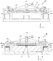
도 3 의 (A) 는, 도 2 의 계측 장치의 일부 생략한 정면도 (-Y 방향으로부터 본 도면), (B) 는, 마크 검출계의 광축 (AX1) 을 통과하는 XZ 평면으로 단면한 계측 장치의 일부 생략한 단면도이다.
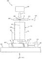
도 4 는 마크 검출계의 광축 (AX1) 을 통과하는 YZ 평면으로 단면한 계측 장치의 일부 생략한 단면도이다.
도 5 의 (A) 는, 제 1 위치 계측 시스템의 헤드부를 나타내는 사시도, (B) 는, 제 1 위치 계측 시스템의 헤드부의 평면도 (+Z 방향으로부터 본 도면) 이다.
도 6 은 제 2 위치 계측 시스템의 구성을 설명하기 위한 도면이다.
도 7 은 제 1 실시형태에 관련된 계측 장치의 제어계를 중심적으로 구성하는 제어 장치의 입출력 관계를 나타내는 블록도이다.
도 8 은 1 로트의 웨이퍼를 처리할 때의 제어 장치의 처리 알고리즘에 대응하는 플로우 차트이다.
도 9 는 도 1 에 나타내는 노광 장치의 구성을 개략적으로 나타내는 도면이다.
도 10 은 노광 장치가 구비하는 노광 제어 장치의 입출력 관계를 나타내는 블록도이다.
도 11 은 변형예에 관련된 리소그래피 시스템의 전체 구성을 개략적으로 나타내는 도면이다.
도 12 의 (A) 는, 고차 편미분 보정의 일례를 설명하기 위한 도면, (B) 는, 1 차 근사 보정의 일례를 설명하기 위한 도면이다.


12 : 정반
14 : 제진 장치
16 : 베이스 프레임
18 : 에어 베어링
20 : 구동 시스템
20A : 제 1 구동 장치
20B : 제 2 구동 장치
22a, 22b : 가동자
23a, 23b : 가동자
24 : 가동 스테이지
25a, 25b : 고정자
26a, 26b : 고정자
28A, 28B : X 축 리니어 모터
29A, 29B : Y 축 리니어 모터
30 : 제 1 위치 계측 시스템
32 : 헤드부
33 : 인코더 시스템
35a ∼ 35d : 레이저 간섭계
37x : X 헤드
37ya, 37yb : Y 헤드
40 : 계측 유닛
48 : 제진 장치
50 : 제 2 위치 계측 시스템
52A, 52B : 헤드부
58X1, 58X2 : XZ 헤드
58Y1, 58Y2 : YZ 헤드
60 : 제어 장치
100 : 계측 장치
100a, 100b : 계측 장치
200 : 노광 장치
300 : C/D
330 : 온조부
1000 : 리소그래피 시스템
MDS : 마크 검출계
RG1 : 그레이팅
RG2a, RG2b : 그레이팅
W : 웨이퍼
WST : 웨이퍼 스테이지
Claims (35)
- 적어도 1 개의 마크와 함께 구획 영역이 복수 형성된 기판을 처리 대상으로 하는 기판 처리 시스템으로서,
상기 기판을 유지 가능한 제 1 스테이지를 갖고, 그 제 1 스테이지에 유지된 상기 기판 상의 복수의 상기 마크의 위치 정보를 계측하는 계측 장치와,
상기 계측 장치에 의한 상기 복수의 마크의 위치 정보의 계측이 종료한 상기 기판이 재치되는 제 2 스테이지를 갖고, 그 제 2 스테이지 상에 재치된 상기 기판 상의 상기 복수의 마크 중 일부의 마크의 위치 정보를 계측하는 계측 동작 및 상기 복수의 구획 영역을 에너지 빔으로 노광하는 노광 동작을 실시하는 노광 장치를 구비하고,
상기 계측 장치는, 계측한 상기 복수의 마크의 상기 위치 정보를 사용하여, 상기 기판 상의 상기 복수의 구획 영역의 배열에 관한 제 1 정보를 구하고,
상기 노광 장치는, 계측한 상기 일부의 마크의 위치 정보를 사용하여, 상기 기판 상의 상기 복수의 구획 영역의 배열에 관한 제 2 정보를 구하고, 상기 계측 장치에서 구해진 상기 제 1 정보와, 상기 제 2 정보에 기초하여, 상기 노광 동작을 실시할 때에 상기 제 2 스테이지의 위치를 제어하는, 기판 처리 시스템. - 제 1 항에 있어서,
상기 제 1 정보는, 상기 기판 상의 상기 복수의 구획 영역의 배열의 비선형적인 변형 성분을 포함하는, 기판 처리 시스템. - 제 1 항 또는 제 2 항에 있어서,
상기 제 2 정보는, 상기 기판 상의 상기 복수의 구획 영역의 배열의 선형적인 변형 성분을 포함하는, 기판 처리 시스템. - 제 1 항 내지 제 3 항 중 어느 한 항에 있어서,
상기 계측 장치는, 상기 복수의 마크의 위치 정보를 사용하여, 상기 기판 상의 상기 복수의 구획 영역의 배열의 기준값에 대한 보정량의 관계를 제 1 소정차의 다항식으로 이루어지는 모델식으로 구하고,
상기 노광 장치는, 상기 일부의 마크의 위치 정보를 사용하여, 상기 기판 상의 상기 복수의 구획 영역의 배열의 기준값에 대한 보정량의 관계를 제 2 소정차의 다항식으로 이루어지는 모델식으로 구하는, 기판 처리 시스템. - 제 4 항에 있어서,
상기 복수의 구획 영역은, 상기 기판 상에 매트릭스상의 배치로 형성되고, 상기 복수의 구획 영역의 배열의 상기 보정량은, 상기 기판 상의 소정의 기준점을 원점으로 하고, 상기 매트릭스의 행 방향인 X 축 방향과 열 방향인 Y 축 방향을 축 방향으로 하는 2 차원 직교 좌표계인 기판 좌표계에 있어서의 각 구획 영역의 설계상의 위치 좌표 X, Y 와, 그 구획 영역의 위치 좌표의 보정량의 관계를 나타내는, X, Y 에 관한 다항식으로 이루어지는 모델식에 기초하여 구해지고,
상기 계측 장치는, 통계 연산에 의해 상기 모델식의 고차항의 계수를 구하고,
상기 노광 장치는, 통계 연산에 의해, 상기 모델식의 저차항의 계수를 구하고, 그 저차항의 계수와 상기 고차항의 계수가, 상기 모델식에 대입된 계수 확정 후의 모델식에 기초하여 상기 기판 상의 상기 복수의 구획 영역의 배열의 상기 보정량을 구하는, 기판 처리 시스템. - 제 5 항에 있어서,
상기 저차항은, 1 차 이하의 항이고, 상기 고차항은 2 차 이상의 항인, 기판 처리 시스템. - 제 5 항 또는 제 6 항에 있어서,
상기 노광 장치는, 상기 계수 확정 후의 모델식을, X, Y 에 대해 편미분한 값에 따라 상기 복수의 구획 영역의 변형을 추정하는, 기판 처리 시스템. - 제 5 항에 있어서,
상기 노광 장치는, 상기 구한 보정량과 상기 기판 상의 상기 복수의 구획 영역의 배열의 설계값에 기초하여, 상기 기판 상의 상기 복수의 구획 영역의 배열인 그리드를 구하고, 그 그리드를, 1 차의 모델식에 근사하고, 그 모델식의 계수에 따라, 상기 복수의 구획 영역의 변형을 추정하는, 기판 처리 시스템. - 제 7 항 또는 제 8 항에 있어서,
상기 노광 장치는, 패턴이 형성된 마스크를 유지하는 마스크 스테이지와 상기 제 2 스테이지를 동기하여 투영 광학계에 대해 상대 이동시키고, 상기 패턴을 상기 기판 상의 상기 구획 영역에 전사하는 주사 노광을 실시하는 장치이고,
상기 노광 장치는, 상기 추정된 상기 구획 영역의 변형 후의 형상에 맞춰 상기 패턴의 상기 투영 광학계에 의한 투영 이미지가 변형되도록, 상기 주사 노광 중에, 상기 마스크 스테이지와 상기 제 2 스테이지의 상대 주사 각도, 주사 속도비, 상기 마스크 스테이지 및 상기 제 2 스테이지의 적어도 일방의 상기 투영 광학계에 대한 상대 위치, 상기 투영 광학계의 결상 특성, 및 노광광의 파장 중 적어도 1 개를 조정하는, 기판 처리 시스템. - 제 1 항 내지 제 9 항 중 어느 한 항에 있어서,
상기 계측 장치는, 상기 제 1 스테이지에 유지된 상기 기판 상의 상기 마크를 검출하고, 검출 신호를 출력하는 마크 검출계와, 상기 마크 검출계에 대한 상기 제 1 스테이지의 위치 정보를 계측하는 위치 계측 장치와, 상기 제 1 스테이지를 구동하는 구동 시스템과, 상기 위치 계측 장치에서 계측된 상기 위치 정보에 기초하여, 상기 구동 시스템에 의한 상기 제 1 스테이지의 구동을 제어하면서, 상기 위치 계측 장치에 의한 상기 위치 정보를 취득하고, 상기 마크 검출계를 사용하여 상기 제 1 스테이지에 유지된 상기 기판 상의 상기 복수의 마크의 위치 정보를 구하는 제어 장치를 구비하는, 기판 처리 시스템. - 제 10 항에 있어서,
상기 제 1 스테이지는, 베이스 부재에 대해 이동 가능하고,
상기 위치 계측 장치는, 상기 베이스 부재에 대한 상기 스테이지의 제 1 위치 정보를 계측하는 제 1 위치 계측계와, 상기 마크 검출계와 상기 베이스 부재의 상대적인 제 2 위치 정보를 계측하는 제 2 위치 계측계를 포함하는, 기판 처리 시스템. - 제 11 항에 있어서,
상기 제 1 위치 계측계는, 격자부를 갖는 계측면과 상기 계측면에 빔을 조사하는 헤드부의 일방이 상기 제 1 스테이지에 설치되고, 상기 헤드부로부터의 복수의 빔을 상기 계측면에 조사하고, 상기 복수의 빔 각각의 상기 계측면으로부터의 복귀 빔을 수광하여 상기 제 1 스테이지의 제 1 위치 정보를 계측하는, 기판 처리 시스템. - 제 10 항 내지 제 12 항 중 어느 한 항에 있어서,
상기 계측 장치는, 상기 마크 검출계에 의한 검출 조건이 서로 상이한 복수의 계측 모드를 설정 가능한, 기판 처리 시스템. - 제 13 항에 있어서,
상기 복수의 계측 모드에는, 상기 기판 상의 모든 구획 영역에 대해 각 1 개의 마크를 검출 대상으로 하는 제 1 모드와, 상기 기판 상의 모든 구획 영역에 대해 각 2 개 이상의 제 1 수의 마크를 검출하는 제 2 모드와, 상기 기판 상의 일부의 구획 영역에 대해서는 2 개 이상의 제 2 수의 마크를 검출하고, 나머지 구획 영역에 대해서는 각 1 개의 마크를 검출하는 제 3 모드 중 적어도 1 개의 모드가 포함되는, 기판 처리 시스템. - 제 13 항 또는 제 14 항에 있어서,
상기 복수의 계측 모드에는, 복수장의 기판을 연속적으로 처리할 때에, 최초로 처리되는 제 1 장째의 기판을 포함하는 소정 장수의 기판의 계측 결과에 따라, 상기 복수의 모드 중 하나의 모드를 설정하는 제 4 모드가 포함되는, 기판 처리 시스템. - 제 13 항 또는 제 14 항에 있어서,
상기 복수의 계측 모드에는, 복수장의 기판을 연속적으로 처리할 때에, 최초로 처리되는 제 1 장째의 기판을 포함하는 소정 장수의 기판의 계측 결과에 기초하여, 나머지 기판에 대해 상기 마크 검출계에 의한 검출의 대상이 되는 마크를 결정하는 모드가 포함되는, 기판 처리 시스템. - 제 13 항 내지 제 16 항 중 어느 한 항에 있어서,
상기 계측 장치에 의해 상기 기판 상의 복수의 구획 영역 중 적어도 일부의 구획 영역에 대해, 복수의 상기 마크의 위치 정보가 계측된 경우,
상기 노광 장치는, 상기 계측 동작을 실시할 때에, 상기 기판 상의 상기 적어도 일부의 구획 영역에 대해 상기 계측 장치에 의해 위치 정보가 계측된 상기 복수의 마크를 포함하는, 상기 기판 상의 복수의 마크 중에서 선택한 복수의 마크의 위치 정보를 계측하고, 그 계측한 복수의 마크의 위치 정보를 사용하여 상기 통계 연산을 포함하는 연산을 실시하고, 상기 구획 영역의 변형을 추정하는, 기판 처리 시스템. - 제 1 항 내지 제 17 항 중 어느 한 항에 있어서,
상기 계측 장치와 상기 노광 장치는, 인라인으로 접속되어 있는, 기판 처리 시스템. - 제 18 항에 있어서,
상기 계측 장치 및 상기 노광 장치에 인라인 접속되고, 상기 기판에 소정 처리를 실시하는 기판 처리 장치를 추가로 구비하는, 기판 처리 시스템. - 제 19 항에 있어서,
상기 기판 처리 장치는, 기판 상에 감응제를 도포하는 도포 장치인, 기판 처리 시스템. - 제 19 항에 있어서,
상기 기판 처리 장치는, 기판 상에 감응제를 도포함과 함께, 노광 후의 상기 기판을 현상하는 도포 현상 장치인, 기판 처리 시스템. - 제 20 항 또는 제 21 항에 있어서,
상기 계측 장치는, 상기 노광 장치와 상기 기판 처리 장치 사이에 배치되는, 기판 처리 시스템. - 제 20 항 내지 제 22 항 중 어느 한 항에 있어서,
상기 계측 장치는, 상기 감응제가 도포되기 전의 기판 상의 복수의 마크의 위치 정보의 계측을 실시하는 사전 계측과, 상기 감응제가 도포된 상기 기판 상의 상기 복수의 마크의 위치 정보의 계측을 실시하는 사후 계측의 적어도 일방에서 사용되는, 기판 처리 시스템. - 제 20 항 또는 제 21 항에 있어서,
상기 계측 장치는, 복수 설치되고, 그 복수의 계측 장치 중 제 1 계측 장치와 제 2 계측 장치는, 상기 노광 장치와 상기 기판 처리 장치 사이에 배치되고,
상기 제 1 계측 장치 및 상기 제 2 계측 장치는, 상기 감응제가 도포되기 전의 기판 상의 복수의 마크의 위치 정보의 계측을 실시하는 사전 계측과, 상기 감응제가 도포된 상기 기판 상의 상기 복수의 마크의 위치 정보의 계측을 실시하는 사후 계측 양방에서 사용되고,
상기 제 1 계측 장치와 상기 제 2 계측 장치는, 복수장의 기판을 연속 처리할 때에, 모두 동일 기판에 대한 상기 사전 계측과 상기 사후 계측에서 사용되는, 기판 처리 시스템. - 제 20 항 또는 제 21 항에 있어서,
상기 계측 장치는, 복수 설치되고, 상기 복수의 계측 장치 중 제 1 계측 장치는, 상기 노광 장치와 상기 기판 처리 장치 사이에 배치되고, 상기 복수의 계측 장치 중 제 2 계측 장치는, 상기 기판 처리 장치를 사이에 두고 상기 노광 장치의 반대측에 배치되고,
상기 제 2 계측 장치는, 상기 감응제가 도포되기 전의 기판 상의 복수의 마크의 위치 정보의 계측을 실시하는 사전 계측에 사용되고,
상기 제 1 계측 장치는, 상기 감응제가 도포된 상기 기판 상의 상기 복수의 마크의 위치 정보의 계측을 실시하는 사후 계측에 사용되는, 기판 처리 시스템. - 제 19 항에 있어서,
상기 기판 처리 장치는, 노광 후의 상기 기판을 현상하는 현상 장치인, 기판 처리 시스템. - 제 26 항에 있어서,
상기 계측 장치는, 상기 노광 장치와 상기 기판 처리 장치 사이에 배치되는, 기판 처리 시스템. - 제 21 항, 제 26 항 또는 제 27 항 중 어느 한 항에 있어서,
상기 계측 장치는, 상기 감응제가 도포된 상기 기판 상의 상기 복수의 마크의 위치 정보의 계측을 실시하는 사후 계측과, 현상 종료 후의 상기 기판 상의 중첩 어긋남 계측 마크의 위치 어긋남량을 계측하는 중첩 어긋남 계측 양방에서 사용되는, 기판 처리 시스템. - 제 21 항, 제 26 항 또는 제 27 항 중 어느 한 항에 있어서,
상기 계측 장치는, 복수 설치되고, 그 복수의 계측 장치 중 제 1 계측 장치는, 상기 노광 장치와 상기 기판 처리 장치 사이에 배치되고, 나머지 계측 장치 중 제 2 계측 장치는, 상기 기판 처리 장치를 사이에 두고 상기 노광 장치의 반대측에 배치되고,
상기 제 1 계측 장치는, 상기 감응제가 도포된 상기 기판 상의 상기 복수의 마크의 위치 정보의 계측을 실시하는 사후 계측에 사용되고,
상기 제 2 계측 장치는, 현상 종료 후의 상기 기판 상의 중첩 어긋남 계측 마크의 위치 어긋남량을 계측하는 중첩 어긋남 계측에 사용되는, 기판 처리 시스템. - 제 19 항 내지 제 29 항 중 어느 한 항에 있어서,
상기 계측 장치의 상기 스테이지에 탑재되는 데에 앞서, 소정의 온도 범위 내가 되도록 상기 기판을 온조하는 온조 장치를 추가로 구비하는, 기판 처리 시스템. - 제 30 항에 있어서,
상기 온조 장치는, 상기 기판 처리 장치의 일부에 설치되는, 기판 처리 시스템. - 제 1 항 내지 제 31 항 중 어느 한 항에 기재된 기판 처리 시스템을 사용하여 기판을 노광하는 것과,
노광된 상기 기판을 현상하는 것을 포함하는, 디바이스 제조 방법. - 적어도 1 개의 마크와 함께 구획 영역이 복수 형성된 기판을 처리 대상으로 하는 기판 처리 방법으로서,
제 1 스테이지에 유지된 상기 기판 상의 복수의 상기 마크의 위치 정보를 계측하는 것과,
상기 계측하는 것으로 상기 복수의 마크의 위치 정보의 계측이 종료한 상기 기판을, 제 2 스테이지에 유지시키고, 그 제 2 스테이지에 유지된 상기 기판 상의 상기 복수의 마크 중 일부의 마크의 위치 정보를 계측하는 계측 동작 및 상기 복수의 구획 영역을 에너지 빔으로 노광하는 노광 동작을 실시하는 것을 포함하고,
상기 계측하는 것으로는, 계측한 상기 복수의 마크의 상기 위치 정보를 사용하여, 상기 기판 상의 상기 복수의 구획 영역의 배열에 관한 제 1 정보를 구하고,
상기 계측 동작 및 노광 동작을 실시하는 것으로는, 계측한 상기 일부의 마크의 위치 정보를 사용하여, 상기 기판 상의 상기 복수의 구획 영역의 배열에 관한 제 2 정보를 구하고, 상기 계측하는 것으로 구해진 상기 제 1 정보와, 상기 제 2 정보에 기초하여, 상기 노광 동작을 실시할 때에 상기 제 2 스테이지의 위치를 제어하는, 기판 처리 방법. - 제 33 항에 있어서,
상기 복수의 구획 영역은, 상기 기판 상에 매트릭스상의 배치로 형성되고, 상기 복수의 구획 영역의 배열의 기준값에 대한 보정량은, 상기 기판 상의 소정의 기준점을 원점으로 하고, 상기 매트릭스의 행 방향인 X 축 방향과 열 방향인 Y 축 방향을 축 방향으로 하는 2 차원 직교 좌표계인 기판 좌표계에 있어서의 각 구획 영역의 설계상의 위치 좌표 X, Y 와, 그 구획 영역의 위치 좌표의 보정량의 관계를 나타내는, X, Y 에 관한 다항식으로 이루어지는 모델식에 기초하여 구해지고,
상기 계측하는 것으로는, 상기 통계 연산에 의해 상기 모델식의 고차항의 계수를 구하고,
상기 계측 동작 및 노광 동작을 실시하는 것으로는, 상기 통계 연산에 의해 상기 모델식의 저차항의 계수를 구하고, 그 저차항의 계수와 상기 고차항의 계수가, 상기 모델식에 대입된 계수 확정 후의 모델식에 기초하여 상기 기판 상의 상기 복수의 구획 영역의 배열의 상기 보정량을 구하는, 기판 처리 방법. - 제 34 항에 있어서,
상기 저차항은 1 차 이하의 항이고, 상기 고차항은 2 차 이상의 항인, 기판 처리 방법.
Priority Applications (1)
| Application Number | Priority Date | Filing Date | Title |
|---|---|---|---|
| KR1020247001253A KR102873223B1 (ko) | 2015-02-23 | 2016-02-23 | 기판 처리 시스템 및 기판 처리 방법, 그리고 디바이스 제조 방법 |
Applications Claiming Priority (3)
| Application Number | Priority Date | Filing Date | Title |
|---|---|---|---|
| JPJP-P-2015-032911 | 2015-02-23 | ||
| JP2015032911 | 2015-02-23 | ||
| PCT/JP2016/055133 WO2016136691A1 (ja) | 2015-02-23 | 2016-02-23 | 基板処理システム及び基板処理方法、並びにデバイス製造方法 |
Related Child Applications (1)
| Application Number | Title | Priority Date | Filing Date |
|---|---|---|---|
| KR1020247001253A Division KR102873223B1 (ko) | 2015-02-23 | 2016-02-23 | 기판 처리 시스템 및 기판 처리 방법, 그리고 디바이스 제조 방법 |
Publications (2)
| Publication Number | Publication Date |
|---|---|
| KR20170118210A true KR20170118210A (ko) | 2017-10-24 |
| KR102632657B1 KR102632657B1 (ko) | 2024-02-01 |
Family
ID=56788752
Family Applications (3)
| Application Number | Title | Priority Date | Filing Date |
|---|---|---|---|
| KR1020247001253A Active KR102873223B1 (ko) | 2015-02-23 | 2016-02-23 | 기판 처리 시스템 및 기판 처리 방법, 그리고 디바이스 제조 방법 |
| KR1020257034249A Pending KR20250156187A (ko) | 2015-02-23 | 2016-02-23 | 기판 처리 시스템 및 기판 처리 방법, 그리고 디바이스 제조 방법 |
| KR1020177026406A Active KR102632657B1 (ko) | 2015-02-23 | 2016-02-23 | 기판 처리 시스템 및 기판 처리 방법, 그리고 디바이스 제조 방법 |
Family Applications Before (2)
| Application Number | Title | Priority Date | Filing Date |
|---|---|---|---|
| KR1020247001253A Active KR102873223B1 (ko) | 2015-02-23 | 2016-02-23 | 기판 처리 시스템 및 기판 처리 방법, 그리고 디바이스 제조 방법 |
| KR1020257034249A Pending KR20250156187A (ko) | 2015-02-23 | 2016-02-23 | 기판 처리 시스템 및 기판 처리 방법, 그리고 디바이스 제조 방법 |
Country Status (8)
| Country | Link |
|---|---|
| US (4) | US10775708B2 (ko) |
| EP (2) | EP3264180B1 (ko) |
| JP (5) | JP6719729B2 (ko) |
| KR (3) | KR102873223B1 (ko) |
| CN (4) | CN111948912A (ko) |
| HK (1) | HK1246872A1 (ko) |
| TW (3) | TWI840811B (ko) |
| WO (1) | WO2016136691A1 (ko) |
Families Citing this family (21)
| Publication number | Priority date | Publication date | Assignee | Title |
|---|---|---|---|---|
| CN111176083B (zh) | 2015-02-23 | 2023-07-28 | 株式会社尼康 | 测量装置、光刻系统、曝光装置、测量方法以及曝光方法 |
| CN111948912A (zh) | 2015-02-23 | 2020-11-17 | 株式会社尼康 | 基板处理系统及基板处理方法、以及组件制造方法 |
| KR102552792B1 (ko) * | 2015-02-23 | 2023-07-06 | 가부시키가이샤 니콘 | 계측 장치, 리소그래피 시스템 및 노광 장치, 그리고 디바이스 제조 방법 |
| KR102625369B1 (ko) | 2016-09-30 | 2024-01-15 | 가부시키가이샤 니콘 | 계측 시스템 및 기판 처리 시스템, 그리고 디바이스 제조 방법 |
| DE102016225899A1 (de) * | 2016-12-21 | 2018-06-21 | Carl Zeiss Smt Gmbh | Verfahren und Vorrichtung zum Modifizieren von Abbildungseigenschaften eines optischen Systems für die Mikrolithographie |
| CN110268334B (zh) * | 2017-02-03 | 2024-10-29 | Asml荷兰有限公司 | 曝光设备 |
| JP6942555B2 (ja) * | 2017-08-03 | 2021-09-29 | 東京エレクトロン株式会社 | 基板処理方法、コンピュータ記憶媒体及び基板処理システム |
| EP3531206A1 (en) * | 2018-02-23 | 2019-08-28 | ASML Netherlands B.V. | Systems and methods for improving resist model predictions |
| CN108899288B (zh) * | 2018-07-20 | 2020-11-13 | 上海华虹宏力半导体制造有限公司 | 晶圆标记的监控方法和激光刻号机台对准位置的判定方法 |
| US11408734B2 (en) * | 2019-01-03 | 2022-08-09 | Lam Research Corporation | Distance measurement between gas distribution device and substrate support at high temperatures |
| US11764111B2 (en) * | 2019-10-24 | 2023-09-19 | Texas Instruments Incorporated | Reducing cross-wafer variability for minimum width resistors |
| US11204312B2 (en) * | 2020-03-13 | 2021-12-21 | Applied Materials, Inc. | In-situ full wafer metrology system |
| CN115039032B (zh) * | 2020-03-19 | 2026-02-17 | 极光先进雷射株式会社 | 曝光系统、激光控制参数的生成方法和电子器件的制造方法 |
| JP7463154B2 (ja) * | 2020-03-24 | 2024-04-08 | 株式会社Screenホールディングス | 描画装置、データ処理装置、描画方法、および描画データ生成方法 |
| TWI746318B (zh) * | 2020-12-17 | 2021-11-11 | 萬潤科技股份有限公司 | 檢測方法、檢測裝置及設備 |
| CN112631080B (zh) * | 2020-12-21 | 2022-05-31 | 苏州源卓光电科技有限公司 | 一种双工作台曝光机的曝光方法 |
| JP7689430B2 (ja) * | 2021-02-18 | 2025-06-06 | 東洋鋼鈑株式会社 | 測定装置 |
| JP7625950B2 (ja) | 2021-04-12 | 2025-02-04 | 株式会社ニコン | 露光装置、露光方法、デバイス製造方法、及びデバイス |
| JP7649188B2 (ja) | 2021-04-21 | 2025-03-19 | キヤノン株式会社 | 処理システム、計測装置、基板処理装置及び物品の製造方法 |
| JP7840203B2 (ja) * | 2022-04-20 | 2026-04-03 | 株式会社日立ハイテク | ステージ装置、荷電粒子線装置、及び光学式検査装置 |
| JP2025024503A (ja) | 2023-08-07 | 2025-02-20 | キヤノン株式会社 | 位置決め方法、基板処理方法、物品製造方法、位置決め装置、および基板処理装置 |
Citations (6)
| Publication number | Priority date | Publication date | Assignee | Title |
|---|---|---|---|---|
| KR20010109212A (ko) * | 2000-05-31 | 2001-12-08 | 시마무라 테루오 | 평가방법, 위치검출방법, 노광방법 및 디바이스 제조방법,및 노광장치 |
| KR20020042664A (ko) | 1999-09-10 | 2002-06-05 | 그래탐 두드렌 스웨트맨 | 내고온성 염수용해성 섬유 |
| KR20080096520A (ko) * | 2006-01-26 | 2008-10-30 | 가부시키가이샤 니콘 | 중첩 관리 방법 및 장치, 처리 장치, 측정 장치 및 노광장치, 디바이스 제조 시스템 및 디바이스 제조 방법, 및프로그램 및 정보 기록 매체 |
| US20090111060A1 (en) * | 2007-10-31 | 2009-04-30 | Nanya Technology Corporation | Exposure method |
| JP2009117491A (ja) * | 2007-11-02 | 2009-05-28 | Canon Inc | 位置合わせ方法、位置合わせ装置、露光方法、露光装置及びデバイス製造方法 |
| KR20140107186A (ko) * | 2011-12-29 | 2014-09-04 | 가부시키가이샤 니콘 | 노광 장치, 노광 방법 및 디바이스 제조 방법 |
Family Cites Families (199)
| Publication number | Priority date | Publication date | Assignee | Title |
|---|---|---|---|---|
| US4780617A (en) | 1984-08-09 | 1988-10-25 | Nippon Kogaku K.K. | Method for successive alignment of chip patterns on a substrate |
| US4734746A (en) * | 1985-06-24 | 1988-03-29 | Nippon Kogaku K. K. | Exposure method and system for photolithography |
| JP2897355B2 (ja) | 1990-07-05 | 1999-05-31 | 株式会社ニコン | アライメント方法,露光装置,並びに位置検出方法及び装置 |
| JP3261793B2 (ja) * | 1993-03-19 | 2002-03-04 | 株式会社ニコン | 位置合わせ方法、及び露光方法 |
| KR100300618B1 (ko) | 1992-12-25 | 2001-11-22 | 오노 시게오 | 노광방법,노광장치,및그장치를사용하는디바이스제조방법 |
| US20010049589A1 (en) | 1993-01-21 | 2001-12-06 | Nikon Corporation | Alignment method and apparatus therefor |
| JP3412704B2 (ja) | 1993-02-26 | 2003-06-03 | 株式会社ニコン | 投影露光方法及び装置、並びに露光装置 |
| US5461237A (en) | 1993-03-26 | 1995-10-24 | Nikon Corporation | Surface-position setting apparatus |
| JP3448614B2 (ja) * | 1993-08-12 | 2003-09-22 | 株式会社ニコン | 投影露光方法、走査型投影露光装置、及び素子製造方法 |
| JP3326902B2 (ja) * | 1993-09-10 | 2002-09-24 | 株式会社日立製作所 | パターン検出方法及びパターン検出装置及びそれを用いた投影露光装置 |
| JPH07270122A (ja) * | 1994-03-30 | 1995-10-20 | Canon Inc | 変位検出装置、該変位検出装置を備えた露光装置およびデバイスの製造方法 |
| US6989647B1 (en) | 1994-04-01 | 2006-01-24 | Nikon Corporation | Positioning device having dynamically isolated frame, and lithographic device provided with such a positioning device |
| JPH07307269A (ja) * | 1994-05-13 | 1995-11-21 | Canon Inc | 位置合わせ方法 |
| JPH08115869A (ja) * | 1994-10-18 | 1996-05-07 | Nikon Corp | 位置合わせ方法 |
| KR100500199B1 (ko) * | 1995-05-29 | 2005-11-01 | 가부시키가이샤 니콘 | 마스크패턴을겹쳐서노광하는노광방법 |
| JP3634487B2 (ja) * | 1996-02-09 | 2005-03-30 | キヤノン株式会社 | 位置合せ方法、位置合せ装置、および露光装置 |
| JP3884098B2 (ja) * | 1996-03-22 | 2007-02-21 | 株式会社東芝 | 露光装置および露光方法 |
| JPH09289149A (ja) | 1996-04-23 | 1997-11-04 | Fujitsu Ltd | X線マスク及びその製造方法 |
| SG102627A1 (en) | 1996-11-28 | 2004-03-26 | Nikon Corp | Lithographic device |
| WO1998028665A1 (en) | 1996-12-24 | 1998-07-02 | Koninklijke Philips Electronics N.V. | Two-dimensionally balanced positioning device with two object holders, and lithographic device provided with such a positioning device |
| JPH10335239A (ja) * | 1997-05-30 | 1998-12-18 | Canon Inc | 露光方法及び露光装置 |
| WO1999028220A1 (en) | 1997-12-03 | 1999-06-10 | Nikon Corporation | Substrate transferring device and method |
| US6208407B1 (en) | 1997-12-22 | 2001-03-27 | Asm Lithography B.V. | Method and apparatus for repetitively projecting a mask pattern on a substrate, using a time-saving height measurement |
| JPH11191585A (ja) | 1997-12-26 | 1999-07-13 | Canon Inc | ステージ装置、およびこれを用いた露光装置、ならびにデバイス製造方法 |
| US6924884B2 (en) * | 1999-03-08 | 2005-08-02 | Asml Netherlands B.V. | Off-axis leveling in lithographic projection apparatus |
| US6771350B2 (en) | 2000-02-25 | 2004-08-03 | Nikon Corporation | Exposure apparatus and exposure method capable of controlling illumination distribution |
| JP2001274073A (ja) | 2000-03-28 | 2001-10-05 | Toshiba Corp | 重ね合わせ露光方法及び露光システム |
| JP2001297966A (ja) * | 2000-04-13 | 2001-10-26 | Canon Inc | 露光方法、露光システム、露光装置、半導体デバイス製造方法、半導体製造工場、および露光装置の保守方法 |
| US20020041377A1 (en) | 2000-04-25 | 2002-04-11 | Nikon Corporation | Aerial image measurement method and unit, optical properties measurement method and unit, adjustment method of projection optical system, exposure method and apparatus, making method of exposure apparatus, and device manufacturing method |
| JP2001345243A (ja) * | 2000-05-31 | 2001-12-14 | Nikon Corp | 評価方法、位置検出方法、露光方法及びデバイス製造方法 |
| JP4915033B2 (ja) * | 2000-06-15 | 2012-04-11 | 株式会社ニコン | 露光装置、基板処理装置及びリソグラフィシステム、並びにデバイス製造方法 |
| US20030020889A1 (en) | 2000-08-02 | 2003-01-30 | Nikon Corporation | Stage unit, measurement unit and measurement method, and exposure apparatus and exposure method |
| US7561270B2 (en) * | 2000-08-24 | 2009-07-14 | Asml Netherlands B.V. | Lithographic apparatus, device manufacturing method and device manufactured thereby |
| JP2002231622A (ja) * | 2000-11-29 | 2002-08-16 | Nikon Corp | ステージ装置及び露光装置 |
| US20020109823A1 (en) | 2001-02-09 | 2002-08-15 | Nikon Corporation. | Wafer stage assembly |
| JP3762307B2 (ja) | 2001-02-15 | 2006-04-05 | キヤノン株式会社 | レーザ干渉干渉計システムを含む露光装置 |
| JP2003017386A (ja) | 2001-06-29 | 2003-01-17 | Canon Inc | 位置合わせ方法、露光方法、露光装置及びデバイスの製造方法 |
| JP2003124094A (ja) * | 2001-10-10 | 2003-04-25 | Canon Inc | 露光装置の制御方法及び露光システム |
| JP3966211B2 (ja) | 2002-05-08 | 2007-08-29 | 株式会社ニコン | 露光方法、露光装置及びデバイス製造方法 |
| TW541642B (en) * | 2002-05-10 | 2003-07-11 | Nanya Technology Corp | Wafer alignment method |
| EP1420298B1 (en) | 2002-11-12 | 2013-02-20 | ASML Netherlands B.V. | Lithographic apparatus |
| KR100585476B1 (ko) | 2002-11-12 | 2006-06-07 | 에이에스엠엘 네델란즈 비.브이. | 리소그래피 장치 및 디바이스 제조방법 |
| ATE424026T1 (de) | 2002-12-13 | 2009-03-15 | Koninkl Philips Electronics Nv | Flüssigkeitsentfernung in einem verfahren und einer einrichtung zum bestrahlen von flecken auf einer schicht |
| EP1732075A3 (en) | 2002-12-19 | 2007-02-21 | Koninklijke Philips Electronics N.V. | Method and device for irradiating spots on a layer |
| EP2466621B1 (en) | 2003-02-26 | 2015-04-01 | Nikon Corporation | Exposure apparatus, exposure method, and method for producing device |
| JP2004260117A (ja) * | 2003-02-27 | 2004-09-16 | Nikon Corp | ステージ装置、露光装置、及びデバイス製造方法 |
| JP4164414B2 (ja) | 2003-06-19 | 2008-10-15 | キヤノン株式会社 | ステージ装置 |
| JP2005086093A (ja) * | 2003-09-10 | 2005-03-31 | Canon Inc | 露光装置及びステージ装置の制御方法 |
| WO2005029559A1 (ja) | 2003-09-19 | 2005-03-31 | Nikon Corporation | 露光装置及びデバイス製造方法 |
| US7443511B2 (en) | 2003-11-25 | 2008-10-28 | Asml Netherlands B.V. | Integrated plane mirror and differential plane mirror interferometer system |
| WO2005053007A1 (ja) | 2003-11-28 | 2005-06-09 | Nikon Corporation | 露光方法及びデバイス製造方法、露光装置、並びにプログラム |
| US7589822B2 (en) * | 2004-02-02 | 2009-09-15 | Nikon Corporation | Stage drive method and stage unit, exposure apparatus, and device manufacturing method |
| US7102729B2 (en) | 2004-02-03 | 2006-09-05 | Asml Netherlands B.V. | Lithographic apparatus, measurement system, and device manufacturing method |
| JP4429037B2 (ja) | 2004-02-27 | 2010-03-10 | キヤノン株式会社 | ステージ装置及びその制御方法 |
| JP4760705B2 (ja) * | 2004-03-01 | 2011-08-31 | 株式会社ニコン | 事前計測処理方法、露光システム及び基板処理装置 |
| US7728953B2 (en) | 2004-03-01 | 2010-06-01 | Nikon Corporation | Exposure method, exposure system, and substrate processing apparatus |
| TW200605191A (en) * | 2004-03-30 | 2006-02-01 | Nikon Corp | Exposure apparatus, exposure method, device manufacturing method, and surface shape detecting device |
| JP4751032B2 (ja) | 2004-04-22 | 2011-08-17 | 株式会社森精機製作所 | 変位検出装置 |
| JP2005322755A (ja) * | 2004-05-07 | 2005-11-17 | Nikon Corp | 誤差検出方法、位置合わせ方法、露光方法 |
| JP2005327993A (ja) | 2004-05-17 | 2005-11-24 | Canon Inc | 位置決め装置、露光装置及びデバイス製造方法 |
| JP2005337912A (ja) | 2004-05-27 | 2005-12-08 | Nikon Corp | 位置計測装置、露光装置、及びデバイスの製造方法 |
| JP4678372B2 (ja) | 2004-06-29 | 2011-04-27 | 株式会社ニコン | 管理方法及び管理システム、並びにプログラム |
| US7256871B2 (en) | 2004-07-27 | 2007-08-14 | Asml Netherlands B.V. | Lithographic apparatus and method for calibrating the same |
| TW200615716A (en) * | 2004-08-05 | 2006-05-16 | Nikon Corp | Stage device and exposure device |
| WO2006025386A1 (ja) | 2004-08-31 | 2006-03-09 | Nikon Corporation | 位置合わせ方法、処理システム、基板の投入再現性計測方法、位置計測方法、露光方法、基板処理装置、計測方法及び計測装置 |
| EP1804278A4 (en) | 2004-09-14 | 2011-03-02 | Nikon Corp | CORRECTION METHOD AND EXPOSURE DEVICE |
| JP3962736B2 (ja) * | 2004-10-08 | 2007-08-22 | キヤノン株式会社 | 露光装置およびデバイス製造方法 |
| TWI654661B (zh) * | 2004-11-18 | 2019-03-21 | Nikon Corporation | 位置測量方法、位置控制方法、測量方法、裝載方法、曝光方法及曝光裝置、及元件製造方法 |
| US20060139595A1 (en) | 2004-12-27 | 2006-06-29 | Asml Netherlands B.V. | Lithographic apparatus and method for determining Z position errors/variations and substrate table flatness |
| TWI402890B (zh) * | 2005-01-24 | 2013-07-21 | 尼康股份有限公司 | Measurement methods, measurement systems, inspection methods, inspection systems, exposure methods and exposure systems |
| JP2006222312A (ja) * | 2005-02-10 | 2006-08-24 | Canon Inc | ステージ制御装置及びその方法、ステージ装置並びに露光装置 |
| US7161659B2 (en) * | 2005-04-08 | 2007-01-09 | Asml Netherlands B.V. | Dual stage lithographic apparatus and device manufacturing method |
| US7515281B2 (en) * | 2005-04-08 | 2009-04-07 | Asml Netherlands B.V. | Lithographic apparatus and device manufacturing method |
| US7405811B2 (en) | 2005-04-20 | 2008-07-29 | Asml Netherlands B.V. | Lithographic apparatus and positioning apparatus |
| US7838858B2 (en) | 2005-05-31 | 2010-11-23 | Nikon Corporation | Evaluation system and method of a search operation that detects a detection subject on an object |
| EP1744217B1 (en) | 2005-07-12 | 2012-03-14 | ASML Netherlands B.V. | Method of selecting a grid model for correcting grid deformations in a lithographic apparatus and lithographic assembly using the same |
| US7348574B2 (en) | 2005-09-02 | 2008-03-25 | Asml Netherlands, B.V. | Position measurement system and lithographic apparatus |
| DE102005043569A1 (de) | 2005-09-12 | 2007-03-22 | Dr. Johannes Heidenhain Gmbh | Positionsmesseinrichtung |
| US7362446B2 (en) | 2005-09-15 | 2008-04-22 | Asml Netherlands B.V. | Position measurement unit, measurement system and lithographic apparatus comprising such position measurement unit |
| WO2007043535A1 (ja) | 2005-10-07 | 2007-04-19 | Nikon Corporation | 光学特性計測方法、露光方法及びデバイス製造方法、並びに検査装置及び計測方法 |
| JP2007115784A (ja) * | 2005-10-18 | 2007-05-10 | Nikon Corp | 露光システム、露光方法、及びデバイス製造工場 |
| JP5061904B2 (ja) * | 2005-10-28 | 2012-10-31 | 株式会社ニコン | デバイス製造処理装置間の接続装置及び接続方法、プログラム、デバイス製造処理システム、露光装置及び露光方法、並びに測定検査装置及び測定検査方法 |
| JP4840684B2 (ja) * | 2005-11-04 | 2011-12-21 | 株式会社ニコン | 露光方法 |
| WO2007052699A1 (ja) * | 2005-11-04 | 2007-05-10 | Nikon Corporation | 解析装置、処理装置、測定装置、露光装置、基板処理システム、解析方法及びプログラム |
| TWI457977B (zh) | 2005-12-28 | 2014-10-21 | 尼康股份有限公司 | A pattern forming method and a pattern forming apparatus, and an element manufacturing method |
| US8411271B2 (en) * | 2005-12-28 | 2013-04-02 | Nikon Corporation | Pattern forming method, pattern forming apparatus, and device manufacturing method |
| JP2007184343A (ja) | 2006-01-05 | 2007-07-19 | Nikon Corp | 処理方法、処理装置、及びプログラム |
| JP2007184342A (ja) * | 2006-01-05 | 2007-07-19 | Nikon Corp | 露光システム、露光方法、及びデバイス製造方法 |
| KR101323565B1 (ko) | 2006-01-19 | 2013-10-29 | 가부시키가이샤 니콘 | 이동체 구동 방법 및 이동체 구동 시스템, 패턴 형성 방법및 패턴 형성 장치, 노광 방법 및 노광 장치, 그리고디바이스 제조 방법 |
| WO2007086511A1 (ja) * | 2006-01-30 | 2007-08-02 | Nikon Corporation | 処理条件決定方法及び装置、表示方法及び装置、処理装置、測定装置及び露光装置、基板処理システム、並びにプログラム及び情報記録媒体 |
| TW200745771A (en) * | 2006-02-17 | 2007-12-16 | Nikon Corp | Adjustment method, substrate processing method, substrate processing apparatus, exposure apparatus, inspection apparatus, measurement and/or inspection system, processing apparatus, computer system, program and information recording medium |
| US7408642B1 (en) | 2006-02-17 | 2008-08-05 | Kla-Tencor Technologies Corporation | Registration target design for managing both reticle grid error and wafer overlay |
| EP3267258A1 (en) * | 2006-02-21 | 2018-01-10 | Nikon Corporation | Exposure apparatus, exposure method and device manufacturing method |
| CN101980084B (zh) * | 2006-02-21 | 2013-01-23 | 株式会社尼康 | 曝光装置、曝光方法及组件制造方法 |
| CN101385120B (zh) * | 2006-02-21 | 2012-09-05 | 株式会社尼康 | 测定装置及方法、处理装置及方法、图案形成装置及方法、曝光装置及方法、以及元件制造方法 |
| US7602489B2 (en) | 2006-02-22 | 2009-10-13 | Asml Netherlands B.V. | Lithographic apparatus and device manufacturing method |
| US7649613B2 (en) | 2006-03-03 | 2010-01-19 | Asml Netherlands B.V. | Lithographic apparatus, method of controlling a component of a lithographic apparatus and device manufacturing method |
| WO2007102484A1 (ja) * | 2006-03-07 | 2007-09-13 | Nikon Corporation | デバイス製造方法、デバイス製造システム及び測定検査装置 |
| US7636165B2 (en) | 2006-03-21 | 2009-12-22 | Asml Netherlands B.V. | Displacement measurement systems lithographic apparatus and device manufacturing method |
| JP2008004581A (ja) | 2006-06-20 | 2008-01-10 | Nikon Corp | 露光装置及びセンサ |
| JP2008021748A (ja) * | 2006-07-11 | 2008-01-31 | Canon Inc | 露光装置 |
| WO2008007765A1 (en) | 2006-07-14 | 2008-01-17 | Nikon Corporation | Surface position detecting apparatus, exposure apparatus and device manufacturing method |
| TWI596444B (zh) | 2006-08-31 | 2017-08-21 | 尼康股份有限公司 | Exposure method and device, and device manufacturing method |
| KR101770082B1 (ko) * | 2006-09-01 | 2017-08-21 | 가부시키가이샤 니콘 | 이동체 구동 방법 및 이동체 구동 시스템, 패턴 형성 방법 및 장치, 노광 방법 및 장치, 디바이스 제조 방법, 그리고 캘리브레이션 방법 |
| SG10201407218XA (en) * | 2006-09-01 | 2015-01-29 | Nippon Kogaku Kk | Movable Body Drive Method And Movable Body Drive System, Pattern Formation Method And Apparatus, Exposure Method And Apparatus, And Device Manufacturing Method |
| JP2008071839A (ja) * | 2006-09-12 | 2008-03-27 | Canon Inc | 表面位置検出方法、露光装置及びデバイスの製造方法 |
| US7872730B2 (en) * | 2006-09-15 | 2011-01-18 | Nikon Corporation | Immersion exposure apparatus and immersion exposure method, and device manufacturing method |
| CN100468212C (zh) * | 2006-09-22 | 2009-03-11 | 上海微电子装备有限公司 | 双台定位交换系统 |
| US7999918B2 (en) | 2006-09-29 | 2011-08-16 | Nikon Corporation | Movable body system, pattern formation apparatus, exposure apparatus and exposure method, and device manufacturing method |
| KR101419196B1 (ko) * | 2006-09-29 | 2014-07-15 | 가부시키가이샤 니콘 | 노광 장치 및 노광 방법, 그리고 디바이스 제조 방법 |
| WO2008056735A1 (en) * | 2006-11-09 | 2008-05-15 | Nikon Corporation | Holding unit, position detecting system and exposure system, moving method, position detecting method, exposure method, adjusting method of detection system, and device producing method |
| JP4548735B2 (ja) * | 2006-11-14 | 2010-09-22 | 東京エレクトロン株式会社 | 基板処理システム |
| EP2095065A4 (en) * | 2006-11-15 | 2010-11-24 | Zygo Corp | MEASURING SYSTEMS FOR DISTANCE MEASUREMENT INTERFEROMETER AND COORDINATOR FOR LITHOGRAPHY TOOL |
| US20080158531A1 (en) * | 2006-11-15 | 2008-07-03 | Nikon Corporation | Exposure apparatus, exposure method, and method for producing device |
| KR100781971B1 (ko) * | 2006-11-28 | 2007-12-06 | 삼성전자주식회사 | 트윈 스캔 노광설비의 웨이퍼 스테이지 모듈 및 그의제어방법 |
| US8040490B2 (en) * | 2006-12-01 | 2011-10-18 | Nikon Corporation | Liquid immersion exposure apparatus, exposure method, and method for producing device |
| JP5127507B2 (ja) | 2007-02-27 | 2013-01-23 | キヤノン株式会社 | 情報処理装置、情報処理方法、プログラムおよび露光システム |
| US7561280B2 (en) | 2007-03-15 | 2009-07-14 | Agilent Technologies, Inc. | Displacement measurement sensor head and system having measurement sub-beams comprising zeroth order and first order diffraction components |
| US7903866B2 (en) * | 2007-03-29 | 2011-03-08 | Asml Netherlands B.V. | Measurement system, lithographic apparatus and method for measuring a position dependent signal of a movable object |
| US7710540B2 (en) | 2007-04-05 | 2010-05-04 | Asml Netherlands B.V. | Lithographic apparatus and device manufacturing method |
| KR20100014357A (ko) | 2007-04-12 | 2010-02-10 | 가부시키가이샤 니콘 | 계측 방법, 노광 방법 및 디바이스 제조 방법 |
| US8440375B2 (en) * | 2007-05-29 | 2013-05-14 | Nikon Corporation | Exposure method and electronic device manufacturing method |
| JP4953923B2 (ja) | 2007-05-30 | 2012-06-13 | キヤノン株式会社 | 露光装置及びデバイス製造方法 |
| US7804579B2 (en) * | 2007-06-21 | 2010-09-28 | Asml Netherlands B.V. | Control system, lithographic projection apparatus, method of controlling a support structure, and a computer program product |
| JP5406437B2 (ja) * | 2007-06-22 | 2014-02-05 | キヤノン株式会社 | 露光装置及びデバイス製造方法 |
| JP2009010289A (ja) * | 2007-06-29 | 2009-01-15 | Canon Inc | 露光装置及び方法 |
| CN104111589A (zh) | 2007-07-18 | 2014-10-22 | 株式会社尼康 | 测量方法、载台装置、及曝光装置 |
| US8243257B2 (en) * | 2007-07-24 | 2012-08-14 | Nikon Corporation | Position measurement system, exposure apparatus, position measuring method, exposure method and device manufacturing method, and tool and measuring method |
| WO2009028157A1 (ja) * | 2007-08-24 | 2009-03-05 | Nikon Corporation | 移動体駆動方法及び移動体駆動システム、並びにパターン形成方法及びパターン形成装置 |
| DE102007046927A1 (de) | 2007-09-28 | 2009-04-02 | Carl Zeiss Smt Ag | Kalibrierung einer Positionsmesseinrichtung einer optischen Einrichtung |
| NL1036080A1 (nl) | 2007-11-01 | 2009-05-07 | Asml Netherlands Bv | Position measurement system and Lithographic Apparatus. |
| US9013681B2 (en) * | 2007-11-06 | 2015-04-21 | Nikon Corporation | Movable body apparatus, pattern formation apparatus and exposure apparatus, and device manufacturing method |
| WO2009060585A1 (ja) * | 2007-11-07 | 2009-05-14 | Nikon Corporation | 露光装置及び露光方法、並びにデバイス製造方法 |
| US8665455B2 (en) | 2007-11-08 | 2014-03-04 | Nikon Corporation | Movable body apparatus, pattern formation apparatus and exposure apparatus, and device manufacturing method |
| NL1036180A1 (nl) | 2007-11-20 | 2009-05-25 | Asml Netherlands Bv | Stage system, lithographic apparatus including such stage system, and correction method. |
| CN101680746B (zh) | 2007-12-11 | 2013-11-20 | 株式会社尼康 | 移动体装置、曝光装置及图案形成装置、以及器件制造方法 |
| US8711327B2 (en) * | 2007-12-14 | 2014-04-29 | Nikon Corporation | Exposure apparatus, exposure method, and device manufacturing method |
| US8237916B2 (en) * | 2007-12-28 | 2012-08-07 | Nikon Corporation | Movable body drive system, pattern formation apparatus, exposure apparatus and exposure method, and device manufacturing method |
| CN100559283C (zh) | 2007-12-28 | 2009-11-11 | 上海微电子装备有限公司 | 测量方镜非正交性角度和缩放比例因子校正值的方法 |
| KR101477833B1 (ko) * | 2007-12-28 | 2014-12-30 | 가부시키가이샤 니콘 | 노광 장치, 이동체 구동 시스템, 패턴 형성 장치 및 노광 방법, 그리고 디바이스 제조 방법 |
| WO2009098891A1 (ja) | 2008-02-08 | 2009-08-13 | Nikon Corporation | 位置計測システム及び位置計測方法、移動体装置、移動体駆動方法、露光装置及び露光方法、パターン形成装置、並びにデバイス製造方法 |
| JP5229790B2 (ja) | 2008-03-05 | 2013-07-03 | 株式会社ジャパンディスプレイイースト | 基板製造方法及び製造システム |
| US8228482B2 (en) | 2008-05-13 | 2012-07-24 | Nikon Corporation | Exposure apparatus, exposure method, and device manufacturing method |
| US8786829B2 (en) | 2008-05-13 | 2014-07-22 | Nikon Corporation | Exposure apparatus, exposure method, and device manufacturing method |
| JP2009294386A (ja) * | 2008-06-04 | 2009-12-17 | Toshiba Corp | リソグラフィシミュレーション方法 |
| JP2010040553A (ja) * | 2008-07-31 | 2010-02-18 | Tokyo Institute Of Technology | 位置検出方法、プログラム、位置検出装置及び露光装置 |
| US8440475B2 (en) * | 2008-08-01 | 2013-05-14 | Qimonda Ag | Alignment calculation |
| JP5264406B2 (ja) * | 2008-10-22 | 2013-08-14 | キヤノン株式会社 | 露光装置、露光方法およびデバイスの製造方法 |
| JP5381029B2 (ja) * | 2008-11-10 | 2014-01-08 | ウシオ電機株式会社 | 露光装置 |
| JP2010147066A (ja) | 2008-12-16 | 2010-07-01 | Nuflare Technology Inc | 座標計測装置及び荷電粒子ビーム描画装置 |
| US8599359B2 (en) * | 2008-12-19 | 2013-12-03 | Nikon Corporation | Exposure apparatus, exposure method, device manufacturing method, and carrier method |
| US8902402B2 (en) | 2008-12-19 | 2014-12-02 | Nikon Corporation | Movable body apparatus, exposure apparatus, exposure method, and device manufacturing method |
| US8760629B2 (en) | 2008-12-19 | 2014-06-24 | Nikon Corporation | Exposure apparatus including positional measurement system of movable body, exposure method of exposing object including measuring positional information of movable body, and device manufacturing method that includes exposure method of exposing object, including measuring positional information of movable body |
| JP2010186918A (ja) * | 2009-02-13 | 2010-08-26 | Nikon Corp | アライメント方法、露光方法及び露光装置、デバイス製造方法、並びに露光システム |
| JP2010205867A (ja) | 2009-03-03 | 2010-09-16 | Canon Inc | 位置検出装置及び露光装置 |
| JP2010212383A (ja) * | 2009-03-09 | 2010-09-24 | Nikon Corp | 露光方法、露光システム、及びデバイス製造方法 |
| US8294878B2 (en) | 2009-06-19 | 2012-10-23 | Nikon Corporation | Exposure apparatus and device manufacturing method |
| US8472008B2 (en) | 2009-06-19 | 2013-06-25 | Nikon Corporation | Movable body apparatus, exposure apparatus and device manufacturing method |
| JP2011009316A (ja) * | 2009-06-24 | 2011-01-13 | Canon Inc | 露光装置 |
| US8493547B2 (en) * | 2009-08-25 | 2013-07-23 | Nikon Corporation | Exposure apparatus, exposure method, and device manufacturing method |
| US8514395B2 (en) * | 2009-08-25 | 2013-08-20 | Nikon Corporation | Exposure method, exposure apparatus, and device manufacturing method |
| JP5428671B2 (ja) * | 2009-09-08 | 2014-02-26 | 株式会社ニコン | 露光方法、デバイス製造方法、及び露光システム |
| JP5457767B2 (ja) * | 2009-09-08 | 2014-04-02 | キヤノン株式会社 | 露光装置およびデバイス製造方法 |
| JP5299638B2 (ja) * | 2009-09-14 | 2013-09-25 | 株式会社ニコン | 露光装置及びデバイス製造方法 |
| US20110096318A1 (en) * | 2009-09-28 | 2011-04-28 | Nikon Corporation | Exposure apparatus and device fabricating method |
| NL2005545A (en) | 2009-11-17 | 2011-05-18 | Asml Netherlands Bv | Lithographic apparatus and device manufacturing method. |
| JP4917652B2 (ja) * | 2010-02-12 | 2012-04-18 | 東京エレクトロン株式会社 | 基板処理方法 |
| JP2011222610A (ja) | 2010-04-06 | 2011-11-04 | Nikon Corp | 位置合わせ方法、露光方法及びデバイスの製造方法、並びに露光装置 |
| JP5498243B2 (ja) | 2010-05-07 | 2014-05-21 | キヤノン株式会社 | 露光装置、露光方法及びデバイス製造方法 |
| NL2007215A (en) * | 2010-09-08 | 2012-03-12 | Asml Netherlands Bv | Lithographic apparatus, device manufacturing method, and method of applying a pattern to a substrate. |
| NL2007818A (en) | 2010-12-20 | 2012-06-21 | Asml Netherlands Bv | Method of updating calibration data and a device manufacturing method. |
| JP2012220559A (ja) * | 2011-04-05 | 2012-11-12 | Nikon Corp | 露光方法、露光装置、及びデバイス製造方法 |
| JP5787691B2 (ja) | 2011-09-21 | 2015-09-30 | キヤノン株式会社 | インプリント装置、それを用いた物品の製造方法 |
| NL2009508A (en) | 2011-10-24 | 2013-04-25 | Asml Netherlands Bv | Metrology method and apparatus, and device manufacturing method. |
| JP2013222727A (ja) * | 2012-04-12 | 2013-10-28 | Canon Inc | 露光装置、露光方法及びデバイス製造方法 |
| US20150348811A1 (en) * | 2012-09-10 | 2015-12-03 | Applied Materials, Inc. | Substrate processing system and method of processing substrates |
| EP2905805B1 (en) | 2012-10-02 | 2020-07-22 | Nikon Corporation | Exposure apparatus, exposure method, and pattern-manufacturing method by lithography |
| WO2014063995A1 (en) | 2012-10-24 | 2014-05-01 | Asml Netherlands B.V. | Substrate positioning system, lithographic apparatus and device manufacturing method |
| US9772564B2 (en) * | 2012-11-12 | 2017-09-26 | Nikon Corporation | Exposure apparatus and exposure method, and device manufacturing method |
| NL2011766A (en) | 2012-11-19 | 2014-05-21 | Asml Netherlands Bv | Position measurement system, grating for a position measurement system and method. |
| JP2014220263A (ja) | 2013-04-30 | 2014-11-20 | キヤノン株式会社 | リソグラフィ装置、及び物品の製造方法 |
| US9703214B2 (en) | 2013-07-19 | 2017-07-11 | Canon Kabushiki Kaisha | Lithography apparatus, lithography method, and article manufacturing method |
| JP6271896B2 (ja) | 2013-07-22 | 2018-01-31 | キヤノン株式会社 | 干渉計測装置、リソグラフィ装置および物品の製造方法 |
| JP6242099B2 (ja) | 2013-07-23 | 2017-12-06 | キヤノン株式会社 | インプリント方法、インプリント装置およびデバイス製造方法 |
| JP6362312B2 (ja) * | 2013-09-09 | 2018-07-25 | キヤノン株式会社 | 露光装置、それを用いたデバイスの製造方法 |
| JP6399739B2 (ja) * | 2013-09-27 | 2018-10-03 | キヤノン株式会社 | 露光装置、露光方法、およびデバイスの製造方法 |
| JP6462993B2 (ja) * | 2014-04-02 | 2019-01-30 | キヤノン株式会社 | 露光装置および物品製造方法 |
| TWI599758B (zh) | 2014-08-12 | 2017-09-21 | 賽格股份有限公司 | 校正掃描干涉術成像系統之方法、掃描干涉術成像系統、非暫態電腦可讀取媒體、以及校正具有寬頻光源之掃描干涉術成像系統之方法 |
| CN111176083B (zh) | 2015-02-23 | 2023-07-28 | 株式会社尼康 | 测量装置、光刻系统、曝光装置、测量方法以及曝光方法 |
| CN111948912A (zh) | 2015-02-23 | 2020-11-17 | 株式会社尼康 | 基板处理系统及基板处理方法、以及组件制造方法 |
| KR102552792B1 (ko) | 2015-02-23 | 2023-07-06 | 가부시키가이샤 니콘 | 계측 장치, 리소그래피 시스템 및 노광 장치, 그리고 디바이스 제조 방법 |
| CN106154765B (zh) | 2015-04-23 | 2018-12-21 | 中芯国际集成电路制造(上海)有限公司 | 套刻测量装置 |
| JP6562707B2 (ja) | 2015-05-13 | 2019-08-21 | キヤノン株式会社 | インプリント装置、インプリント方法及び物品の製造方法 |
| JP2017040583A (ja) * | 2015-08-20 | 2017-02-23 | キヤノン株式会社 | 計測装置、リソグラフィ装置、および物品の製造方法 |
| CN119414655A (zh) | 2016-08-24 | 2025-02-11 | 株式会社 尼康 | 基板处理系统、以及元件制造方法 |
| KR102556130B1 (ko) * | 2016-09-27 | 2023-07-14 | 가부시키가이샤 니콘 | 결정 방법 및 장치, 프로그램, 정보 기록 매체, 노광 장치, 레이아웃 정보 제공 방법, 레이아웃 방법, 마크 검출 방법, 노광 방법, 그리고 디바이스 제조 방법 |
| KR102625369B1 (ko) | 2016-09-30 | 2024-01-15 | 가부시키가이샤 니콘 | 계측 시스템 및 기판 처리 시스템, 그리고 디바이스 제조 방법 |
| KR102259091B1 (ko) | 2016-11-10 | 2021-06-01 | 에이에스엠엘 네델란즈 비.브이. | 스택 차이를 이용한 설계 및 교정 |
| CN115039032B (zh) * | 2020-03-19 | 2026-02-17 | 极光先进雷射株式会社 | 曝光系统、激光控制参数的生成方法和电子器件的制造方法 |
-
2016
- 2016-02-23 CN CN202010504099.4A patent/CN111948912A/zh active Pending
- 2016-02-23 TW TW111118950A patent/TWI840811B/zh active
- 2016-02-23 TW TW105105388A patent/TWI702474B/zh active
- 2016-02-23 EP EP16755437.7A patent/EP3264180B1/en active Active
- 2016-02-23 CN CN201680011727.7A patent/CN107278279B/zh active Active
- 2016-02-23 KR KR1020247001253A patent/KR102873223B1/ko active Active
- 2016-02-23 JP JP2017502364A patent/JP6719729B2/ja active Active
- 2016-02-23 KR KR1020257034249A patent/KR20250156187A/ko active Pending
- 2016-02-23 EP EP19212547.4A patent/EP3680717A1/en active Pending
- 2016-02-23 CN CN202010504531.XA patent/CN111610696A/zh active Pending
- 2016-02-23 HK HK18106473.3A patent/HK1246872A1/en unknown
- 2016-02-23 KR KR1020177026406A patent/KR102632657B1/ko active Active
- 2016-02-23 TW TW109124787A patent/TWI768409B/zh active
- 2016-02-23 WO PCT/JP2016/055133 patent/WO2016136691A1/ja not_active Ceased
- 2016-02-23 CN CN202010504124.9A patent/CN111948913B/zh active Active
-
2017
- 2017-08-09 US US15/673,260 patent/US10775708B2/en active Active
-
2020
- 2020-06-17 JP JP2020104764A patent/JP7220176B2/ja active Active
- 2020-08-03 US US16/983,446 patent/US11442371B2/en active Active
-
2022
- 2022-01-12 JP JP2022002978A patent/JP7367786B2/ja active Active
- 2022-06-29 US US17/852,831 patent/US11977339B2/en active Active
-
2023
- 2023-08-10 JP JP2023131589A patent/JP2023153245A/ja active Pending
-
2024
- 2024-01-04 US US18/403,945 patent/US20240134295A1/en active Pending
-
2025
- 2025-04-30 JP JP2025075190A patent/JP2025111727A/ja active Pending
Patent Citations (6)
| Publication number | Priority date | Publication date | Assignee | Title |
|---|---|---|---|---|
| KR20020042664A (ko) | 1999-09-10 | 2002-06-05 | 그래탐 두드렌 스웨트맨 | 내고온성 염수용해성 섬유 |
| KR20010109212A (ko) * | 2000-05-31 | 2001-12-08 | 시마무라 테루오 | 평가방법, 위치검출방법, 노광방법 및 디바이스 제조방법,및 노광장치 |
| KR20080096520A (ko) * | 2006-01-26 | 2008-10-30 | 가부시키가이샤 니콘 | 중첩 관리 방법 및 장치, 처리 장치, 측정 장치 및 노광장치, 디바이스 제조 시스템 및 디바이스 제조 방법, 및프로그램 및 정보 기록 매체 |
| US20090111060A1 (en) * | 2007-10-31 | 2009-04-30 | Nanya Technology Corporation | Exposure method |
| JP2009117491A (ja) * | 2007-11-02 | 2009-05-28 | Canon Inc | 位置合わせ方法、位置合わせ装置、露光方法、露光装置及びデバイス製造方法 |
| KR20140107186A (ko) * | 2011-12-29 | 2014-09-04 | 가부시키가이샤 니콘 | 노광 장치, 노광 방법 및 디바이스 제조 방법 |
Also Published As
Similar Documents
| Publication | Publication Date | Title |
|---|---|---|
| JP7367786B2 (ja) | 基板処理システム及び基板処理方法、並びにデバイス製造方法 | |
| JP7264290B2 (ja) | 計測装置、露光装置及びリソグラフィシステム、並びに計測方法及び露光方法 | |
| JP6855012B2 (ja) | 計測装置、リソグラフィシステム、並びにデバイス製造方法 | |
| JP2021121872A (ja) | 計測システム及び基板処理システム、並びにデバイス製造方法 | |
| HK1237428A1 (en) | Substrate processing system and substrate processing method, and device manufacturing method | |
| HK1237404A1 (en) | Measurement device, lithography system and exposure device, and device manufacturing method |
Legal Events
| Date | Code | Title | Description |
|---|---|---|---|
| PA0105 | International application |
Patent event date: 20170919 Patent event code: PA01051R01D Comment text: International Patent Application |
|
| PG1501 | Laying open of application | ||
| A201 | Request for examination | ||
| PA0201 | Request for examination |
Patent event code: PA02012R01D Patent event date: 20210222 Comment text: Request for Examination of Application |
|
| E902 | Notification of reason for refusal | ||
| PE0902 | Notice of grounds for rejection |
Comment text: Notification of reason for refusal Patent event date: 20230104 Patent event code: PE09021S01D |
|
| E701 | Decision to grant or registration of patent right | ||
| PE0701 | Decision of registration |
Patent event code: PE07011S01D Comment text: Decision to Grant Registration Patent event date: 20231106 |
|
| GRNT | Written decision to grant | ||
| PR0701 | Registration of establishment |
Comment text: Registration of Establishment Patent event date: 20240130 Patent event code: PR07011E01D |
|
| PR1002 | Payment of registration fee |
Payment date: 20240130 End annual number: 3 Start annual number: 1 |
|
| PG1601 | Publication of registration |