KR20170119155A - 벌크 실리콘 멤스의 제조 방법 - Google Patents
벌크 실리콘 멤스의 제조 방법 Download PDFInfo
- Publication number
- KR20170119155A KR20170119155A KR1020160046967A KR20160046967A KR20170119155A KR 20170119155 A KR20170119155 A KR 20170119155A KR 1020160046967 A KR1020160046967 A KR 1020160046967A KR 20160046967 A KR20160046967 A KR 20160046967A KR 20170119155 A KR20170119155 A KR 20170119155A
- Authority
- KR
- South Korea
- Prior art keywords
- bonding
- mems
- temperature
- wafer
- electrical characteristics
- Prior art date
- Legal status (The legal status is an assumption and is not a legal conclusion. Google has not performed a legal analysis and makes no representation as to the accuracy of the status listed.)
- Abandoned
Links
Images

Classifications
-
- B—PERFORMING OPERATIONS; TRANSPORTING
- B81—MICROSTRUCTURAL TECHNOLOGY
- B81C—PROCESSES OR APPARATUS SPECIALLY ADAPTED FOR THE MANUFACTURE OR TREATMENT OF MICROSTRUCTURAL DEVICES OR SYSTEMS
- B81C1/00—Manufacture or treatment of devices or systems in or on a substrate
- B81C1/00015—Manufacture or treatment of devices or systems in or on a substrate for manufacturing microsystems
- B81C1/00261—Processes for packaging MEMS devices
- B81C1/00269—Bonding of solid lids or wafers to the substrate
-
- B—PERFORMING OPERATIONS; TRANSPORTING
- B81—MICROSTRUCTURAL TECHNOLOGY
- B81B—MICROSTRUCTURAL DEVICES OR SYSTEMS, e.g. MICROMECHANICAL DEVICES
- B81B7/00—Microstructural systems ; Auxiliary parts of microstructural devices or systems
- B81B7/02—Microstructural systems ; Auxiliary parts of microstructural devices or systems containing distinct electrical or optical devices of particular relevance for their function, e.g. microelectro-mechanical systems [MEMS]
-
- B—PERFORMING OPERATIONS; TRANSPORTING
- B81—MICROSTRUCTURAL TECHNOLOGY
- B81C—PROCESSES OR APPARATUS SPECIALLY ADAPTED FOR THE MANUFACTURE OR TREATMENT OF MICROSTRUCTURAL DEVICES OR SYSTEMS
- B81C1/00—Manufacture or treatment of devices or systems in or on a substrate
-
- B—PERFORMING OPERATIONS; TRANSPORTING
- B81—MICROSTRUCTURAL TECHNOLOGY
- B81C—PROCESSES OR APPARATUS SPECIALLY ADAPTED FOR THE MANUFACTURE OR TREATMENT OF MICROSTRUCTURAL DEVICES OR SYSTEMS
- B81C3/00—Assembling of devices or systems from individually processed components
-
- B—PERFORMING OPERATIONS; TRANSPORTING
- B81—MICROSTRUCTURAL TECHNOLOGY
- B81C—PROCESSES OR APPARATUS SPECIALLY ADAPTED FOR THE MANUFACTURE OR TREATMENT OF MICROSTRUCTURAL DEVICES OR SYSTEMS
- B81C3/00—Assembling of devices or systems from individually processed components
- B81C3/001—Bonding of two components
-
- H01L21/56—
-
- H—ELECTRICITY
- H10—SEMICONDUCTOR DEVICES; ELECTRIC SOLID-STATE DEVICES NOT OTHERWISE PROVIDED FOR
- H10W—GENERIC PACKAGES, INTERCONNECTIONS, CONNECTORS OR OTHER CONSTRUCTIONAL DETAILS OF DEVICES COVERED BY CLASS H10
- H10W74/00—Encapsulations, e.g. protective coatings
- H10W74/01—Manufacture or treatment
-
- H01L2924/1461—
Landscapes
- Engineering & Computer Science (AREA)
- Microelectronics & Electronic Packaging (AREA)
- Manufacturing & Machinery (AREA)
- Computer Hardware Design (AREA)
- Micromachines (AREA)
Abstract
Description
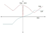
도 2는 본 발명에 따른 벌크 실리콘 멤스의 제조 방법의 패턴된 멤스 본딩 구조물의 전기적 특성 안정화 단계를 거친 경우의 전기적 특성을 나타낸 도면이다.
Claims (5)
- 멤스 구조물을 형성하는 구조물 웨이퍼 및 멤스 구조물을 보호하는 캡 웨이퍼(cap wafer) 간의 금속 본딩 또는 공융 본딩을 통하여 전기적 연결 및 밀봉을 동시에 하는 단계; 및
패턴된 멤스 본딩 구조물의 저항 접촉(ohmic contact)이 균일한 특성을 가지도록, 전기적 특성을 안정화시키기 위한, 패턴된 멤스 본딩 구조물의 전기적 특성 안정화 단계;를 포함하는,
벌크 실리콘 멤스(Bulk Si MEMS)의 제조 방법.
- 제 1 항에 있어서,
상기 패턴된 멤스 본딩 구조물의 전기적 특성 안정화 단계는,
서로 본딩된 상기 구조물 웨이퍼 및 상기 캡 웨이퍼에 대해서, 실온에서 시작하여 상기 구조물 웨이퍼 및 상기 캡 웨이퍼의 본딩 가능 온도보다 낮은 온도인 제 1 온도까지 제 1 시간 동안 승온을 진행하고, 제 2 시간 동안 상기 제 1 온도를 정온으로 유지하고, 제 1 온도에서 시작하여 실온까지 제 1 시간 이상의 제 3 시간 동안 감온을 진행하는 단계를 포함하는,
벌크 실리콘 멤스의 제조 방법.
- 제 2 항에 있어서,
상기 패턴된 멤스 본딩 구조물의 전기적 특성 안정화 단계는,
반도체 공정에서 노출된 금속의 부식을 방지되도록, 대기압보다 낮은 압력 하에서 N2 가스 분위기에서 진행하는 것을 특징으로 하는,
벌크 실리콘 멤스의 제조 방법.
- 제 3 항에 있어서,
상기 금속 본딩은 Au-Au 본딩 또는 Cu-Cu 본딩이고,
상기 공융 본딩은 Au-Sn, Au-Si 본딩, 또는 Al-Ge 본딩인,
벌크 실리콘 멤스의 제조 방법.
- 제 4 항에 있어서,
상기 공융 본딩이 Al-Ge 공융 본딩인 경우,
상기 Al-Ge 공융 본딩은 섭씨 440도~450도에서, 50KN으로 가압하고, 10분간 진행되며,
상기 패턴된 멤스 본딩 구조물의 전기적 특성 안정화 단계는,
서로 본딩된 상기 구조물 웨이퍼 및 상기 캡 웨이퍼에 대해서, 실온에서 시작하여 Al-Ge 공융 반응 온도 이하의 온도인 섭씨 324도 내지 섭씨 420도 범위 내의 온도 중 특정 온도까지 90분 동안 승온을 진행하고, 10분 동안 상기 특정 온도에서 정온으로 유지하고, 상기 특정 온도에서 시작하여 실온까지 90분 이상의 시간 동안 감온을 진행하는 단계를 포함하는,
벌크 실리콘 멤스의 제조 방법.
Priority Applications (2)
| Application Number | Priority Date | Filing Date | Title |
|---|---|---|---|
| KR1020160046967A KR20170119155A (ko) | 2016-04-18 | 2016-04-18 | 벌크 실리콘 멤스의 제조 방법 |
| PCT/KR2016/009952 WO2017183774A1 (ko) | 2016-04-18 | 2016-09-06 | 벌크 실리콘 멤스의 제조 방법 |
Applications Claiming Priority (1)
| Application Number | Priority Date | Filing Date | Title |
|---|---|---|---|
| KR1020160046967A KR20170119155A (ko) | 2016-04-18 | 2016-04-18 | 벌크 실리콘 멤스의 제조 방법 |
Publications (1)
| Publication Number | Publication Date |
|---|---|
| KR20170119155A true KR20170119155A (ko) | 2017-10-26 |
Family
ID=60116834
Family Applications (1)
| Application Number | Title | Priority Date | Filing Date |
|---|---|---|---|
| KR1020160046967A Abandoned KR20170119155A (ko) | 2016-04-18 | 2016-04-18 | 벌크 실리콘 멤스의 제조 방법 |
Country Status (2)
| Country | Link |
|---|---|
| KR (1) | KR20170119155A (ko) |
| WO (1) | WO2017183774A1 (ko) |
Family Cites Families (5)
| Publication number | Priority date | Publication date | Assignee | Title |
|---|---|---|---|---|
| KR970077162A (ko) * | 1996-05-23 | 1997-12-12 | 김주용 | 웨이퍼상의 폴리실리콘층 형성방법 |
| DE102005053722B4 (de) * | 2005-11-10 | 2007-08-16 | Fraunhofer-Gesellschaft zur Förderung der angewandten Forschung e.V. | Deckelwafer, in der Mikrosystemtechnik einsetzbares Bauelement mit einem solchen Wafer sowie Lötverfahren zum Verbinden entsprechender Bauelement-Teile |
| ATE493755T1 (de) * | 2007-05-02 | 2011-01-15 | Siltronic Ag | Siliciumwafer und herstellungsverfahren dafür |
| KR101231412B1 (ko) * | 2009-12-29 | 2013-02-07 | 실트로닉 아게 | 실리콘 웨이퍼 및 그 제조 방법 |
| KR101581542B1 (ko) * | 2014-04-24 | 2015-12-30 | 주식회사 스탠딩에그 | 캡 기판, 구조물 및 그 제조 방법 |
-
2016
- 2016-04-18 KR KR1020160046967A patent/KR20170119155A/ko not_active Abandoned
- 2016-09-06 WO PCT/KR2016/009952 patent/WO2017183774A1/ko not_active Ceased
Also Published As
| Publication number | Publication date |
|---|---|
| WO2017183774A1 (ko) | 2017-10-26 |
Similar Documents
| Publication | Publication Date | Title |
|---|---|---|
| TWI498975B (zh) | 封裝結構與基材的接合方法 | |
| US20110268977A1 (en) | Electronic component device and method for producing the same | |
| CN104112653A (zh) | 一种自补偿背封半导体衬底的制备方法 | |
| RU2008127306A (ru) | Способ изготовления микромеханических устройств, содержащих газопоглотительный материал, и изготовление этим способом устройства | |
| CN105990165A (zh) | 半导体结构及其形成方法 | |
| JP2015220264A (ja) | 半導体装置および半導体装置の製造方法 | |
| US20150224755A1 (en) | Method for coating and bonding substrates | |
| CN108414121B (zh) | 一种GaN压力传感器制备方法及器件 | |
| US20230249961A1 (en) | Semiconductor structure and manufacturing method for the same | |
| JP2016076545A (ja) | 半導体装置 | |
| CN104409375B (zh) | 键合方法和半导体器件的制造方法 | |
| US9824887B2 (en) | Nitride semiconductor device | |
| JPH0787187B2 (ja) | GaAs化合物半導体基板の製造方法 | |
| US20150325538A1 (en) | Semiconductor device and method for producing semiconductor device | |
| JP5432480B2 (ja) | Si基板上のGaN系デバイスの熱処理方法 | |
| KR100942713B1 (ko) | 질화물계 발광소자 및 그 제조방법 | |
| CN103972081B (zh) | 一种内介电层的制备方法 | |
| WO2017183774A1 (ko) | 벌크 실리콘 멤스의 제조 방법 | |
| JP6292104B2 (ja) | 窒化物半導体装置の製造方法 | |
| US20100101840A1 (en) | Application of a self-assembled monolayer as an oxide inhibitor | |
| US11459226B2 (en) | Semiconductor device and semiconductor device manufacturing method | |
| US7566637B2 (en) | Method of inhibition of metal diffusion arising from laser dicing | |
| TWI691034B (zh) | 微電子構件裝置的製造方法及微電子構件裝置 | |
| CN104851792B (zh) | 钝化的处理方法 | |
| TWI559416B (zh) | The fabrication of wafer - level package structure |
Legal Events
| Date | Code | Title | Description |
|---|---|---|---|
| A201 | Request for examination | ||
| PA0109 | Patent application |
St.27 status event code: A-0-1-A10-A12-nap-PA0109 |
|
| PA0201 | Request for examination |
St.27 status event code: A-1-2-D10-D11-exm-PA0201 |
|
| E902 | Notification of reason for refusal | ||
| PE0902 | Notice of grounds for rejection |
St.27 status event code: A-1-2-D10-D21-exm-PE0902 |
|
| AMND | Amendment | ||
| E13-X000 | Pre-grant limitation requested |
St.27 status event code: A-2-3-E10-E13-lim-X000 |
|
| P11-X000 | Amendment of application requested |
St.27 status event code: A-2-2-P10-P11-nap-X000 |
|
| P13-X000 | Application amended |
St.27 status event code: A-2-2-P10-P13-nap-X000 |
|
| E902 | Notification of reason for refusal | ||
| PE0902 | Notice of grounds for rejection |
St.27 status event code: A-1-2-D10-D21-exm-PE0902 |
|
| PG1501 | Laying open of application |
St.27 status event code: A-1-1-Q10-Q12-nap-PG1501 |
|
| T11-X000 | Administrative time limit extension requested |
St.27 status event code: U-3-3-T10-T11-oth-X000 |
|
| AMND | Amendment | ||
| P11-X000 | Amendment of application requested |
St.27 status event code: A-2-2-P10-P11-nap-X000 |
|
| P13-X000 | Application amended |
St.27 status event code: A-2-2-P10-P13-nap-X000 |
|
| E601 | Decision to refuse application | ||
| PE0601 | Decision on rejection of patent |
St.27 status event code: N-2-6-B10-B15-exm-PE0601 |
|
| X091 | Application refused [patent] | ||
| AMND | Amendment | ||
| P11-X000 | Amendment of application requested |
St.27 status event code: A-2-2-P10-P11-nap-X000 |
|
| P13-X000 | Application amended |
St.27 status event code: A-2-2-P10-P13-nap-X000 |
|
| PX0901 | Re-examination |
St.27 status event code: A-2-3-E10-E12-rex-PX0901 |
|
| PX0701 | Decision of registration after re-examination |
St.27 status event code: A-3-4-F10-F13-rex-PX0701 |
|
| X701 | Decision to grant (after re-examination) | ||
| NORF | Unpaid initial registration fee | ||
| PC1904 | Unpaid initial registration fee |
St.27 status event code: A-2-2-U10-U13-oth-PC1904 St.27 status event code: N-2-6-B10-B12-nap-PC1904 |
|
| P22-X000 | Classification modified |
St.27 status event code: A-2-2-P10-P22-nap-X000 |