KR20170120194A - 리소그래피 머신들의 클러스터를 위한 네트워크 아키텍처 및 프로토콜 - Google Patents
리소그래피 머신들의 클러스터를 위한 네트워크 아키텍처 및 프로토콜 Download PDFInfo
- Publication number
- KR20170120194A KR20170120194A KR1020177029925A KR20177029925A KR20170120194A KR 20170120194 A KR20170120194 A KR 20170120194A KR 1020177029925 A KR1020177029925 A KR 1020177029925A KR 20177029925 A KR20177029925 A KR 20177029925A KR 20170120194 A KR20170120194 A KR 20170120194A
- Authority
- KR
- South Korea
- Prior art keywords
- lithography
- data
- subsystems
- subsystem
- control unit
- Prior art date
- Legal status (The legal status is an assumption and is not a legal conclusion. Google has not performed a legal analysis and makes no representation as to the accuracy of the status listed.)
- Granted
Links
Images






Classifications
-
- G—PHYSICS
- G03—PHOTOGRAPHY; CINEMATOGRAPHY; ANALOGOUS TECHNIQUES USING WAVES OTHER THAN OPTICAL WAVES; ELECTROGRAPHY; HOLOGRAPHY
- G03F—PHOTOMECHANICAL PRODUCTION OF TEXTURED OR PATTERNED SURFACES, e.g. FOR PRINTING, FOR PROCESSING OF SEMICONDUCTOR DEVICES; MATERIALS THEREFOR; ORIGINALS THEREFOR; APPARATUS SPECIALLY ADAPTED THEREFOR
- G03F7/00—Photomechanical, e.g. photolithographic, production of textured or patterned surfaces, e.g. printing surfaces; Materials therefor, e.g. comprising photoresists; Apparatus specially adapted therefor
- G03F7/70—Microphotolithographic exposure; Apparatus therefor
- G03F7/70483—Information management; Active and passive control; Testing; Wafer monitoring, e.g. pattern monitoring
- G03F7/70491—Information management, e.g. software; Active and passive control, e.g. details of controlling exposure processes or exposure tool monitoring processes
- G03F7/70508—Data handling in all parts of the microlithographic apparatus, e.g. handling pattern data for addressable masks or data transfer to or from different components within the exposure apparatus
-
- G—PHYSICS
- G06—COMPUTING OR CALCULATING; COUNTING
- G06F—ELECTRIC DIGITAL DATA PROCESSING
- G06F9/00—Arrangements for program control, e.g. control units
- G06F9/06—Arrangements for program control, e.g. control units using stored programs, i.e. using an internal store of processing equipment to receive or retain programs
- G06F9/46—Multiprogramming arrangements
- G06F9/48—Program initiating; Program switching, e.g. by interrupt
-
- B—PERFORMING OPERATIONS; TRANSPORTING
- B82—NANOTECHNOLOGY
- B82Y—SPECIFIC USES OR APPLICATIONS OF NANOSTRUCTURES; MEASUREMENT OR ANALYSIS OF NANOSTRUCTURES; MANUFACTURE OR TREATMENT OF NANOSTRUCTURES
- B82Y10/00—Nanotechnology for information processing, storage or transmission, e.g. quantum computing or single electron logic
-
- B—PERFORMING OPERATIONS; TRANSPORTING
- B82—NANOTECHNOLOGY
- B82Y—SPECIFIC USES OR APPLICATIONS OF NANOSTRUCTURES; MEASUREMENT OR ANALYSIS OF NANOSTRUCTURES; MANUFACTURE OR TREATMENT OF NANOSTRUCTURES
- B82Y40/00—Manufacture or treatment of nanostructures
-
- G—PHYSICS
- G03—PHOTOGRAPHY; CINEMATOGRAPHY; ANALOGOUS TECHNIQUES USING WAVES OTHER THAN OPTICAL WAVES; ELECTROGRAPHY; HOLOGRAPHY
- G03F—PHOTOMECHANICAL PRODUCTION OF TEXTURED OR PATTERNED SURFACES, e.g. FOR PRINTING, FOR PROCESSING OF SEMICONDUCTOR DEVICES; MATERIALS THEREFOR; ORIGINALS THEREFOR; APPARATUS SPECIALLY ADAPTED THEREFOR
- G03F7/00—Photomechanical, e.g. photolithographic, production of textured or patterned surfaces, e.g. printing surfaces; Materials therefor, e.g. comprising photoresists; Apparatus specially adapted therefor
- G03F7/70—Microphotolithographic exposure; Apparatus therefor
- G03F7/70483—Information management; Active and passive control; Testing; Wafer monitoring, e.g. pattern monitoring
-
- G—PHYSICS
- G03—PHOTOGRAPHY; CINEMATOGRAPHY; ANALOGOUS TECHNIQUES USING WAVES OTHER THAN OPTICAL WAVES; ELECTROGRAPHY; HOLOGRAPHY
- G03F—PHOTOMECHANICAL PRODUCTION OF TEXTURED OR PATTERNED SURFACES, e.g. FOR PRINTING, FOR PROCESSING OF SEMICONDUCTOR DEVICES; MATERIALS THEREFOR; ORIGINALS THEREFOR; APPARATUS SPECIALLY ADAPTED THEREFOR
- G03F7/00—Photomechanical, e.g. photolithographic, production of textured or patterned surfaces, e.g. printing surfaces; Materials therefor, e.g. comprising photoresists; Apparatus specially adapted therefor
- G03F7/70—Microphotolithographic exposure; Apparatus therefor
- G03F7/70483—Information management; Active and passive control; Testing; Wafer monitoring, e.g. pattern monitoring
- G03F7/70491—Information management, e.g. software; Active and passive control, e.g. details of controlling exposure processes or exposure tool monitoring processes
- G03F7/70525—Controlling normal operating mode, e.g. matching different apparatus, remote control or prediction of failure
-
- G—PHYSICS
- G03—PHOTOGRAPHY; CINEMATOGRAPHY; ANALOGOUS TECHNIQUES USING WAVES OTHER THAN OPTICAL WAVES; ELECTROGRAPHY; HOLOGRAPHY
- G03F—PHOTOMECHANICAL PRODUCTION OF TEXTURED OR PATTERNED SURFACES, e.g. FOR PRINTING, FOR PROCESSING OF SEMICONDUCTOR DEVICES; MATERIALS THEREFOR; ORIGINALS THEREFOR; APPARATUS SPECIALLY ADAPTED THEREFOR
- G03F7/00—Photomechanical, e.g. photolithographic, production of textured or patterned surfaces, e.g. printing surfaces; Materials therefor, e.g. comprising photoresists; Apparatus specially adapted therefor
- G03F7/70—Microphotolithographic exposure; Apparatus therefor
- G03F7/708—Construction of apparatus, e.g. environment aspects, hygiene aspects or materials
- G03F7/70991—Connection with other apparatus, e.g. multiple exposure stations, particular arrangement of exposure apparatus and pre-exposure and/or post-exposure apparatus; Shared apparatus, e.g. having shared radiation source, shared mask or workpiece stage, shared base-plate; Utilities, e.g. cable, pipe or wireless arrangements for data, power, fluids or vacuum
-
- H—ELECTRICITY
- H01—ELECTRIC ELEMENTS
- H01J—ELECTRIC DISCHARGE TUBES OR DISCHARGE LAMPS
- H01J37/00—Discharge tubes with provision for introducing objects or material to be exposed to the discharge, e.g. for the purpose of examination or processing thereof
- H01J37/30—Electron-beam or ion-beam tubes for localised treatment of objects
- H01J37/317—Electron-beam or ion-beam tubes for localised treatment of objects for changing properties of the objects or for applying thin layers thereon, e.g. for ion implantation
- H01J37/3174—Particle-beam lithography, e.g. electron beam lithography
- H01J37/3177—Multi-beam, e.g. fly's eye, comb probe
-
- H—ELECTRICITY
- H10—SEMICONDUCTOR DEVICES; ELECTRIC SOLID-STATE DEVICES NOT OTHERWISE PROVIDED FOR
- H10W—GENERIC PACKAGES, INTERCONNECTIONS, CONNECTORS OR OTHER CONSTRUCTIONAL DETAILS OF DEVICES COVERED BY CLASS H10
- H10W72/00—Interconnections or connectors in packages
- H10W72/01—Manufacture or treatment
- H10W72/013—Manufacture or treatment of die-attach connectors
- H10W72/01351—Changing the shapes of die-attach connectors
- H10W72/01355—Changing the shapes of die-attach connectors by use of masks
-
- G—PHYSICS
- G05—CONTROLLING; REGULATING
- G05B—CONTROL OR REGULATING SYSTEMS IN GENERAL; FUNCTIONAL ELEMENTS OF SUCH SYSTEMS; MONITORING OR TESTING ARRANGEMENTS FOR SUCH SYSTEMS OR ELEMENTS
- G05B19/00—Program-control systems
- G05B19/02—Program-control systems electric
- G05B19/418—Total factory control, i.e. centrally controlling a plurality of machines, e.g. direct or distributed numerical control [DNC], flexible manufacturing systems [FMS], integrated manufacturing systems [IMS] or computer integrated manufacturing [CIM]
- G05B19/41865—Total factory control, i.e. centrally controlling a plurality of machines, e.g. direct or distributed numerical control [DNC], flexible manufacturing systems [FMS], integrated manufacturing systems [IMS] or computer integrated manufacturing [CIM] characterised by job scheduling, process planning, material flow
-
- G—PHYSICS
- G06—COMPUTING OR CALCULATING; COUNTING
- G06F—ELECTRIC DIGITAL DATA PROCESSING
- G06F9/00—Arrangements for program control, e.g. control units
- G06F9/06—Arrangements for program control, e.g. control units using stored programs, i.e. using an internal store of processing equipment to receive or retain programs
- G06F9/46—Multiprogramming arrangements
- G06F9/48—Program initiating; Program switching, e.g. by interrupt
- G06F9/4806—Task transfer initiation or dispatching
- G06F9/4843—Task transfer initiation or dispatching by program, e.g. task dispatcher, supervisor, operating system
- G06F9/4881—Scheduling strategies for dispatcher, e.g. round robin, multi-level priority queues
-
- H—ELECTRICITY
- H05—ELECTRIC TECHNIQUES NOT OTHERWISE PROVIDED FOR
- H05K—PRINTED CIRCUITS; CASINGS OR CONSTRUCTIONAL DETAILS OF ELECTRIC APPARATUS; MANUFACTURE OF ASSEMBLAGES OF ELECTRICAL COMPONENTS
- H05K2203/00—Indexing scheme relating to apparatus or processes for manufacturing printed circuits covered by H05K3/00
- H05K2203/05—Patterning and lithography; Masks; Details of resist
- H05K2203/0502—Patterning and lithography
-
- Y—GENERAL TAGGING OF NEW TECHNOLOGICAL DEVELOPMENTS; GENERAL TAGGING OF CROSS-SECTIONAL TECHNOLOGIES SPANNING OVER SEVERAL SECTIONS OF THE IPC; TECHNICAL SUBJECTS COVERED BY FORMER USPC CROSS-REFERENCE ART COLLECTIONS [XRACs] AND DIGESTS
- Y10—TECHNICAL SUBJECTS COVERED BY FORMER USPC
- Y10S—TECHNICAL SUBJECTS COVERED BY FORMER USPC CROSS-REFERENCE ART COLLECTIONS [XRACs] AND DIGESTS
- Y10S977/00—Nanotechnology
- Y10S977/84—Manufacture, treatment, or detection of nanostructure
- Y10S977/887—Nanoimprint lithography, i.e. nanostamp
Landscapes
- Engineering & Computer Science (AREA)
- Physics & Mathematics (AREA)
- General Physics & Mathematics (AREA)
- Chemical & Material Sciences (AREA)
- Nanotechnology (AREA)
- Theoretical Computer Science (AREA)
- Crystallography & Structural Chemistry (AREA)
- Manufacturing & Machinery (AREA)
- Software Systems (AREA)
- Epidemiology (AREA)
- Analytical Chemistry (AREA)
- Environmental & Geological Engineering (AREA)
- Computer Networks & Wireless Communication (AREA)
- Public Health (AREA)
- Health & Medical Sciences (AREA)
- Mathematical Physics (AREA)
- Condensed Matter Physics & Semiconductors (AREA)
- General Engineering & Computer Science (AREA)
- Quality & Reliability (AREA)
- Automation & Control Theory (AREA)
- Exposure And Positioning Against Photoresist Photosensitive Materials (AREA)
- Exposure Of Semiconductors, Excluding Electron Or Ion Beam Exposure (AREA)
- Electron Beam Exposure (AREA)
- Container, Conveyance, Adherence, Positioning, Of Wafer (AREA)
- General Factory Administration (AREA)
Abstract
Description
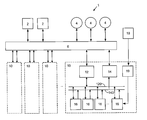
도 2는 리소그래피 엘리먼트들의 클러스터를 포함하는 리소그래피 시스템을 위한 네트워크 아키텍처의 실시예의 개략도이고,
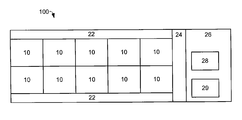
도 3은 리소그래피 엘리먼트들의 클러스터의 레이아웃의 도면이고,
도 4는 하전 입자(charged particle) 리소그래피 엘리먼트의 전자-광학 컬럼(column)의 간략화된 도면이고,
도 5는 본 발명의 실시예에 따른 리소그래피 툴을 위한 OSI 계층화된 모델에서의 엘리먼트 제어 유닛 프로토콜의 개략도이고,
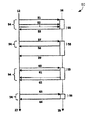
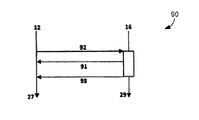
도 6a는 본 발명의 실시예에 따른 접속 시퀀스의 개략도이고,
도 6b는 본 발명의 실시예에 따른 재접속 시퀀스의 개략도이고,
도 6c는 본 발명의 실시예에 따른 실행 명령 시퀀스의 개략도이고,
도 6d는 본 발명의 실시예에 따른 중단(abort) 시퀀스의 개략도이고,
도 6e는 본 발명의 실시예에 따른 경합 조건(race condition)을 갖는 중단 시퀀스의 개략도이고,
도 6f는 본 발명의 실시예에 따른 포괄적인(generic) 명령 동안의 예외 시퀀스의 개략도이고,
도 6g는 본 발명의 실시예에 따른 자발적(spontaneous) 예외의 개략도이고,
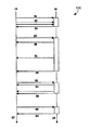
도 6h는 본 발명의 실시예에 따른 실행 명령 동안의 예외의 개략도이다.
Claims (16)
- 하나 이상의 리소그래피 엘리먼트들을 포함하는 리소그래피 시스템 ― 각각의 리소그래피 엘리먼트는 패턴 데이터에 따라 기판들의 독립적 노출을 위해 배열되고, 각각의 리소그래피 엘리먼트는 복수의 리소그래피 서브시스템들을 포함함 ― 에 있어서,
상기 리소그래피 시스템은,
제어 정보의 통신을 위해 상기 복수의 리소그래피 서브시스템들과 적어도 하나의 엘리먼트 제어유닛 사이에 제어 네트워크 경로를 형성하는 제어 네트워크를 더 포함하고,
상기 리소그래피 시스템은:
하나 이상의 웨이퍼들의 노출을 위해 하나 이상의 상기 리소그래피 서브시스템들의 동작을 제어하기 위해, 제어 정보를 상기 적어도 하나의 엘리먼트 제어 유닛에 발행(issue)하고;
상기 엘리먼트 제어 유닛에 프로세스 프로그램 ― 상기 프로세스 프로그램은 미리규정된 명령들 및 연관된 파라미터들의 세트를 포함하고, 각각의 명령은 하나 이상의 상기 리소그래피 서브시스템들에 의해 수행될 미리규정된 동작 또는 동작들의 시퀀스에 대응하고, 그리고 상기 파라미터들은 상기 동작 또는 동작들의 시퀀스가 수행될 방법을 더 규정함 ― 을 발행하도록 배열되며,
상기 프로세스 프로그램 내 미리규정된 명령들의 세트는 하나 이상의 상기 리소그래피 서브시스템들의 업데이팅 또는 업그레이딩 소프트웨어를 포함하는,
하나 이상의 리소그래피 엘리먼트들을 포함하는 리소그래피 시스템. - 제 1 항에 있어서,
상기 엘리먼트 제어 유닛은, 하나 이상의 상기 리소그래피 서브시스템들에 의한 실행을 위해 대응하는 프로세스 잡(process job)을 발생시키도록 상기 프로세스 프로그램을 스케줄링하기 위해 배열되는,
하나 이상의 리소그래피 엘리먼트들을 포함하는 리소그래피 시스템. - 제 2 항에 있어서,
상기 소프트웨어를 업데이트 또는 업그레이드 하기 위한 리소그래피 서브시스템 내의 소프트웨어의 수정(modification)은, 프로세스 잡을 실행함으로써 수행되는,
하나 이상의 리소그래피 엘리먼트들을 포함하는 리소그래피 시스템. - 제 1 항 내지 제 3 항 중 어느 한 항에 있어서,
복수의 상기 리소그래피 서브시스템들은, 리소그래피 서브시스템 내 소프트웨어의 수정이 중앙 디스크 또는 메모리 내 상기 리소그래피 서브시스템을 위한 부트 이미지를 업데이트함으로써 수행되도록, 상기 중앙 디스크 또는 메모리로부터 부팅(boot)을 하도록 구성되는,
하나 이상의 리소그래피 엘리먼트들을 포함하는 리소그래피 시스템. - 제 1 항 내지 제 3 항 중 어느 한 항에 있어서,
상기 리소그래피 시스템은, 데이터를 수집, 저장 및 관리하기 위한 데이터 네트워크, 및 상기 데이터 네트워크를 통해 상기 복수의 리소그래피 서브시스템들에 연결된 데이터 네트워크 허브를 더 포함하고,
복수의 상기 리소그래피 서브시스템들은, 상기 소프트웨어의 업데이팅 또는 업그레이딩이 상기 데이터 네트워크 허브 상에서 상기 리소그래피 서브시스템을 위한 부트 이미지를 업데이팅 함으로써 수행되도록, 상기 데이터 네트워크 허브로부터 부팅을 하도록 구성되는,
하나 이상의 리소그래피 엘리먼트들을 포함하는 리소그래피 시스템. - 제 1 항 내지 제 3 항 중 어느 한 항에 있어서,
상기 엘리먼트 제어 유닛은, 상기 프로세스 프로그램을 스케줄링 하고, 그리고 상기 리소그래피 서브시스템으로 전송된 선행(preceding) 명령의 실행 상태와 상관없이, 상기 스케줄링에 따라 리소그래피 서브시스템에 상기 프로세스 프로그램의 명령을 전송하도록 배열되는,
하나 이상의 리소그래피 엘리먼트들을 포함하는 리소그래피 시스템. - 제 1 항 내지 제 3 항 중 어느 한 항에 있어서,
상기 리소그래피 시스템을 새로운 기능성으로 확장 또는 업그레이드하는 것은, 하나 이상의 상기 리소그래피 서브시스템들 내 소프트웨어의 수정, 그리고 업데이트된 프로세스 프로그램을 발행함으로써 수행되는,
하나 이상의 리소그래피 엘리먼트들을 포함하는 리소그래피 시스템. - 제 7 항에 있어서,
하나 이상의 상기 리소그래피 서브시스템들은, 상기 하나 이상의 리소그래피 서브시스템들 내 소프트웨어의 수정 이후 상기 엘리먼트 제어 유닛에 실행가능한 명령들의 정보를 전송하도록 구성되는,
하나 이상의 리소그래피 엘리먼트들을 포함하는 리소그래피 시스템. - 제 7 항에 있어서,
상기 리소그래피 시스템의 확장 또는 업그레이드는 상기 엘리먼트 제어 유닛 내 소프트웨어의 수정을 필요로 하지 않는,
하나 이상의 리소그래피 엘리먼트들을 포함하는 리소그래피 시스템. - 제 1 항 내지 제 3 항 중 어느 한 항에 있어서,
데이터를 수집, 저장 및 관리하기 위한 데이터 네트워크 ― 상기 데이터는 복수의 상기 리소그래피 서브시스템들의 셋팅(setting)들을 포함함 ― 를 더 포함하고, 상기 리소그래피 서브시스템들은 상기 데이터 네트워크를 통해 데이터 네트워크 허브에 연결되는,
하나 이상의 리소그래피 엘리먼트들을 포함하는 리소그래피 시스템. - 제 10 항에 있어서,
상기 제어 네트워크 및 데이터 네트워크는 별개의 네트워크들을 형성하는,
하나 이상의 리소그래피 엘리먼트들을 포함하는 리소그래피 시스템. - 제 10 항에 있어서,
상기 데이터 네트워크 허브에 의해 저장된 상기 데이터는 타임스탬프(timestamp)로 태깅(tag)되는,
하나 이상의 리소그래피 엘리먼트들을 포함하는 리소그래피 시스템. - 제 10 항에 있어서,
상기 패턴 데이터를 생성하기 위한 페턴 데이터 프로세싱 시스템을 더 포함하고, 상기 패턴 데이터 프로세싱 시스템은 상기 패턴 데이터를 데이터 경로를 통해 하나 이상의 상기 리소그래피 서브시스템들로 전송하도록 배열되며, 상기 데이터 경로는 상기 제어 네트워크 및 데이터 네트워크와 구별되는,
하나 이상의 리소그래피 엘리먼트들을 포함하는 리소그래피 시스템. - 제 1 항 내지 제 3 항 중 어느 한 항에 있어서,
상기 엘리먼트 제어 유닛은 반복된 명령들의 시퀀스를 상기 리소그래피 서브시스템에 전송하도록 구성되고, 상기 리소그래피 서브시스템은 상기 시퀀스 내 명령이 시간 기간 내 실행되지 않은 경우 상기 시퀀스 내 명령을 폐기(discard)하도록 구성되는,
하나 이상의 리소그래피 엘리먼트들을 포함하는 리소그래피 시스템. - 제 1 항 내지 제 3 항 중 어느 한 항에 있어서,
상기 프로세스 프로그램은 대응되는 제 1 명령에 대한 제 1 미리결정된 시간 기간을 규정하고, 상기 엘리먼트 제어 유닛은, 상기 시간 기간의 만료까지 그리고 상기 제 1 명령의 실행 상태와 상관없이, 상기 제 1 명령을 뒤따르는 다음 명령을 개시하는 것을 지연시키도록 배열되는,
하나 이상의 리소그래피 엘리먼트들을 포함하는 리소그래피 시스템. - 제 1 항 내지 제 3 항 중 어느 한 항에 있어서,
상기 제어 네트워크는 실시간 통신 프로토콜을 사용하지 않고 준(quasi) 실시간 수행을 제공하는,
하나 이상의 리소그래피 엘리먼트들을 포함하는 리소그래피 시스템.
Applications Claiming Priority (5)
| Application Number | Priority Date | Filing Date | Title |
|---|---|---|---|
| US201161478117P | 2011-04-22 | 2011-04-22 | |
| US61/478,117 | 2011-04-22 | ||
| US201161533673P | 2011-09-12 | 2011-09-12 | |
| US61/533,673 | 2011-09-12 | ||
| PCT/EP2012/057366 WO2012143548A2 (en) | 2011-04-22 | 2012-04-23 | Network architecture and protocol for cluster of lithography machines |
Related Parent Applications (1)
| Application Number | Title | Priority Date | Filing Date |
|---|---|---|---|
| KR1020137030924A Division KR101791252B1 (ko) | 2011-04-22 | 2012-04-23 | 리소그래피 머신들의 클러스터를 위한 네트워크 아키텍처 및 프로토콜 |
Publications (2)
| Publication Number | Publication Date |
|---|---|
| KR20170120194A true KR20170120194A (ko) | 2017-10-30 |
| KR102072200B1 KR102072200B1 (ko) | 2020-01-31 |
Family
ID=45998374
Family Applications (2)
| Application Number | Title | Priority Date | Filing Date |
|---|---|---|---|
| KR1020177029925A Active KR102072200B1 (ko) | 2011-04-22 | 2012-04-23 | 리소그래피 머신들의 클러스터를 위한 네트워크 아키텍처 및 프로토콜 |
| KR1020137030924A Active KR101791252B1 (ko) | 2011-04-22 | 2012-04-23 | 리소그래피 머신들의 클러스터를 위한 네트워크 아키텍처 및 프로토콜 |
Family Applications After (1)
| Application Number | Title | Priority Date | Filing Date |
|---|---|---|---|
| KR1020137030924A Active KR101791252B1 (ko) | 2011-04-22 | 2012-04-23 | 리소그래피 머신들의 클러스터를 위한 네트워크 아키텍처 및 프로토콜 |
Country Status (8)
| Country | Link |
|---|---|
| US (3) | US9244726B2 (ko) |
| EP (2) | EP2700081B1 (ko) |
| JP (3) | JP5951753B2 (ko) |
| KR (2) | KR102072200B1 (ko) |
| CN (2) | CN103649836B (ko) |
| RU (1) | RU2573398C2 (ko) |
| TW (2) | TWI576670B (ko) |
| WO (2) | WO2012143548A2 (ko) |
Families Citing this family (18)
| Publication number | Priority date | Publication date | Assignee | Title |
|---|---|---|---|---|
| RU2579533C2 (ru) * | 2010-12-14 | 2016-04-10 | МЭППЕР ЛИТОГРАФИ АйПи Б. В. | Литографическая система и способ обработки подложек в такой литографической системе |
| US8893059B2 (en) | 2012-02-06 | 2014-11-18 | Kla-Tencor Corporation | Pattern data system for high-performance maskless electron beam lithography |
| JP2014204012A (ja) * | 2013-04-05 | 2014-10-27 | キヤノン株式会社 | 描画装置、及び物品の製造方法 |
| CN103389625A (zh) * | 2013-07-11 | 2013-11-13 | 浙江大学 | 一种应用于浸没式光刻机中浸液液体传送系统的通讯方法 |
| JP6312379B2 (ja) | 2013-07-19 | 2018-04-18 | キヤノン株式会社 | リソグラフィ装置、リソグラフィ方法、リソグラフィシステム、プログラム、物品の製造方法 |
| JP2015204401A (ja) * | 2014-04-15 | 2015-11-16 | キヤノン株式会社 | リソグラフィ装置、および物品の製造方法 |
| US9927725B2 (en) | 2015-02-16 | 2018-03-27 | Canon Kabushiki Kaisha | Lithography apparatus, lithography method, program, lithography system, and article manufacturing method |
| JP6198805B2 (ja) * | 2015-02-16 | 2017-09-20 | キヤノン株式会社 | リソグラフィ装置、リソグラフィ方法、プログラム、リソグラフィシステムおよび物品製造方法 |
| KR102185748B1 (ko) * | 2016-07-19 | 2020-12-03 | 에이에스엠엘 네델란즈 비.브이. | 직접 기록 마스크리스 리소그래피용 장치 |
| NL2019502B1 (en) | 2016-09-08 | 2018-08-31 | Mapper Lithography Ip Bv | Method and system for fabricating unique chips using a charged particle multi-beamlet lithography system |
| US10714427B2 (en) | 2016-09-08 | 2020-07-14 | Asml Netherlands B.V. | Secure chips with serial numbers |
| US20180068047A1 (en) * | 2016-09-08 | 2018-03-08 | Mapper Lithography Ip B.V. | Method and system for fabricating unique chips using a charged particle multi-beamlet lithography system |
| US10418324B2 (en) | 2016-10-27 | 2019-09-17 | Asml Netherlands B.V. | Fabricating unique chips using a charged particle multi-beamlet lithography system |
| CN106647181B (zh) * | 2016-12-19 | 2018-03-09 | 电子科技大学 | 一种用于dmd无掩膜光刻机的高速图像曝光方法 |
| EP3514640B1 (de) | 2018-01-18 | 2023-05-17 | Gebr. Saacke GmbH & Co.KG | Vorrichtung und verfahren zur bereitstellung von maschinendaten |
| EP4206831A1 (de) * | 2021-12-29 | 2023-07-05 | Siemens Aktiengesellschaft | Verfahren und system zur bereitstellung von zeitkritischen steuerungsanwendungen |
| CN115297183B (zh) * | 2022-07-29 | 2023-11-03 | 天翼云科技有限公司 | 一种数据处理方法、装置、电子设备和存储介质 |
| WO2026074934A1 (ja) * | 2024-10-03 | 2026-04-09 | 東京エレクトロン株式会社 | 基板処理装置及び基板処理装置の検査方法 |
Citations (2)
| Publication number | Priority date | Publication date | Assignee | Title |
|---|---|---|---|---|
| US20070203873A1 (en) * | 2006-02-14 | 2007-08-30 | Asml Netherlands B.V. | Software upgrades in a lithographic apparatus |
| KR20080103570A (ko) * | 2006-02-17 | 2008-11-27 | 가부시키가이샤 니콘 | 조정 방법, 기판 처리 방법, 기판 처리 장치, 노광 장치, 검사 장치, 측정 검사 시스템, 처리 장치, 컴퓨터 시스템, 프로그램 및 정보 기록 매체 |
Family Cites Families (62)
| Publication number | Priority date | Publication date | Assignee | Title |
|---|---|---|---|---|
| US3157308A (en) | 1961-09-05 | 1964-11-17 | Clark Mfg Co J L | Canister type container and method of making the same |
| US3159408A (en) | 1961-10-05 | 1964-12-01 | Grace W R & Co | Chuck |
| US4524308A (en) | 1984-06-01 | 1985-06-18 | Sony Corporation | Circuits for accomplishing electron beam convergence in color cathode ray tubes |
| JP3336436B2 (ja) * | 1991-04-02 | 2002-10-21 | 株式会社ニコン | リソグラフィシステム、情報収集装置、露光装置、及び半導体デバイス製造方法 |
| WO1994025880A1 (en) | 1993-04-30 | 1994-11-10 | Board Of Regents, The University Of Texas System | Megavoltage scanning imager and method for its use |
| TW276353B (ko) | 1993-07-15 | 1996-05-21 | Hitachi Seisakusyo Kk | |
| EP0766405A1 (en) | 1995-09-29 | 1997-04-02 | STMicroelectronics S.r.l. | Successive approximation register without redundancy |
| US5778386A (en) | 1996-05-28 | 1998-07-07 | Taiwan Semiconductor Manufacturing Company Ltd. | Global view storage management system for semiconductor manufacturing plants |
| JP3087696B2 (ja) * | 1997-07-25 | 2000-09-11 | 日本電気株式会社 | 分散メモリ型マルチプロセッサ・システム制御方法およびコンピュータ読み取り可能な記録媒体 |
| KR19990062942A (ko) * | 1997-12-10 | 1999-07-26 | 히로시 오우라 | 전하 입자 빔 노출 장치 |
| US6011952A (en) * | 1998-01-20 | 2000-01-04 | Viasat, Inc. | Self-interference cancellation for relayed communication networks |
| US6610150B1 (en) | 1999-04-02 | 2003-08-26 | Asml Us, Inc. | Semiconductor wafer processing system with vertically-stacked process chambers and single-axis dual-wafer transfer system |
| AU2001238036A1 (en) * | 2000-02-16 | 2001-08-27 | Cymer, Inc. | Process monitoring system for lithography lasers |
| US6714830B2 (en) * | 2000-02-28 | 2004-03-30 | Canon Kabushiki Kaisha | Push-type scheduling for semiconductor fabrication |
| WO2001084382A1 (en) * | 2000-05-04 | 2001-11-08 | Kla-Tencor, Inc. | Methods and systems for lithography process control |
| US7149792B1 (en) * | 2000-11-20 | 2006-12-12 | Axeda Corporation | Device registration mechanism |
| JP2002252161A (ja) | 2001-02-23 | 2002-09-06 | Hitachi Ltd | 半導体製造システム |
| JP4713773B2 (ja) * | 2001-07-09 | 2011-06-29 | 株式会社アドバンテスト | 電子ビーム露光装置及び電子ビーム露光方法 |
| US7280883B2 (en) * | 2001-09-06 | 2007-10-09 | Dainippon Screen Mfg. Co., Ltd. | Substrate processing system managing apparatus information of substrate processing apparatus |
| JP2003288496A (ja) | 2002-03-27 | 2003-10-10 | Toshiba Corp | 描画支援システム、描画支援方法、マスク製造支援システム、及びマスク製造支援方法 |
| JP4078150B2 (ja) | 2002-08-22 | 2008-04-23 | 株式会社日立ハイテクノロジーズ | 半導体製造装置 |
| KR100523839B1 (ko) * | 2002-10-07 | 2005-10-27 | 한국전자통신연구원 | 건식 리소그라피 방법 및 이를 이용한 게이트 패턴 형성방법 |
| EP2302459A3 (en) | 2002-10-25 | 2011-04-06 | Mapper Lithography Ip B.V. | Lithography system |
| CN101414129B (zh) | 2002-10-30 | 2012-11-28 | 迈普尔平版印刷Ip有限公司 | 电子束曝光系统 |
| JP4484868B2 (ja) | 2003-03-10 | 2010-06-16 | マッパー・リソグラフィー・アイピー・ビー.ブイ. | 複数の小ビームを発生させるための装置 |
| KR101168200B1 (ko) | 2003-05-28 | 2012-07-25 | 마퍼 리쏘그라피 아이피 비.브이. | 대전 입자 빔렛 노광 시스템 |
| WO2005010618A2 (en) | 2003-07-30 | 2005-02-03 | Mapper Lithography Ip B.V. | Modulator circuitry |
| US7094613B2 (en) | 2003-10-21 | 2006-08-22 | Applied Materials, Inc. | Method for controlling accuracy and repeatability of an etch process |
| JP2005174959A (ja) * | 2003-12-05 | 2005-06-30 | Nikon Corp | リソグラフィシステム、プログラム及び情報記録媒体、支援装置、並びに露光方法 |
| US7728880B2 (en) * | 2004-06-25 | 2010-06-01 | Qualcomm Incorporated | Automatic white balance method and apparatus |
| JP2006113705A (ja) * | 2004-10-13 | 2006-04-27 | Nikon Corp | 情報処理システム及びプログラム |
| DE102004055149B4 (de) * | 2004-11-16 | 2007-07-19 | Leica Microsystems Lithography Gmbh | Vorrichtung und Verfahren zum Abbilden eines Mehrfach-Partikelstrahls auf ein Substrat |
| CN100361113C (zh) * | 2005-02-05 | 2008-01-09 | 上海微电子装备有限公司 | 步进扫描投影光刻机的高速同步广播总线系统 |
| JP2006338232A (ja) * | 2005-06-01 | 2006-12-14 | Murata Mach Ltd | 通信システム |
| US20070010905A1 (en) | 2005-07-07 | 2007-01-11 | Taiwan Semiconductor Manufacturing Co., Ltd. | Systems and methods for monitoring processing tool |
| US7709815B2 (en) | 2005-09-16 | 2010-05-04 | Mapper Lithography Ip B.V. | Lithography system and projection method |
| US8055727B2 (en) * | 2005-09-22 | 2011-11-08 | Fisher-Rosemount Systems, Inc. | Use of a really simple syndication communication format in a process control system |
| US8090875B2 (en) * | 2005-10-28 | 2012-01-03 | Nikon Corporation | Device and method for connecting device manufacturing processing apparatuses, program, device manufacturing processing system, exposure apparatus and method, and measurement and inspection apparatus and method |
| JP5061904B2 (ja) * | 2005-10-28 | 2012-10-31 | 株式会社ニコン | デバイス製造処理装置間の接続装置及び接続方法、プログラム、デバイス製造処理システム、露光装置及び露光方法、並びに測定検査装置及び測定検査方法 |
| US8134681B2 (en) * | 2006-02-17 | 2012-03-13 | Nikon Corporation | Adjustment method, substrate processing method, substrate processing apparatus, exposure apparatus, inspection apparatus, measurement and/or inspection system, processing apparatus, computer system, program and information recording medium |
| JP4682107B2 (ja) * | 2006-08-28 | 2011-05-11 | 株式会社リコー | 画像形成装置、情報処理方法及び情報処理プログラム |
| US7801635B2 (en) * | 2007-01-30 | 2010-09-21 | Tokyo Electron Limited | Real-time parameter tuning for etch processes |
| US8636458B2 (en) * | 2007-06-06 | 2014-01-28 | Asml Netherlands B.V. | Integrated post-exposure bake track |
| JP4992750B2 (ja) * | 2008-02-14 | 2012-08-08 | 日本電気株式会社 | 中継装置 |
| EP2260499B1 (en) | 2008-02-26 | 2016-11-30 | Mapper Lithography IP B.V. | Projection lens arrangement |
| KR101481950B1 (ko) | 2008-02-26 | 2015-01-14 | 마퍼 리쏘그라피 아이피 비.브이. | 투사 렌즈 배열체 |
| US8445869B2 (en) | 2008-04-15 | 2013-05-21 | Mapper Lithography Ip B.V. | Projection lens arrangement |
| US8258484B2 (en) | 2008-04-15 | 2012-09-04 | Mapper Lithography Ip B.V. | Beamlet blanker arrangement |
| US8502176B2 (en) | 2008-05-23 | 2013-08-06 | Mapper Lithography Ip B.V. | Imaging system |
| WO2009147202A1 (en) | 2008-06-04 | 2009-12-10 | Mapper Lithography Ip B.V. | Writing strategy |
| JP2010067759A (ja) * | 2008-09-10 | 2010-03-25 | Canon Inc | 露光装置 |
| EP2406810B1 (en) | 2008-10-01 | 2014-09-17 | Mapper Lithography IP B.V. | Electrostatic lens structure |
| JP2010093125A (ja) * | 2008-10-09 | 2010-04-22 | Toray Eng Co Ltd | 基板処理システムおよび基板処理方法 |
| JP5008768B2 (ja) * | 2008-12-15 | 2012-08-22 | 東京エレクトロン株式会社 | 基板処理システム、基板処理方法、プログラムを記憶した記憶媒体およびバルブ |
| JP4615071B2 (ja) | 2008-12-29 | 2011-01-19 | キヤノンアネルバ株式会社 | 基板処理システム及び基板処理装置 |
| NL2004392A (en) * | 2009-04-15 | 2010-10-18 | Asml Netherlands Bv | Lithographic apparatus, control system, multi-core processor, and a method to start tasks on a multi-core processor. |
| EP3144955A1 (en) | 2009-05-20 | 2017-03-22 | Mapper Lithography IP B.V. | Method for exposing a wafer |
| CN102460633B (zh) * | 2009-05-20 | 2014-12-17 | 迈普尔平版印刷Ip有限公司 | 用于光刻系统的图案数据转换器 |
| JP2011054679A (ja) * | 2009-08-31 | 2011-03-17 | Hitachi Kokusai Electric Inc | 基板処理装置 |
| JP5392190B2 (ja) | 2010-06-01 | 2014-01-22 | 東京エレクトロン株式会社 | 基板処理システム及び基板処理方法 |
| US8822106B2 (en) * | 2012-04-13 | 2014-09-02 | Taiwan Semiconductor Manufacturing Company, Ltd. | Grid refinement method |
| CN107407595B (zh) | 2015-04-03 | 2018-09-07 | 株式会社日立高新技术 | 光量检测装置、利用其的免疫分析装置及电荷粒子束装置 |
-
2012
- 2012-04-23 KR KR1020177029925A patent/KR102072200B1/ko active Active
- 2012-04-23 EP EP12719948.7A patent/EP2700081B1/en active Active
- 2012-04-23 US US13/453,008 patent/US9244726B2/en active Active
- 2012-04-23 RU RU2013151876/07A patent/RU2573398C2/ru active
- 2012-04-23 WO PCT/EP2012/057366 patent/WO2012143548A2/en not_active Ceased
- 2012-04-23 JP JP2014505664A patent/JP5951753B2/ja active Active
- 2012-04-23 WO PCT/EP2012/057385 patent/WO2012143555A2/en not_active Ceased
- 2012-04-23 JP JP2014505667A patent/JP6042410B2/ja active Active
- 2012-04-23 TW TW101114468A patent/TWI576670B/zh active
- 2012-04-23 KR KR1020137030924A patent/KR101791252B1/ko active Active
- 2012-04-23 CN CN201280030773.3A patent/CN103649836B/zh active Active
- 2012-04-23 EP EP12716017.4A patent/EP2699966B1/en active Active
- 2012-04-23 TW TW101114467A patent/TWI526789B/zh active
- 2012-04-23 US US13/452,990 patent/US9086912B2/en active Active
- 2012-04-23 CN CN201610308354.1A patent/CN105974743B/zh active Active
-
2015
- 2015-06-15 US US14/738,962 patent/US9507629B2/en active Active
-
2016
- 2016-05-23 JP JP2016102480A patent/JP6550623B2/ja active Active
Patent Citations (2)
| Publication number | Priority date | Publication date | Assignee | Title |
|---|---|---|---|---|
| US20070203873A1 (en) * | 2006-02-14 | 2007-08-30 | Asml Netherlands B.V. | Software upgrades in a lithographic apparatus |
| KR20080103570A (ko) * | 2006-02-17 | 2008-11-27 | 가부시키가이샤 니콘 | 조정 방법, 기판 처리 방법, 기판 처리 장치, 노광 장치, 검사 장치, 측정 검사 시스템, 처리 장치, 컴퓨터 시스템, 프로그램 및 정보 기록 매체 |
Also Published As
Similar Documents
| Publication | Publication Date | Title |
|---|---|---|
| KR101791252B1 (ko) | 리소그래피 머신들의 클러스터를 위한 네트워크 아키텍처 및 프로토콜 | |
| CN111638970B (zh) | 以网络为中心的进程控制系统中的冗余 | |
| CN101213552B (zh) | 带有统计可重复的响应时间的多功能半导体制造控制器 | |
| TWI517202B (zh) | 處方及元件控制模組及其方法 | |
| US6480854B1 (en) | Method and apparatus for increasing database availability | |
| US20130016327A1 (en) | Lithography system and method for storing positional data of a target | |
| JP5523005B2 (ja) | 情報処理方法、及び情報処理装置 | |
| JP7336207B2 (ja) | 基板処理システム、基板処理システムの制御方法、プログラム、および物品製造方法 | |
| EP4243350A1 (en) | Control device, system, lithography device, article manufacturing method, control method, and program | |
| KR102964195B1 (ko) | 제어장치, 시스템, 리소그래피 장치, 물품의 제조방법, 제어방법 및 프로그램 | |
| EP4621572A1 (en) | Orchestration device for a distributed processing system | |
| JP3327234B2 (ja) | デバイス製造支援装置、デバイス製造システム、及びデバイス製造方法 | |
| CN117789957A (zh) | 用于手术机器人的数据交互系统、方法、装置及存储介质 |
Legal Events
| Date | Code | Title | Description |
|---|---|---|---|
| A107 | Divisional application of patent | ||
| PA0104 | Divisional application for international application |
St.27 status event code: A-0-1-A10-A18-div-PA0104 St.27 status event code: A-0-1-A10-A16-div-PA0104 |
|
| PG1501 | Laying open of application |
St.27 status event code: A-1-1-Q10-Q12-nap-PG1501 |
|
| A201 | Request for examination | ||
| AMND | Amendment | ||
| P11-X000 | Amendment of application requested |
St.27 status event code: A-2-2-P10-P11-nap-X000 |
|
| P13-X000 | Application amended |
St.27 status event code: A-2-2-P10-P13-nap-X000 |
|
| PA0201 | Request for examination |
St.27 status event code: A-1-2-D10-D11-exm-PA0201 |
|
| E902 | Notification of reason for refusal | ||
| PE0902 | Notice of grounds for rejection |
St.27 status event code: A-1-2-D10-D21-exm-PE0902 |
|
| T11-X000 | Administrative time limit extension requested |
St.27 status event code: U-3-3-T10-T11-oth-X000 |
|
| T11-X000 | Administrative time limit extension requested |
St.27 status event code: U-3-3-T10-T11-oth-X000 |
|
| T11-X000 | Administrative time limit extension requested |
St.27 status event code: U-3-3-T10-T11-oth-X000 |
|
| T11-X000 | Administrative time limit extension requested |
St.27 status event code: U-3-3-T10-T11-oth-X000 |
|
| AMND | Amendment | ||
| P11-X000 | Amendment of application requested |
St.27 status event code: A-2-2-P10-P11-nap-X000 |
|
| P13-X000 | Application amended |
St.27 status event code: A-2-2-P10-P13-nap-X000 |
|
| R17-X000 | Change to representative recorded |
St.27 status event code: A-3-3-R10-R17-oth-X000 |
|
| E601 | Decision to refuse application | ||
| PE0601 | Decision on rejection of patent |
St.27 status event code: N-2-6-B10-B15-exm-PE0601 |
|
| X091 | Application refused [patent] | ||
| T11-X000 | Administrative time limit extension requested |
St.27 status event code: U-3-3-T10-T11-oth-X000 |
|
| T13-X000 | Administrative time limit extension granted |
St.27 status event code: U-3-3-T10-T13-oth-X000 |
|
| T11-X000 | Administrative time limit extension requested |
St.27 status event code: U-3-3-T10-T11-oth-X000 |
|
| N231 | Notification of change of applicant | ||
| PN2301 | Change of applicant |
St.27 status event code: A-3-3-R10-R13-asn-PN2301 St.27 status event code: A-3-3-R10-R11-asn-PN2301 |
|
| T13-X000 | Administrative time limit extension granted |
St.27 status event code: U-3-3-T10-T13-oth-X000 |
|
| AMND | Amendment | ||
| P11-X000 | Amendment of application requested |
St.27 status event code: A-2-2-P10-P11-nap-X000 |
|
| P13-X000 | Application amended |
St.27 status event code: A-2-2-P10-P13-nap-X000 |
|
| PX0901 | Re-examination |
St.27 status event code: A-2-3-E10-E12-rex-PX0901 |
|
| PX0701 | Decision of registration after re-examination |
St.27 status event code: A-3-4-F10-F13-rex-PX0701 |
|
| X701 | Decision to grant (after re-examination) | ||
| GRNT | Written decision to grant | ||
| PR0701 | Registration of establishment |
St.27 status event code: A-2-4-F10-F11-exm-PR0701 |
|
| PR1002 | Payment of registration fee |
St.27 status event code: A-2-2-U10-U12-oth-PR1002 Fee payment year number: 1 |
|
| PG1601 | Publication of registration |
St.27 status event code: A-4-4-Q10-Q13-nap-PG1601 |
|
| PR1001 | Payment of annual fee |
St.27 status event code: A-4-4-U10-U11-oth-PR1001 Fee payment year number: 4 |
|
| PR1001 | Payment of annual fee |
St.27 status event code: A-4-4-U10-U11-oth-PR1001 Fee payment year number: 5 |
|
| P22-X000 | Classification modified |
St.27 status event code: A-4-4-P10-P22-nap-X000 |
|
| PR1001 | Payment of annual fee |
St.27 status event code: A-4-4-U10-U11-oth-PR1001 Fee payment year number: 6 |
|
| U11 | Full renewal or maintenance fee paid |
Free format text: ST27 STATUS EVENT CODE: A-4-4-U10-U11-OTH-PR1001 (AS PROVIDED BY THE NATIONAL OFFICE) Year of fee payment: 6 |
|
| P22-X000 | Classification modified |
St.27 status event code: A-4-4-P10-P22-nap-X000 |