KR20200051456A - 차량 전장용 디바이스 - Google Patents
차량 전장용 디바이스 Download PDFInfo
- Publication number
- KR20200051456A KR20200051456A KR1020190068581A KR20190068581A KR20200051456A KR 20200051456 A KR20200051456 A KR 20200051456A KR 1020190068581 A KR1020190068581 A KR 1020190068581A KR 20190068581 A KR20190068581 A KR 20190068581A KR 20200051456 A KR20200051456 A KR 20200051456A
- Authority
- KR
- South Korea
- Prior art keywords
- film
- printing
- touch
- vehicle
- pct
- Prior art date
- Legal status (The legal status is an assumption and is not a legal conclusion. Google has not performed a legal analysis and makes no representation as to the accuracy of the status listed.)
- Ceased
Links
Images




Classifications
-
- H—ELECTRICITY
- H05—ELECTRIC TECHNIQUES NOT OTHERWISE PROVIDED FOR
- H05K—PRINTED CIRCUITS; CASINGS OR CONSTRUCTIONAL DETAILS OF ELECTRIC APPARATUS; MANUFACTURE OF ASSEMBLAGES OF ELECTRICAL COMPONENTS
- H05K3/00—Apparatus or processes for manufacturing printed circuits
- H05K3/10—Apparatus or processes for manufacturing printed circuits in which conductive material is applied to the insulating support in such a manner as to form the desired conductive pattern
- H05K3/12—Apparatus or processes for manufacturing printed circuits in which conductive material is applied to the insulating support in such a manner as to form the desired conductive pattern using thick film techniques, e.g. printing techniques to apply the conductive material or similar techniques for applying conductive paste or ink patterns
-
- G—PHYSICS
- G06—COMPUTING OR CALCULATING; COUNTING
- G06F—ELECTRIC DIGITAL DATA PROCESSING
- G06F3/00—Input arrangements for transferring data to be processed into a form capable of being handled by the computer; Output arrangements for transferring data from processing unit to output unit, e.g. interface arrangements
- G06F3/01—Input arrangements or combined input and output arrangements for interaction between user and computer
- G06F3/03—Arrangements for converting the position or the displacement of a member into a coded form
- G06F3/041—Digitisers, e.g. for touch screens or touch pads, characterised by the transducing means
-
- H—ELECTRICITY
- H05—ELECTRIC TECHNIQUES NOT OTHERWISE PROVIDED FOR
- H05K—PRINTED CIRCUITS; CASINGS OR CONSTRUCTIONAL DETAILS OF ELECTRIC APPARATUS; MANUFACTURE OF ASSEMBLAGES OF ELECTRICAL COMPONENTS
- H05K3/00—Apparatus or processes for manufacturing printed circuits
- H05K3/22—Secondary treatment of printed circuits
- H05K3/28—Applying non-metallic protective coatings
-
- H—ELECTRICITY
- H05—ELECTRIC TECHNIQUES NOT OTHERWISE PROVIDED FOR
- H05K—PRINTED CIRCUITS; CASINGS OR CONSTRUCTIONAL DETAILS OF ELECTRIC APPARATUS; MANUFACTURE OF ASSEMBLAGES OF ELECTRICAL COMPONENTS
- H05K2201/00—Indexing scheme relating to printed circuits covered by H05K1/00
- H05K2201/01—Dielectrics
- H05K2201/0137—Materials
- H05K2201/0154—Polyimide
-
- H—ELECTRICITY
- H05—ELECTRIC TECHNIQUES NOT OTHERWISE PROVIDED FOR
- H05K—PRINTED CIRCUITS; CASINGS OR CONSTRUCTIONAL DETAILS OF ELECTRIC APPARATUS; MANUFACTURE OF ASSEMBLAGES OF ELECTRICAL COMPONENTS
- H05K2201/00—Indexing scheme relating to printed circuits covered by H05K1/00
- H05K2201/10—Details of components or other objects attached to or integrated in a printed circuit board
- H05K2201/10007—Types of components
- H05K2201/10106—Light emitting diode [LED]
Landscapes
- Engineering & Computer Science (AREA)
- Manufacturing & Machinery (AREA)
- Microelectronics & Electronic Packaging (AREA)
- General Engineering & Computer Science (AREA)
- Theoretical Computer Science (AREA)
- Human Computer Interaction (AREA)
- Physics & Mathematics (AREA)
- General Physics & Mathematics (AREA)
- Structure Of Printed Boards (AREA)
Abstract
Description
도 8은 필름 기재상에 형성되는 인쇄방식의 패터닝 형성방법을 이용하는 전장용 디바이스 제조방법을 나타낸 공정 순서도이다.
도 9는 차량 램프용 LED모듈로 사용하기 위한 차량 전장용 디바이스를 나타낸 예시도이다.
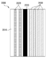
도 10은 차량용 터치모듈로 사용하기 위한 본 발명의 일 실시예에 따른 차량 전장용 디바이스를 나타낸 예시이다.
도 11은 차량용 터치모듈로 사용하기 위한 본 발명의 다른 실시예에 따른 차량 전장용 디바이스를 나타낸 예시도이다.
도 12 내지 도 14는 차량용 FFC형 버스바 케이블로 사용하기 위한 차량 전장용 디바이스를 나타낸 예시도이다.
도 15 내지 도 17은 차량용 후방카메라 FFC형 하이브리드 플랙시블 케이블로 사용하기 위한 차량 전장용 디바이스를 나타낸 예시도이다.
830 : 터치인식부 840 : 터치외곽부
850 : 카본인쇄부 860 : 광학양면테이프
910 : PCT필름 920 : ITO층
930 : 인쇄층 940 : 광학양면테이프
950 : 접착기구물
Claims (4)
- 차량용 터치모듈로 사용하기 위한 차량 전장용 디바이스에 있어서,
커넥터연결부를 갖는 인쇄방식 터치필름;
상기 인쇄방식 터치필름의 상부 또는 하부의 일면에 구비되는 PCT필름;
상기 PCT필름 상에 형성되고, 잉크젯, 스크린프린팅, 그라비아 인쇄방식 중에서 선택된 어느 1군의 인쇄방식을 통해 금속소재에 의한 메쉬형 패턴으로 형성되는 터치인식부;
상기 터치인식부에 연결되고 터치인식부의 가장 자리에 형성되는 것으로서, 금속 인쇄방식으로 형성되는 터치외곽부;
상기 터치외곽부와 전기적으로 연결되게 형성되는 카본인쇄부; 및
상기 PCT필름의 일면에 구비되는 광학양면테이프;를 포함하며,
상기 광학양면테이프는 사출물에 부착할 수 있도록 오토클레이브나 UV의 공정방법으로 형성된 차량 전장용 디바이스. - 제1항에 있어서,
상기 메쉬형 패턴으로 형성되는 터치인식부는 선폭 40um 이하로 형성시킨 차량 전장용 디바이스. - 제2항에 있어서,
상기 터치인식부의 매쉬형 패턴에 대해 선폭 40um 이하로 형성시키기 위해 오프셋 방식으로 식각 처리하여 형성하는 차량 전장용 디바이스. - 차량용 터치모듈로 사용하기 위한 차량 전장용 디바이스에 있어서,
PCT필름;
상기 PCT필름의 상면에 잉크젯, 스크린프린팅, 그라비아 중에서 선택된 어느 1군의 인쇄방식을 통해 ITO물질로 형성되는 ITO층;
상기 ITO층의 상면에 잉크젯, 스크린프린팅, 그라비아 중에서 선택된 어느 1군의 인쇄방식을 통해 형성되는 인쇄층;
상기 인쇄층의 상면에 부착되는 광학양면테이프; 및
상기 광학양면테이프를 매개로 부착되는 접착기구물;을 포함하는 차량 전장용 디바이스.
Priority Applications (1)
| Application Number | Priority Date | Filing Date | Title |
|---|---|---|---|
| KR1020190068581A KR20200051456A (ko) | 2019-06-11 | 2019-06-11 | 차량 전장용 디바이스 |
Applications Claiming Priority (1)
| Application Number | Priority Date | Filing Date | Title |
|---|---|---|---|
| KR1020190068581A KR20200051456A (ko) | 2019-06-11 | 2019-06-11 | 차량 전장용 디바이스 |
Related Parent Applications (1)
| Application Number | Title | Priority Date | Filing Date |
|---|---|---|---|
| KR1020180133581A Division KR102152101B1 (ko) | 2018-11-02 | 2018-11-02 | 차량 전장용 디바이스 |
Publications (1)
| Publication Number | Publication Date |
|---|---|
| KR20200051456A true KR20200051456A (ko) | 2020-05-13 |
Family
ID=70729946
Family Applications (1)
| Application Number | Title | Priority Date | Filing Date |
|---|---|---|---|
| KR1020190068581A Ceased KR20200051456A (ko) | 2019-06-11 | 2019-06-11 | 차량 전장용 디바이스 |
Country Status (1)
| Country | Link |
|---|---|
| KR (1) | KR20200051456A (ko) |
Citations (2)
| Publication number | Priority date | Publication date | Assignee | Title |
|---|---|---|---|---|
| KR20140096039A (ko) | 2011-10-27 | 2014-08-04 | 후지필름 가부시키가이샤 | 패턴형성방법, 다층 레지스트 패턴, 유기용제 현상용 다층 필름, 전자 디바이스의 제조방법 및 전자 디바이스 |
| KR101501449B1 (ko) | 2014-04-16 | 2015-03-12 | 연세대학교 산학협력단 | 금속 나노 입자의 국소 표면 플라즈몬 공명을 이용한 패터닝 장치 및 이를 이용한 패턴 형성방법 |
-
2019
- 2019-06-11 KR KR1020190068581A patent/KR20200051456A/ko not_active Ceased
Patent Citations (2)
| Publication number | Priority date | Publication date | Assignee | Title |
|---|---|---|---|---|
| KR20140096039A (ko) | 2011-10-27 | 2014-08-04 | 후지필름 가부시키가이샤 | 패턴형성방법, 다층 레지스트 패턴, 유기용제 현상용 다층 필름, 전자 디바이스의 제조방법 및 전자 디바이스 |
| KR101501449B1 (ko) | 2014-04-16 | 2015-03-12 | 연세대학교 산학협력단 | 금속 나노 입자의 국소 표면 플라즈몬 공명을 이용한 패터닝 장치 및 이를 이용한 패턴 형성방법 |
Similar Documents
| Publication | Publication Date | Title |
|---|---|---|
| JP6651212B1 (ja) | 車両用バスバーケーブル | |
| US20200344885A1 (en) | Circuit structure | |
| KR100861123B1 (ko) | 비엘유용 연성 인쇄회로기판 및 비엘유 | |
| KR20200051457A (ko) | 차량 전장용 디바이스 | |
| US10631415B2 (en) | Electronic device and manufacturing method thereof | |
| KR20200051456A (ko) | 차량 전장용 디바이스 | |
| US10797211B2 (en) | Method of manufacturing support structures for lighting devices and corresponding device | |
| KR20200051455A (ko) | 차량 전장용 디바이스 | |
| KR20200051460A (ko) | 필름 기재상에 형성되는 인쇄방식의 패터닝 형성방법 | |
| KR20200051458A (ko) | 전장용 디바이스의 제조방법 | |
| KR20200051459A (ko) | 전장용 디바이스의 제조방법 | |
| CN110876239B (zh) | 电路板及其制作方法 | |
| KR20200135909A (ko) | 차량 전장용 디바이스의 제조방법 | |
| KR20200135755A (ko) | 필름 기재상에 형성되는 인쇄방식의 패터닝 형성방법 | |
| KR20200135754A (ko) | 차량 전장용 디바이스의 제조방법 | |
| KR20200135753A (ko) | 차량 전장용 디바이스 | |
| WO2015003929A1 (en) | Method for manufacturing a printed circuit board assembly based on printed electronics and printed circuit board assembly | |
| US10302282B2 (en) | Support structure for lighting devices, corresponding lighting device and method | |
| US10020250B2 (en) | Interposer, module, and method of producing interposer | |
| KR102749868B1 (ko) | 고방열 유연전극회로 및 칩실장 패키지 구조물과 그 제조 방법 | |
| KR102680894B1 (ko) | 입체가공형 터치패드 및 그 형성방법 | |
| CN108322995A (zh) | 一种电子线路结构 | |
| JP2006040967A (ja) | 多層フレキシブルプリント基板およびこれを用いた圧接接続構造 |
Legal Events
| Date | Code | Title | Description |
|---|---|---|---|
| PA0107 | Divisional application |
Comment text: Divisional Application of Patent Patent event date: 20190611 Patent event code: PA01071R01D Filing date: 20181102 Application number text: 1020180133581 |
|
| PA0201 | Request for examination | ||
| PE0902 | Notice of grounds for rejection |
Comment text: Notification of reason for refusal Patent event date: 20200114 Patent event code: PE09021S01D |
|
| PG1501 | Laying open of application | ||
| E902 | Notification of reason for refusal | ||
| PE0902 | Notice of grounds for rejection |
Comment text: Notification of reason for refusal Patent event date: 20201111 Patent event code: PE09021S01D |
|
| E601 | Decision to refuse application | ||
| PE0601 | Decision on rejection of patent |
Patent event date: 20210824 Comment text: Decision to Refuse Application Patent event code: PE06012S01D Patent event date: 20201111 Comment text: Notification of reason for refusal Patent event code: PE06011S01I Patent event date: 20200114 Comment text: Notification of reason for refusal Patent event code: PE06011S01I |