KR20200051459A - 전장용 디바이스의 제조방법 - Google Patents
전장용 디바이스의 제조방법 Download PDFInfo
- Publication number
- KR20200051459A KR20200051459A KR1020190068584A KR20190068584A KR20200051459A KR 20200051459 A KR20200051459 A KR 20200051459A KR 1020190068584 A KR1020190068584 A KR 1020190068584A KR 20190068584 A KR20190068584 A KR 20190068584A KR 20200051459 A KR20200051459 A KR 20200051459A
- Authority
- KR
- South Korea
- Prior art keywords
- film
- printing
- pct
- layer
- vehicle
- Prior art date
- Legal status (The legal status is an assumption and is not a legal conclusion. Google has not performed a legal analysis and makes no representation as to the accuracy of the status listed.)
- Ceased
Links
Images






Classifications
-
- H—ELECTRICITY
- H05—ELECTRIC TECHNIQUES NOT OTHERWISE PROVIDED FOR
- H05K—PRINTED CIRCUITS; CASINGS OR CONSTRUCTIONAL DETAILS OF ELECTRIC APPARATUS; MANUFACTURE OF ASSEMBLAGES OF ELECTRICAL COMPONENTS
- H05K3/00—Apparatus or processes for manufacturing printed circuits
- H05K3/10—Apparatus or processes for manufacturing printed circuits in which conductive material is applied to the insulating support in such a manner as to form the desired conductive pattern
- H05K3/12—Apparatus or processes for manufacturing printed circuits in which conductive material is applied to the insulating support in such a manner as to form the desired conductive pattern using thick film techniques, e.g. printing techniques to apply the conductive material or similar techniques for applying conductive paste or ink patterns
-
- G—PHYSICS
- G06—COMPUTING OR CALCULATING; COUNTING
- G06F—ELECTRIC DIGITAL DATA PROCESSING
- G06F3/00—Input arrangements for transferring data to be processed into a form capable of being handled by the computer; Output arrangements for transferring data from processing unit to output unit, e.g. interface arrangements
- G06F3/01—Input arrangements or combined input and output arrangements for interaction between user and computer
- G06F3/03—Arrangements for converting the position or the displacement of a member into a coded form
- G06F3/041—Digitisers, e.g. for touch screens or touch pads, characterised by the transducing means
-
- H—ELECTRICITY
- H05—ELECTRIC TECHNIQUES NOT OTHERWISE PROVIDED FOR
- H05K—PRINTED CIRCUITS; CASINGS OR CONSTRUCTIONAL DETAILS OF ELECTRIC APPARATUS; MANUFACTURE OF ASSEMBLAGES OF ELECTRICAL COMPONENTS
- H05K3/00—Apparatus or processes for manufacturing printed circuits
- H05K3/22—Secondary treatment of printed circuits
- H05K3/28—Applying non-metallic protective coatings
-
- H—ELECTRICITY
- H05—ELECTRIC TECHNIQUES NOT OTHERWISE PROVIDED FOR
- H05K—PRINTED CIRCUITS; CASINGS OR CONSTRUCTIONAL DETAILS OF ELECTRIC APPARATUS; MANUFACTURE OF ASSEMBLAGES OF ELECTRICAL COMPONENTS
- H05K2201/00—Indexing scheme relating to printed circuits covered by H05K1/00
- H05K2201/01—Dielectrics
- H05K2201/0137—Materials
- H05K2201/0154—Polyimide
-
- H—ELECTRICITY
- H05—ELECTRIC TECHNIQUES NOT OTHERWISE PROVIDED FOR
- H05K—PRINTED CIRCUITS; CASINGS OR CONSTRUCTIONAL DETAILS OF ELECTRIC APPARATUS; MANUFACTURE OF ASSEMBLAGES OF ELECTRICAL COMPONENTS
- H05K2201/00—Indexing scheme relating to printed circuits covered by H05K1/00
- H05K2201/10—Details of components or other objects attached to or integrated in a printed circuit board
- H05K2201/10007—Types of components
- H05K2201/10106—Light emitting diode [LED]
Landscapes
- Engineering & Computer Science (AREA)
- Manufacturing & Machinery (AREA)
- Microelectronics & Electronic Packaging (AREA)
- General Engineering & Computer Science (AREA)
- Theoretical Computer Science (AREA)
- Human Computer Interaction (AREA)
- Physics & Mathematics (AREA)
- General Physics & Mathematics (AREA)
- Structure Of Printed Boards (AREA)
Abstract
Description
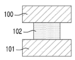
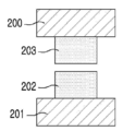
도 7은 본 발명에 따른 전장용 디바이스의 제조방법의 일 실시예를 설명하기 위해 나타낸 개략적 예시도이다.
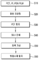
도 8은 본 발명에 따른 전장용 디바이스의 제조방법의 다른 실시예를 나타낸 공정 순서도이다.
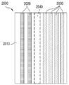
도 9는 차량 램프용 LED모듈로 사용하기 위한 차량 전장용 디바이스를 나타낸 예시도이다.
도 10은 차량용 메탈메쉬형 터치모듈로 사용하기 위한 차량 전장용 디바이스를 나타낸 예시이다.
도 11은 차량용 ITO형 터치모듈로 사용하기 위한 차량 전장용 디바이스를 나타낸 예시도이다.
도 12 내지 도 14는 차량용 FFC형 버스바 케이블로 사용하기 위한 차량 전장용 디바이스를 나타낸 예시도이다.
도 15 내지 도 17은 차량용 후방카메라 FFC형 하이브리드 플랙시블 케이블로 사용하기 위한 차량 전장용 디바이스를 나타낸 예시도이다.
S30 : 커버레이필름 합지단계 S40 : 실크인쇄단계
S50 : 외곽가공단계 S60 : 방열소재 합지단계
Claims (1)
- (A) PI필름, PEN필름, PCT필름 중에서 선택된 어느 1종을 기재필름으로 구비하는 단계;
(B) 상기 기재필름의 상면에 잉크젯, 스크린프린팅, 그라비아 중에서 선택된 어느 1군의 인쇄방식을 통해 금속소재 또는 반도체물질을 인쇄하여 패턴층을 형성하는 단계;
(C) 상기 패턴층을 커버하도록 PCT필름을 커버레이필름으로 구비하여 합지하는 단계;
(D) 상기 커버레이필름으로 합지된 PCT필름의 상면에 실크 인쇄방식에 의한 실크인쇄층을 형성하는 단계;
(E) 상기 (D)단계를 마친 결과물에 대해 금형 또는 레이저가공을 통해 외곽을 가공하여 외형 형상을 형성하는 단계; 및
(F) 상기 (E)단계를 마친 결과물의 하부에 방열기능을 위한 알루미늄플레이트를 합지하는 단계;를 포함하는 전장용 디바이스의 제조방법.
Priority Applications (1)
| Application Number | Priority Date | Filing Date | Title |
|---|---|---|---|
| KR1020190068584A KR20200051459A (ko) | 2019-06-11 | 2019-06-11 | 전장용 디바이스의 제조방법 |
Applications Claiming Priority (1)
| Application Number | Priority Date | Filing Date | Title |
|---|---|---|---|
| KR1020190068584A KR20200051459A (ko) | 2019-06-11 | 2019-06-11 | 전장용 디바이스의 제조방법 |
Related Parent Applications (1)
| Application Number | Title | Priority Date | Filing Date |
|---|---|---|---|
| KR1020180133581A Division KR102152101B1 (ko) | 2018-11-02 | 2018-11-02 | 차량 전장용 디바이스 |
Related Child Applications (1)
| Application Number | Title | Priority Date | Filing Date |
|---|---|---|---|
| KR1020200157632A Division KR20200135754A (ko) | 2020-11-23 | 2020-11-23 | 차량 전장용 디바이스의 제조방법 |
Publications (1)
| Publication Number | Publication Date |
|---|---|
| KR20200051459A true KR20200051459A (ko) | 2020-05-13 |
Family
ID=70729953
Family Applications (1)
| Application Number | Title | Priority Date | Filing Date |
|---|---|---|---|
| KR1020190068584A Ceased KR20200051459A (ko) | 2019-06-11 | 2019-06-11 | 전장용 디바이스의 제조방법 |
Country Status (1)
| Country | Link |
|---|---|
| KR (1) | KR20200051459A (ko) |
Citations (2)
| Publication number | Priority date | Publication date | Assignee | Title |
|---|---|---|---|---|
| KR20140096039A (ko) | 2011-10-27 | 2014-08-04 | 후지필름 가부시키가이샤 | 패턴형성방법, 다층 레지스트 패턴, 유기용제 현상용 다층 필름, 전자 디바이스의 제조방법 및 전자 디바이스 |
| KR101501449B1 (ko) | 2014-04-16 | 2015-03-12 | 연세대학교 산학협력단 | 금속 나노 입자의 국소 표면 플라즈몬 공명을 이용한 패터닝 장치 및 이를 이용한 패턴 형성방법 |
-
2019
- 2019-06-11 KR KR1020190068584A patent/KR20200051459A/ko not_active Ceased
Patent Citations (2)
| Publication number | Priority date | Publication date | Assignee | Title |
|---|---|---|---|---|
| KR20140096039A (ko) | 2011-10-27 | 2014-08-04 | 후지필름 가부시키가이샤 | 패턴형성방법, 다층 레지스트 패턴, 유기용제 현상용 다층 필름, 전자 디바이스의 제조방법 및 전자 디바이스 |
| KR101501449B1 (ko) | 2014-04-16 | 2015-03-12 | 연세대학교 산학협력단 | 금속 나노 입자의 국소 표면 플라즈몬 공명을 이용한 패터닝 장치 및 이를 이용한 패턴 형성방법 |
Similar Documents
| Publication | Publication Date | Title |
|---|---|---|
| JP6651212B1 (ja) | 車両用バスバーケーブル | |
| CN212209306U (zh) | 按键背光光源装置及背光键盘 | |
| KR20230014803A (ko) | 연성 회로기판, cof 모듈 및 이를 포함하는 전자 디바이스 | |
| US20200344885A1 (en) | Circuit structure | |
| KR100861123B1 (ko) | 비엘유용 연성 인쇄회로기판 및 비엘유 | |
| KR20200051457A (ko) | 차량 전장용 디바이스 | |
| US10631415B2 (en) | Electronic device and manufacturing method thereof | |
| KR20200051459A (ko) | 전장용 디바이스의 제조방법 | |
| KR20200051458A (ko) | 전장용 디바이스의 제조방법 | |
| KR20200051460A (ko) | 필름 기재상에 형성되는 인쇄방식의 패터닝 형성방법 | |
| KR20200051455A (ko) | 차량 전장용 디바이스 | |
| KR20200051456A (ko) | 차량 전장용 디바이스 | |
| US10797211B2 (en) | Method of manufacturing support structures for lighting devices and corresponding device | |
| KR20200135909A (ko) | 차량 전장용 디바이스의 제조방법 | |
| KR20200135754A (ko) | 차량 전장용 디바이스의 제조방법 | |
| KR20200135755A (ko) | 필름 기재상에 형성되는 인쇄방식의 패터닝 형성방법 | |
| KR20200135753A (ko) | 차량 전장용 디바이스 | |
| CN110876239B (zh) | 电路板及其制作方法 | |
| CN105379432A (zh) | 用于制造基于印刷电子技术的印刷电路板组件的方法以及印刷电路板组件 | |
| US10302282B2 (en) | Support structure for lighting devices, corresponding lighting device and method | |
| KR102680894B1 (ko) | 입체가공형 터치패드 및 그 형성방법 | |
| KR102749868B1 (ko) | 고방열 유연전극회로 및 칩실장 패키지 구조물과 그 제조 방법 | |
| CN108322995A (zh) | 一种电子线路结构 | |
| JP2006040967A (ja) | 多層フレキシブルプリント基板およびこれを用いた圧接接続構造 | |
| TW201719824A (zh) | 封裝基板 |
Legal Events
| Date | Code | Title | Description |
|---|---|---|---|
| PA0107 | Divisional application |
Comment text: Divisional Application of Patent Patent event date: 20190611 Patent event code: PA01071R01D Filing date: 20181102 Application number text: 1020180133581 |
|
| PA0201 | Request for examination | ||
| PE0902 | Notice of grounds for rejection |
Comment text: Notification of reason for refusal Patent event date: 20200114 Patent event code: PE09021S01D |
|
| PG1501 | Laying open of application | ||
| E601 | Decision to refuse application | ||
| PE0601 | Decision on rejection of patent |
Patent event date: 20200921 Comment text: Decision to Refuse Application Patent event code: PE06012S01D Patent event date: 20200114 Comment text: Notification of reason for refusal Patent event code: PE06011S01I |
|
| A107 | Divisional application of patent | ||
| PA0107 | Divisional application |
Comment text: Divisional Application of Patent Patent event date: 20201123 Patent event code: PA01071R01D Filing date: 20181102 Application number text: 1020180133581 |