KR20200054931A - 반도체 장치의 제작 방법 - Google Patents
반도체 장치의 제작 방법 Download PDFInfo
- Publication number
- KR20200054931A KR20200054931A KR1020200056653A KR20200056653A KR20200054931A KR 20200054931 A KR20200054931 A KR 20200054931A KR 1020200056653 A KR1020200056653 A KR 1020200056653A KR 20200056653 A KR20200056653 A KR 20200056653A KR 20200054931 A KR20200054931 A KR 20200054931A
- Authority
- KR
- South Korea
- Prior art keywords
- film
- oxide semiconductor
- oxide
- electrode layer
- transistor
- Prior art date
- Legal status (The legal status is an assumption and is not a legal conclusion. Google has not performed a legal analysis and makes no representation as to the accuracy of the status listed.)
- Granted
Links
Images





















Classifications
-
- H01L29/7869—
-
- H—ELECTRICITY
- H10—SEMICONDUCTOR DEVICES; ELECTRIC SOLID-STATE DEVICES NOT OTHERWISE PROVIDED FOR
- H10D—INORGANIC ELECTRIC SEMICONDUCTOR DEVICES
- H10D30/00—Field-effect transistors [FET]
- H10D30/60—Insulated-gate field-effect transistors [IGFET]
- H10D30/67—Thin-film transistors [TFT]
- H10D30/674—Thin-film transistors [TFT] characterised by the active materials
- H10D30/6755—Oxide semiconductors, e.g. zinc oxide, copper aluminium oxide or cadmium stannate
-
- H01L21/324—
-
- H01L29/66742—
-
- H01L29/78606—
-
- H01L29/78618—
-
- H01L29/78696—
-
- H—ELECTRICITY
- H10—SEMICONDUCTOR DEVICES; ELECTRIC SOLID-STATE DEVICES NOT OTHERWISE PROVIDED FOR
- H10D—INORGANIC ELECTRIC SEMICONDUCTOR DEVICES
- H10D30/00—Field-effect transistors [FET]
- H10D30/01—Manufacture or treatment
- H10D30/021—Manufacture or treatment of FETs having insulated gates [IGFET]
- H10D30/031—Manufacture or treatment of FETs having insulated gates [IGFET] of thin-film transistors [TFT]
-
- H—ELECTRICITY
- H10—SEMICONDUCTOR DEVICES; ELECTRIC SOLID-STATE DEVICES NOT OTHERWISE PROVIDED FOR
- H10D—INORGANIC ELECTRIC SEMICONDUCTOR DEVICES
- H10D30/00—Field-effect transistors [FET]
- H10D30/60—Insulated-gate field-effect transistors [IGFET]
- H10D30/67—Thin-film transistors [TFT]
- H10D30/6704—Thin-film transistors [TFT] having supplementary regions or layers in the thin films or in the insulated bulk substrates for controlling properties of the device
-
- H—ELECTRICITY
- H10—SEMICONDUCTOR DEVICES; ELECTRIC SOLID-STATE DEVICES NOT OTHERWISE PROVIDED FOR
- H10D—INORGANIC ELECTRIC SEMICONDUCTOR DEVICES
- H10D30/00—Field-effect transistors [FET]
- H10D30/60—Insulated-gate field-effect transistors [IGFET]
- H10D30/67—Thin-film transistors [TFT]
- H10D30/6704—Thin-film transistors [TFT] having supplementary regions or layers in the thin films or in the insulated bulk substrates for controlling properties of the device
- H10D30/6713—Thin-film transistors [TFT] having supplementary regions or layers in the thin films or in the insulated bulk substrates for controlling properties of the device characterised by the properties of the source or drain regions, e.g. compositions or sectional shapes
-
- H—ELECTRICITY
- H10—SEMICONDUCTOR DEVICES; ELECTRIC SOLID-STATE DEVICES NOT OTHERWISE PROVIDED FOR
- H10D—INORGANIC ELECTRIC SEMICONDUCTOR DEVICES
- H10D30/00—Field-effect transistors [FET]
- H10D30/60—Insulated-gate field-effect transistors [IGFET]
- H10D30/67—Thin-film transistors [TFT]
- H10D30/6729—Thin-film transistors [TFT] characterised by the electrodes
- H10D30/6737—Thin-film transistors [TFT] characterised by the electrodes characterised by the electrode materials
- H10D30/6739—Conductor-insulator-semiconductor electrodes
-
- H—ELECTRICITY
- H10—SEMICONDUCTOR DEVICES; ELECTRIC SOLID-STATE DEVICES NOT OTHERWISE PROVIDED FOR
- H10D—INORGANIC ELECTRIC SEMICONDUCTOR DEVICES
- H10D30/00—Field-effect transistors [FET]
- H10D30/60—Insulated-gate field-effect transistors [IGFET]
- H10D30/67—Thin-film transistors [TFT]
- H10D30/6757—Thin-film transistors [TFT] characterised by the structure of the channel, e.g. transverse or longitudinal shape or doping profile
-
- H—ELECTRICITY
- H10—SEMICONDUCTOR DEVICES; ELECTRIC SOLID-STATE DEVICES NOT OTHERWISE PROVIDED FOR
- H10D—INORGANIC ELECTRIC SEMICONDUCTOR DEVICES
- H10D30/00—Field-effect transistors [FET]
- H10D30/60—Insulated-gate field-effect transistors [IGFET]
- H10D30/67—Thin-film transistors [TFT]
- H10D30/6758—Thin-film transistors [TFT] characterised by the insulating substrates
-
- H—ELECTRICITY
- H10—SEMICONDUCTOR DEVICES; ELECTRIC SOLID-STATE DEVICES NOT OTHERWISE PROVIDED FOR
- H10D—INORGANIC ELECTRIC SEMICONDUCTOR DEVICES
- H10D62/00—Semiconductor bodies, or regions thereof, of devices having potential barriers
- H10D62/80—Semiconductor bodies, or regions thereof, of devices having potential barriers characterised by the materials
-
- H—ELECTRICITY
- H10—SEMICONDUCTOR DEVICES; ELECTRIC SOLID-STATE DEVICES NOT OTHERWISE PROVIDED FOR
- H10D—INORGANIC ELECTRIC SEMICONDUCTOR DEVICES
- H10D64/00—Electrodes of devices having potential barriers
- H10D64/60—Electrodes characterised by their materials
- H10D64/66—Electrodes having a conductor capacitively coupled to a semiconductor by an insulator, e.g. MIS electrodes
- H10D64/665—Electrodes having a conductor capacitively coupled to a semiconductor by an insulator, e.g. MIS electrodes the conductor comprising a layer of elemental metal contacting the insulator, e.g. tungsten or molybdenum
-
- H—ELECTRICITY
- H10—SEMICONDUCTOR DEVICES; ELECTRIC SOLID-STATE DEVICES NOT OTHERWISE PROVIDED FOR
- H10D—INORGANIC ELECTRIC SEMICONDUCTOR DEVICES
- H10D99/00—Subject matter not provided for in other groups of this subclass
-
- H—ELECTRICITY
- H10—SEMICONDUCTOR DEVICES; ELECTRIC SOLID-STATE DEVICES NOT OTHERWISE PROVIDED FOR
- H10P—GENERIC PROCESSES OR APPARATUS FOR THE MANUFACTURE OR TREATMENT OF DEVICES COVERED BY CLASS H10
- H10P95/00—Generic processes or apparatus for manufacture or treatments not covered by the other groups of this subclass
- H10P95/90—Thermal treatments, e.g. annealing or sintering
Landscapes
- Thin Film Transistor (AREA)
- Semiconductor Memories (AREA)
- Solid State Image Pick-Up Elements (AREA)
- Non-Volatile Memory (AREA)
- Liquid Crystal (AREA)
- Electroluminescent Light Sources (AREA)
- Metal-Oxide And Bipolar Metal-Oxide Semiconductor Integrated Circuits (AREA)
- Physical Vapour Deposition (AREA)
Abstract
Description
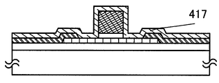
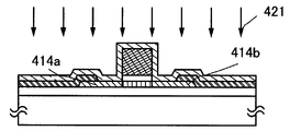
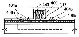
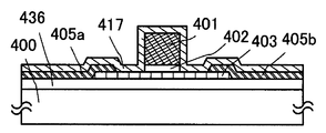
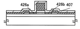
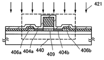
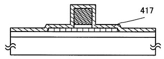
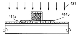
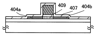
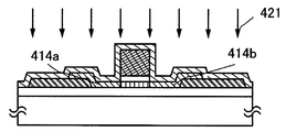
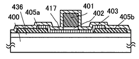
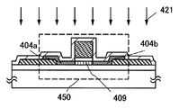
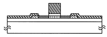
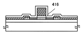
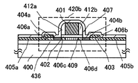
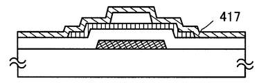
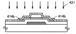
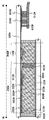
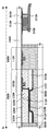
도 2a 내지 도 2d는 반도체 장치 및 반도체 장치의 제작 방법의 일 형태를 설명하기 위한 도면.
도 3a 내지 도 3f는 반도체 장치 및 반도체 장치의 제작 방법의 일 형태를 설명하기 위한 도면.
도 4a 내지 도 4f는 반도체 장치 및 반도체 장치의 제작 방법의 일 형태를 설명하기 위한 도면.
도 5a 내지 도 5d는 반도체 장치 및 반도체 장치의 제작 방법의 일 형태를 설명하기 위한 도면.
도 6a 내지 도 6d는 반도체 장치 및 반도체 장치의 제작 방법의 일 형태를 설명하기 위한 도면.
도 7a 및 도 7b는 반도체 장치의 일 형태를 설명하기 위한 도면.
도 8a 내지 도 8f는 반도체 장치 및 반도체 장치의 제작 방법의 일 형태를 설명하기 위한 도면.
도 9a 내지 도 9c는 반도체 장치의 일 형태를 설명하기 위한 도면.
도 10a 및 도 10b는 반도체 장치의 일 형태를 설명하기 위한 도면.
도 11a 및 도 11b는 반도체 장치의 일 형태를 설명하기 위한 도면.
도 12a 내지 도 12c는 반도체 장치의 일 형태를 설명하기 위한 도면.
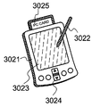
도 13a 내지 도 13f는 전자 기기를 도시한 도면.

108: 게이트 절연막
110: 게이트 전극
116: 채널 형성 영역
120: 불순물 영역
124: 금속 화합물 영역
128: 절연막
130: 절연막
140: 트랜지스터
142a: 소스 전극 또는 드레인 전극
142b: 소스 전극 또는 드레인 전극
144: 산화물 반도체막
146: 게이트 절연막
148: 게이트 전극층
150: 금속 원소를 함유한 막
152: 절연막
153: 전극층
156: 배선
162: 트랜지스터
164: 용량 소자
185: 기판
400: 기판
401: 게이트 전극층
402: 게이트 절연막
403: 산화물 반도체막
404a: 저저항 영역
404b: 저저항 영역
405a: 소스 전극층
405b: 드레인 전극층
406a: 저저항 영역
406b: 저저항 영역
406c: 저저항 영역
406d: 저저항 영역
407: 금속 원소를 함유한 막
409: 채널 형성 영역
410: 트랜지스터
412a: 측벽 절연층
412b: 측벽 절연층
414a: 저저항 영역
414b: 저저항 영역
415: 평탄화 절연막
416: 절연막
426a: 저저항 영역
426b: 저저항 영역
417: 금속 원소를 함유한 막
420a: 트랜지스터
420b: 트랜지스터
421: 도펀트
427: 절연막
436: 절연막
440: 트랜지스터
442: 게이트 절연막
445: 트랜지스터
450: 트랜지스터
465a: 배선층
465b: 배선층
601: 기판
602: 포토다이오드
606a: 반도체막
606b: 반도체막
606c: 반도체막
608: 접착층
613: 기판
631: 절연막
633: 층간 절연막
634: 층간 절연막
640: 트랜지스터
641: 전극층
642: 전극층
643: 도전층
645: 도전층
656: 트랜지스터
658: 포토다이오드 리셋 신호선
659: 게이트 신호선
671: 포토센서 출력 신호선
672: 포토센서 기준 신호선
2701: 하우징
2703: 하우징
2705: 표시부
2707: 표시부
2711: 축부
2721: 전원
2723: 조작키
2725: 스피커
2800: 하우징
2801: 하우징
2802: 표시 패널
2803: 스피커
2804: 마이크로폰
2805: 조작키
2806: 포인팅 디바이스
2807: 카메라용 렌즈
2808: 외부 접속 단자
2810: 태양 전지 셀
2811: 외부 메모리 슬롯
3001: 본체
3002: 하우징
3003: 표시부
3004: 키보드
3021: 본체
3022: 스타일러스(stylus)
3023: 표시부
3024: 조작 버튼
3025: 외부 인터페이스
3051: 본체
3053: 접안부
3054: 조작 스위치
3056: 배터리
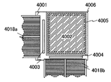
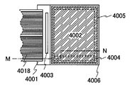
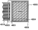
4001: 제 1 기판
4002: 화소부
4003: 신호선 구동 회로
4004: 주사선 구동 회로
4005: 씰재
4006: 제 2 기판
4008: 액정층
4010: 트랜지스터
4011: 트랜지스터
4013: 액정 소자
4015: 접속 단자 전극
4016: 단자 전극
4018: FPC
4019: 이방성 도전막
4020: 절연막
4021: 절연막
4023: 절연막
4030: 제 1 전극층
4031: 제 2 전극층
4032: 절연막
4033: 절연막
4510: 격벽
4511: 전계 발광층
4513: 발광 소자
4514: 충전재
9601: 하우징
9603: 표시부
9605: 스탠드
Claims (1)
- 반도체 장치로서,
제1 영역, 제2 영역 및 제3 영역을 포함하는 산화물 반도체층;
상기 산화물 반도체층 위의 게이트 전극층;
상기 게이트 전극층의 측면 위의 측벽 절연체; 및
상기 산화물 반도체층, 상기 게이트 전극층 및 상기 측벽 절연체 위의 질화층
을 포함하고,
상기 질화층은 금속 원소를 포함하고,
상기 질화층은 절연막이고,
상기 제2 영역은 상기 제1 영역과 상기 제3 영역 사이에 있고,
상기 제1 영역은 채널 형성 영역을 포함하고,
상기 채널 형성 영역 및 상기 게이트 전극층은 서로 중첩하고,
상기 측벽 절연체 및 상기 제2 영역은 서로 중첩하고,
상기 제2 영역의 저항은 상기 제1 영역의 저항보다 낮고,
상기 제3 영역의 저항은 상기 제2 영역의 상기 저항보다 낮고,
상기 제3 영역은 상기 질화층과 접촉하고,
상기 제3 영역은 상기 금속 원소 및 도펀트를 함유하고,
상기 제3 영역 내 상기 금속 원소의 농도는 상기 제2 영역 내 상기 금속 원소의 농도 및 상기 채널 형성 영역 내 상기 금속 원소의 농도보다 높고,
상기 제2 영역은 상기 도펀트를 함유하고,
상기 제2 영역 내 상기 도펀트의 농도 및 상기 제3 영역 내 상기 도펀트의 농도는 각각 상기 채널 형성 영역 내 상기 도펀트의 농도보다 높고,
상기 금속 원소는 알루미늄, 티타늄, 몰리브덴, 텅스텐, 하프늄, 탄탈, 란탄, 바륨, 마그네슘, 지르코늄, 및 니켈로 이루어진 그룹으로부터 선택되는 하나 이상이고,
상기 도펀트는 인, 비소, 안티몬, 붕소, 질소, 아르곤, 헬륨, 네온, 불소, 및 염소 중 하나 이상인, 반도체 장치.
Applications Claiming Priority (2)
| Application Number | Priority Date | Filing Date | Title |
|---|---|---|---|
| JP2011129976 | 2011-06-10 | ||
| JPJP-P-2011-129976 | 2011-06-10 |
Related Parent Applications (1)
| Application Number | Title | Priority Date | Filing Date |
|---|---|---|---|
| KR1020160016143A Division KR102112302B1 (ko) | 2011-06-10 | 2016-02-12 | 반도체 장치의 제작 방법 |
Publications (2)
| Publication Number | Publication Date |
|---|---|
| KR20200054931A true KR20200054931A (ko) | 2020-05-20 |
| KR102188546B1 KR102188546B1 (ko) | 2020-12-08 |
Family
ID=47293530
Family Applications (3)
| Application Number | Title | Priority Date | Filing Date |
|---|---|---|---|
| KR1020120060780A Expired - Fee Related KR102069385B1 (ko) | 2011-06-10 | 2012-06-07 | 반도체 장치의 제작 방법 |
| KR1020160016143A Expired - Fee Related KR102112302B1 (ko) | 2011-06-10 | 2016-02-12 | 반도체 장치의 제작 방법 |
| KR1020200056653A Expired - Fee Related KR102188546B1 (ko) | 2011-06-10 | 2020-05-12 | 반도체 장치의 제작 방법 |
Family Applications Before (2)
| Application Number | Title | Priority Date | Filing Date |
|---|---|---|---|
| KR1020120060780A Expired - Fee Related KR102069385B1 (ko) | 2011-06-10 | 2012-06-07 | 반도체 장치의 제작 방법 |
| KR1020160016143A Expired - Fee Related KR102112302B1 (ko) | 2011-06-10 | 2016-02-12 | 반도체 장치의 제작 방법 |
Country Status (4)
| Country | Link |
|---|---|
| US (3) | US9287407B2 (ko) |
| JP (11) | JP6005401B2 (ko) |
| KR (3) | KR102069385B1 (ko) |
| TW (8) | TWI581339B (ko) |
Families Citing this family (82)
| Publication number | Priority date | Publication date | Assignee | Title |
|---|---|---|---|---|
| JP6009226B2 (ja) | 2011-06-10 | 2016-10-19 | 株式会社半導体エネルギー研究所 | 半導体装置の作製方法 |
| US8673426B2 (en) * | 2011-06-29 | 2014-03-18 | Semiconductor Energy Laboratory Co., Ltd. | Driver circuit, method of manufacturing the driver circuit, and display device including the driver circuit |
| JP6013685B2 (ja) | 2011-07-22 | 2016-10-25 | 株式会社半導体エネルギー研究所 | 半導体装置 |
| US8994019B2 (en) | 2011-08-05 | 2015-03-31 | Semiconductor Energy Laboratory Co., Ltd. | Semiconductor device |
| US9082663B2 (en) | 2011-09-16 | 2015-07-14 | Semiconductor Energy Laboratory Co., Ltd. | Semiconductor device and manufacturing method thereof |
| US8952379B2 (en) | 2011-09-16 | 2015-02-10 | Semiconductor Energy Laboratory Co., Ltd. | Semiconductor device |
| WO2013039126A1 (en) | 2011-09-16 | 2013-03-21 | Semiconductor Energy Laboratory Co., Ltd. | Semiconductor device |
| US9431545B2 (en) | 2011-09-23 | 2016-08-30 | Semiconductor Energy Laboratory Co., Ltd. | Semiconductor device and method for manufacturing the same |
| JP5912394B2 (ja) | 2011-10-13 | 2016-04-27 | 株式会社半導体エネルギー研究所 | 半導体装置 |
| US8637864B2 (en) | 2011-10-13 | 2014-01-28 | Semiconductor Energy Laboratory Co., Ltd. | Semiconductor device and method of manufacturing the same |
| WO2013061895A1 (en) * | 2011-10-28 | 2013-05-02 | Semiconductor Energy Laboratory Co., Ltd. | Semiconductor device and manufacturing method thereof |
| US9653614B2 (en) | 2012-01-23 | 2017-05-16 | Semiconductor Energy Laboratory Co., Ltd. | Semiconductor device and method for manufacturing the same |
| US9419146B2 (en) | 2012-01-26 | 2016-08-16 | Semiconductor Energy Laboratory Co., Ltd. | Semiconductor device and method for manufacturing the same |
| US8956912B2 (en) | 2012-01-26 | 2015-02-17 | Semiconductor Energy Laboratory Co., Ltd. | Method for manufacturing semiconductor device |
| US8916424B2 (en) | 2012-02-07 | 2014-12-23 | Semiconductor Energy Laboratory Co., Ltd. | Method for manufacturing semiconductor device |
| JP6019331B2 (ja) * | 2012-03-05 | 2016-11-02 | 株式会社Joled | トランジスタ、半導体装置、表示装置および電子機器、並びに半導体装置の製造方法 |
| US20130221345A1 (en) * | 2012-02-28 | 2013-08-29 | Semiconductor Energy Laboratory Co., Ltd. | Semiconductor device and method for manufacturing the same |
| KR20130136063A (ko) | 2012-06-04 | 2013-12-12 | 삼성디스플레이 주식회사 | 박막 트랜지스터, 이를 포함하는 박막 트랜지스터 표시판 및 그 제조 방법 |
| US9488315B2 (en) | 2013-03-15 | 2016-11-08 | Applied Materials, Inc. | Gas distribution apparatus for directional and proportional delivery of process gas to a process chamber |
| KR102089314B1 (ko) * | 2013-05-14 | 2020-04-14 | 엘지디스플레이 주식회사 | 산화물 박막 트랜지스터 및 그 제조방법 |
| KR102044667B1 (ko) * | 2013-05-28 | 2019-11-14 | 엘지디스플레이 주식회사 | 산화물 박막 트랜지스터를 구비한 평판표시장치 및 그의 제조방법 |
| US9806198B2 (en) | 2013-06-05 | 2017-10-31 | Semiconductor Energy Laboratory Co., Ltd. | Semiconductor device and method for manufacturing the same |
| US9773915B2 (en) * | 2013-06-11 | 2017-09-26 | Semiconductor Energy Laboratory Co., Ltd. | Semiconductor device and manufacturing method thereof |
| US9590109B2 (en) * | 2013-08-30 | 2017-03-07 | Semiconductor Energy Laboratory Co., Ltd. | Semiconductor device and method for manufacturing the same |
| CN103500710B (zh) * | 2013-10-11 | 2015-11-25 | 京东方科技集团股份有限公司 | 一种薄膜晶体管制作方法、薄膜晶体管及显示设备 |
| US9455349B2 (en) * | 2013-10-22 | 2016-09-27 | Semiconductor Energy Laboratory Co., Ltd. | Oxide semiconductor thin film transistor with reduced impurity diffusion |
| JP2016027597A (ja) | 2013-12-06 | 2016-02-18 | 株式会社半導体エネルギー研究所 | 半導体装置 |
| US9960280B2 (en) | 2013-12-26 | 2018-05-01 | Semiconductor Energy Laboratory Co., Ltd. | Semiconductor device |
| US9577110B2 (en) * | 2013-12-27 | 2017-02-21 | Semiconductor Energy Laboratory Co., Ltd. | Semiconductor device including an oxide semiconductor and the display device including the semiconductor device |
| US9397149B2 (en) | 2013-12-27 | 2016-07-19 | Semiconductor Energy Laboratory Co., Ltd. | Semiconductor device |
| JP6506545B2 (ja) | 2013-12-27 | 2019-04-24 | 株式会社半導体エネルギー研究所 | 半導体装置 |
| KR20220046701A (ko) | 2013-12-27 | 2022-04-14 | 가부시키가이샤 한도오따이 에네루기 켄큐쇼 | 발광 장치 |
| KR102306200B1 (ko) * | 2014-01-24 | 2021-09-30 | 가부시키가이샤 한도오따이 에네루기 켄큐쇼 | 반도체 장치 |
| US9443876B2 (en) | 2014-02-05 | 2016-09-13 | Semiconductor Energy Laboratory Co., Ltd. | Semiconductor device, display device including the semiconductor device, display module including the display device, and electronic device including the semiconductor device, the display device, and the display module |
| JP6585354B2 (ja) * | 2014-03-07 | 2019-10-02 | 株式会社半導体エネルギー研究所 | 半導体装置 |
| JP6559444B2 (ja) | 2014-03-14 | 2019-08-14 | 株式会社半導体エネルギー研究所 | 半導体装置の作製方法 |
| US9515661B2 (en) * | 2014-05-09 | 2016-12-06 | Semiconductor Energy Laboratory Co., Ltd. | Circuit, semiconductor device, and clock tree |
| TWI669761B (zh) | 2014-05-30 | 2019-08-21 | 日商半導體能源研究所股份有限公司 | 半導體裝置、包括該半導體裝置的顯示裝置 |
| JP6527416B2 (ja) * | 2014-07-29 | 2019-06-05 | 株式会社半導体エネルギー研究所 | 半導体装置の作製方法 |
| JP2016111105A (ja) * | 2014-12-03 | 2016-06-20 | 株式会社Joled | 薄膜トランジスタ及びその製造方法、並びに、表示装置 |
| JP6519073B2 (ja) * | 2014-12-03 | 2019-05-29 | 株式会社Joled | 薄膜トランジスタ及びその製造方法、並びに、表示装置 |
| US9685560B2 (en) | 2015-03-02 | 2017-06-20 | Semiconductor Energy Laboratory Co., Ltd. | Transistor, method for manufacturing transistor, semiconductor device, and electronic device |
| US10147823B2 (en) | 2015-03-19 | 2018-12-04 | Semiconductor Energy Laboratory Co., Ltd. | Semiconductor device |
| KR20160137129A (ko) * | 2015-05-22 | 2016-11-30 | 엘지디스플레이 주식회사 | 박막트랜지스터, 그를 포함하는 표시 장치 및 그 박막트랜지스터의 제조 방법 |
| US9837547B2 (en) | 2015-05-22 | 2017-12-05 | Semiconductor Energy Laboratory Co., Ltd. | Semiconductor device comprising oxide conductor and display device including the semiconductor device |
| JP2016225505A (ja) * | 2015-06-01 | 2016-12-28 | 株式会社神戸製鋼所 | 薄膜トランジスタおよびその製造方法ならびにスパッタリングターゲット |
| US11024725B2 (en) | 2015-07-24 | 2021-06-01 | Semiconductor Energy Laboratory Co., Ltd. | Semiconductor device including metal oxide film |
| US9768254B2 (en) | 2015-07-30 | 2017-09-19 | International Business Machines Corporation | Leakage-free implantation-free ETSOI transistors |
| JP6725357B2 (ja) * | 2015-08-03 | 2020-07-15 | 株式会社半導体エネルギー研究所 | 半導体装置、半導体装置の作製方法 |
| TWI649875B (zh) * | 2015-08-28 | 2019-02-01 | 聯華電子股份有限公司 | 半導體元件及其製造方法 |
| JP6851166B2 (ja) | 2015-10-12 | 2021-03-31 | 株式会社半導体エネルギー研究所 | 半導体装置の作製方法 |
| KR102558900B1 (ko) * | 2015-10-23 | 2023-07-25 | 엘지디스플레이 주식회사 | 표시장치와 이의 제조방법 |
| WO2018051208A1 (en) | 2016-09-14 | 2018-03-22 | Semiconductor Energy Laboratory Co., Ltd. | Semiconductor device and manufacturing method of the same |
| JP6894726B2 (ja) * | 2017-03-10 | 2021-06-30 | 株式会社半導体エネルギー研究所 | 半導体装置、および半導体装置の作製方法 |
| TWI622844B (zh) | 2017-03-29 | 2018-05-01 | 友達光電股份有限公司 | 畫素單元與其製造方法 |
| CN107146816B (zh) * | 2017-04-10 | 2020-05-15 | 华南理工大学 | 一种氧化物半导体薄膜及由其制备的薄膜晶体管 |
| WO2018211351A1 (en) | 2017-05-19 | 2018-11-22 | Semiconductor Energy Laboratory Co., Ltd. | Semiconductor device, display device, and method for manufacturing semiconductor device |
| JP6887307B2 (ja) * | 2017-05-19 | 2021-06-16 | ルネサスエレクトロニクス株式会社 | 半導体装置の製造方法 |
| JP7235410B2 (ja) | 2017-06-27 | 2023-03-08 | 株式会社半導体エネルギー研究所 | 半導体装置 |
| US11195758B2 (en) | 2017-09-05 | 2021-12-07 | Semiconductor Energy Laboratory Co., Ltd. | Semiconductor device and method for manufacturing semiconductor device having plurality of insulator |
| US20200266289A1 (en) | 2017-09-05 | 2020-08-20 | Semiconductor Energy Laboratory Co., Ltd. | Semiconductor device and method for manufacturing semiconductor device |
| KR102669811B1 (ko) | 2017-10-20 | 2024-05-28 | 가부시키가이샤 한도오따이 에네루기 켄큐쇼 | 반도체 장치, 및 반도체 장치의 제작 방법 |
| US11545580B2 (en) * | 2017-11-15 | 2023-01-03 | South China University Of Technology | Metal oxide (MO semiconductor and thin-film transistor and application thereof |
| US20190267402A1 (en) * | 2018-02-26 | 2019-08-29 | Shenzhen China Star Optoelectronics Semiconductor Display Technology Co., Ltd. | Array substrate and manufacturing method for the same |
| JPWO2020012276A1 (ja) | 2018-07-09 | 2021-08-12 | 株式会社半導体エネルギー研究所 | 半導体装置 |
| US12439742B2 (en) * | 2018-09-26 | 2025-10-07 | Idemitsu Kosan Co., Ltd. | Light emitting device with electrode having specified molar ratio of magnesium to zinc |
| KR102948551B1 (ko) * | 2019-06-14 | 2026-04-03 | 가부시키가이샤 한도오따이 에네루기 켄큐쇼 | 반도체 장치 및 반도체 장치의 제작 방법 |
| DE102021101243A1 (de) * | 2020-05-29 | 2021-12-02 | Taiwan Semiconductor Manufacturing Co., Ltd. | Speicherblock-kanalregionen |
| US11695073B2 (en) | 2020-05-29 | 2023-07-04 | Taiwan Semiconductor Manufacturing Co., Ltd. | Memory array gate structures |
| DE102020127831A1 (de) | 2020-05-29 | 2021-12-02 | Taiwan Semiconductor Manufacturing Co., Ltd. | Speicherarray-gatestrukturen |
| US11710790B2 (en) | 2020-05-29 | 2023-07-25 | Taiwan Semiconductor Manufacturing Company, Ltd. | Memory array channel regions |
| US11729987B2 (en) | 2020-06-30 | 2023-08-15 | Taiwan Semiconductor Manufacturing Company, Ltd. | Memory array source/drain electrode structures |
| US11640974B2 (en) | 2020-06-30 | 2023-05-02 | Taiwan Semiconductor Manufacturing Co., Ltd. | Memory array isolation structures |
| US11355516B2 (en) | 2020-07-16 | 2022-06-07 | Taiwan Semiconductor Manufacturing Co., Ltd. | Three-dimensional memory device and method |
| US11647634B2 (en) | 2020-07-16 | 2023-05-09 | Taiwan Semiconductor Manufacturing Co., Ltd. | Three-dimensional memory device and method |
| JPWO2022176386A1 (ko) * | 2021-02-18 | 2022-08-25 | ||
| US12009432B2 (en) | 2021-03-05 | 2024-06-11 | Semiconductor Energy Laboratory Co., Ltd. | Transistor and display device |
| US20250294883A1 (en) * | 2022-06-30 | 2025-09-18 | Sharp Display Technology Corporation | Display device and method for manufacturing same |
| KR20240077525A (ko) * | 2022-11-22 | 2024-06-03 | 삼성디스플레이 주식회사 | 표시패널, 이에 포함되는 박막 트랜지스터, 및 이의 제조 방법 |
| TWI852648B (zh) * | 2023-06-26 | 2024-08-11 | 國立陽明交通大學 | 增強型場效電晶體的製法 |
| TWI855815B (zh) * | 2023-08-09 | 2024-09-11 | 力晶積成電子製造股份有限公司 | 影像感測器 |
| TWI874057B (zh) * | 2023-12-20 | 2025-02-21 | 友達光電股份有限公司 | 半導體裝置及其製造方法 |
Citations (4)
| Publication number | Priority date | Publication date | Assignee | Title |
|---|---|---|---|---|
| JP2006100760A (ja) * | 2004-09-02 | 2006-04-13 | Casio Comput Co Ltd | 薄膜トランジスタおよびその製造方法 |
| KR20080086815A (ko) * | 2007-03-23 | 2008-09-26 | 가부시키가이샤 한도오따이 에네루기 켄큐쇼 | 반도체장치 및 그 제조 방법 |
| JP2010093070A (ja) * | 2008-10-08 | 2010-04-22 | Canon Inc | 電界効果型トランジスタ及びその製造方法 |
| JP2010205987A (ja) * | 2009-03-04 | 2010-09-16 | Sony Corp | 薄膜トランジスタおよびその製造方法並びに表示装置 |
Family Cites Families (145)
| Publication number | Priority date | Publication date | Assignee | Title |
|---|---|---|---|---|
| JPS60198861A (ja) | 1984-03-23 | 1985-10-08 | Fujitsu Ltd | 薄膜トランジスタ |
| JPH0244256B2 (ja) | 1987-01-28 | 1990-10-03 | Kagaku Gijutsucho Mukizaishitsu Kenkyushocho | Ingazn2o5deshimesarerurotsuhoshokeinosojokozoojusurukagobutsuoyobisonoseizoho |
| JPS63210023A (ja) | 1987-02-24 | 1988-08-31 | Natl Inst For Res In Inorg Mater | InGaZn↓4O↓7で示される六方晶系の層状構造を有する化合物およびその製造法 |
| JPH0244260B2 (ja) | 1987-02-24 | 1990-10-03 | Kagaku Gijutsucho Mukizaishitsu Kenkyushocho | Ingazn5o8deshimesarerurotsuhoshokeinosojokozoojusurukagobutsuoyobisonoseizoho |
| JPH0244258B2 (ja) | 1987-02-24 | 1990-10-03 | Kagaku Gijutsucho Mukizaishitsu Kenkyushocho | Ingazn3o6deshimesarerurotsuhoshokeinosojokozoojusurukagobutsuoyobisonoseizoho |
| JPH0244262B2 (ja) | 1987-02-27 | 1990-10-03 | Kagaku Gijutsucho Mukizaishitsu Kenkyushocho | Ingazn6o9deshimesarerurotsuhoshokeinosojokozoojusurukagobutsuoyobisonoseizoho |
| JPH0244263B2 (ja) | 1987-04-22 | 1990-10-03 | Kagaku Gijutsucho Mukizaishitsu Kenkyushocho | Ingazn7o10deshimesarerurotsuhoshokeinosojokozoojusurukagobutsuoyobisonoseizoho |
| JPH05251705A (ja) | 1992-03-04 | 1993-09-28 | Fuji Xerox Co Ltd | 薄膜トランジスタ |
| JPH06112222A (ja) * | 1992-09-28 | 1994-04-22 | Seiko Epson Corp | 薄膜半導体装置及びその製造方法 |
| JP3479375B2 (ja) | 1995-03-27 | 2003-12-15 | 科学技術振興事業団 | 亜酸化銅等の金属酸化物半導体による薄膜トランジスタとpn接合を形成した金属酸化物半導体装置およびそれらの製造方法 |
| JPH11505377A (ja) | 1995-08-03 | 1999-05-18 | フィリップス エレクトロニクス ネムローゼ フェンノートシャップ | 半導体装置 |
| JP3625598B2 (ja) | 1995-12-30 | 2005-03-02 | 三星電子株式会社 | 液晶表示装置の製造方法 |
| US6197624B1 (en) * | 1997-08-29 | 2001-03-06 | Semiconductor Energy Laboratory Co., Ltd. | Method of adjusting the threshold voltage in an SOI CMOS |
| JP4170454B2 (ja) | 1998-07-24 | 2008-10-22 | Hoya株式会社 | 透明導電性酸化物薄膜を有する物品及びその製造方法 |
| JP2000150861A (ja) | 1998-11-16 | 2000-05-30 | Tdk Corp | 酸化物薄膜 |
| JP3276930B2 (ja) | 1998-11-17 | 2002-04-22 | 科学技術振興事業団 | トランジスタ及び半導体装置 |
| JP2001053164A (ja) * | 1999-08-04 | 2001-02-23 | Sony Corp | 半導体記憶装置 |
| TW460731B (en) | 1999-09-03 | 2001-10-21 | Ind Tech Res Inst | Electrode structure and production method of wide viewing angle LCD |
| JP4089858B2 (ja) | 2000-09-01 | 2008-05-28 | 国立大学法人東北大学 | 半導体デバイス |
| JP2002093924A (ja) * | 2000-09-20 | 2002-03-29 | Sony Corp | 半導体記憶装置 |
| JP2003050405A (ja) * | 2000-11-15 | 2003-02-21 | Matsushita Electric Ind Co Ltd | 薄膜トランジスタアレイ、その製造方法およびそれを用いた表示パネル |
| KR20020038482A (ko) | 2000-11-15 | 2002-05-23 | 모리시타 요이찌 | 박막 트랜지스터 어레이, 그 제조방법 및 그것을 이용한표시패널 |
| JP3997731B2 (ja) | 2001-03-19 | 2007-10-24 | 富士ゼロックス株式会社 | 基材上に結晶性半導体薄膜を形成する方法 |
| JP2002289859A (ja) | 2001-03-23 | 2002-10-04 | Minolta Co Ltd | 薄膜トランジスタ |
| JP3925839B2 (ja) | 2001-09-10 | 2007-06-06 | シャープ株式会社 | 半導体記憶装置およびその試験方法 |
| JP4090716B2 (ja) | 2001-09-10 | 2008-05-28 | 雅司 川崎 | 薄膜トランジスタおよびマトリクス表示装置 |
| JP4164562B2 (ja) | 2002-09-11 | 2008-10-15 | 独立行政法人科学技術振興機構 | ホモロガス薄膜を活性層として用いる透明薄膜電界効果型トランジスタ |
| EP1443130B1 (en) | 2001-11-05 | 2011-09-28 | Japan Science and Technology Agency | Natural superlattice homologous single crystal thin film, method for preparation thereof, and device using said single crystal thin film |
| JP4083486B2 (ja) | 2002-02-21 | 2008-04-30 | 独立行政法人科学技術振興機構 | LnCuO(S,Se,Te)単結晶薄膜の製造方法 |
| US7049190B2 (en) | 2002-03-15 | 2006-05-23 | Sanyo Electric Co., Ltd. | Method for forming ZnO film, method for forming ZnO semiconductor layer, method for fabricating semiconductor device, and semiconductor device |
| JP3933591B2 (ja) | 2002-03-26 | 2007-06-20 | 淳二 城戸 | 有機エレクトロルミネッセント素子 |
| US7339187B2 (en) | 2002-05-21 | 2008-03-04 | State Of Oregon Acting By And Through The Oregon State Board Of Higher Education On Behalf Of Oregon State University | Transistor structures |
| US6949473B2 (en) * | 2002-05-24 | 2005-09-27 | Finisar Corporation | Methods for identifying and removing an oxide-induced dead zone in a semiconductor device structure |
| JP2004022625A (ja) | 2002-06-13 | 2004-01-22 | Murata Mfg Co Ltd | 半導体デバイス及び該半導体デバイスの製造方法 |
| US7105868B2 (en) | 2002-06-24 | 2006-09-12 | Cermet, Inc. | High-electron mobility transistor with zinc oxide |
| US7067843B2 (en) | 2002-10-11 | 2006-06-27 | E. I. Du Pont De Nemours And Company | Transparent oxide semiconductor thin film transistors |
| EP1565934A1 (en) * | 2002-11-29 | 2005-08-24 | Advanced Micro Devices, Inc. | Drain/source extension structure of a field effect transistor including doped high-k sidewall spacers |
| DE10255849B4 (de) | 2002-11-29 | 2006-06-14 | Advanced Micro Devices, Inc., Sunnyvale | Verbesserte Drain/Source-Erweiterungsstruktur eines Feldeffekttransistors mit dotierten Seitenwandabstandselementen mit hoher Permittivität und Verfahren zu deren Herstellung |
| JP4166105B2 (ja) | 2003-03-06 | 2008-10-15 | シャープ株式会社 | 半導体装置およびその製造方法 |
| JP2004273732A (ja) | 2003-03-07 | 2004-09-30 | Sharp Corp | アクティブマトリクス基板およびその製造方法 |
| JP4108633B2 (ja) | 2003-06-20 | 2008-06-25 | シャープ株式会社 | 薄膜トランジスタおよびその製造方法ならびに電子デバイス |
| US7262463B2 (en) | 2003-07-25 | 2007-08-28 | Hewlett-Packard Development Company, L.P. | Transistor including a deposited channel region having a doped portion |
| US7297977B2 (en) | 2004-03-12 | 2007-11-20 | Hewlett-Packard Development Company, L.P. | Semiconductor device |
| US7282782B2 (en) | 2004-03-12 | 2007-10-16 | Hewlett-Packard Development Company, L.P. | Combined binary oxide semiconductor device |
| EP1737044B1 (en) | 2004-03-12 | 2014-12-10 | Japan Science and Technology Agency | Amorphous oxide and thin film transistor |
| US7145174B2 (en) | 2004-03-12 | 2006-12-05 | Hewlett-Packard Development Company, Lp. | Semiconductor device |
| US7211825B2 (en) | 2004-06-14 | 2007-05-01 | Yi-Chi Shih | Indium oxide-based thin film transistors and circuits |
| US7285501B2 (en) | 2004-09-17 | 2007-10-23 | Hewlett-Packard Development Company, L.P. | Method of forming a solution processed device |
| US7298084B2 (en) | 2004-11-02 | 2007-11-20 | 3M Innovative Properties Company | Methods and displays utilizing integrated zinc oxide row and column drivers in conjunction with organic light emitting diodes |
| JP5138163B2 (ja) * | 2004-11-10 | 2013-02-06 | キヤノン株式会社 | 電界効果型トランジスタ |
| US7829444B2 (en) | 2004-11-10 | 2010-11-09 | Canon Kabushiki Kaisha | Field effect transistor manufacturing method |
| EP1815530B1 (en) | 2004-11-10 | 2021-02-17 | Canon Kabushiki Kaisha | Field effect transistor employing an amorphous oxide |
| US7453065B2 (en) | 2004-11-10 | 2008-11-18 | Canon Kabushiki Kaisha | Sensor and image pickup device |
| US7863611B2 (en) | 2004-11-10 | 2011-01-04 | Canon Kabushiki Kaisha | Integrated circuits utilizing amorphous oxides |
| RU2358354C2 (ru) | 2004-11-10 | 2009-06-10 | Кэнон Кабусики Кайся | Светоизлучающее устройство |
| KR100998527B1 (ko) | 2004-11-10 | 2010-12-07 | 고쿠리츠다이가쿠호진 토쿄고교 다이가꾸 | 비정질 산화물 및 전계 효과 트랜지스터 |
| US7791072B2 (en) | 2004-11-10 | 2010-09-07 | Canon Kabushiki Kaisha | Display |
| US7579224B2 (en) | 2005-01-21 | 2009-08-25 | Semiconductor Energy Laboratory Co., Ltd. | Method for manufacturing a thin film semiconductor device |
| TWI505473B (zh) | 2005-01-28 | 2015-10-21 | 半導體能源研究所股份有限公司 | 半導體裝置,電子裝置,和半導體裝置的製造方法 |
| TWI481024B (zh) | 2005-01-28 | 2015-04-11 | 半導體能源研究所股份有限公司 | 半導體裝置,電子裝置,和半導體裝置的製造方法 |
| US7858451B2 (en) | 2005-02-03 | 2010-12-28 | Semiconductor Energy Laboratory Co., Ltd. | Electronic device, semiconductor device and manufacturing method thereof |
| US7948171B2 (en) | 2005-02-18 | 2011-05-24 | Semiconductor Energy Laboratory Co., Ltd. | Light emitting device |
| US20060205129A1 (en) * | 2005-02-25 | 2006-09-14 | Semiconductor Energy Laboratory Co., Ltd. | Method for manufacturing semiconductor device |
| US20060197092A1 (en) | 2005-03-03 | 2006-09-07 | Randy Hoffman | System and method for forming conductive material on a substrate |
| JP2006245260A (ja) * | 2005-03-03 | 2006-09-14 | Seiko Epson Corp | 半導体装置の製造方法、電気光学装置の製造方法、半導体装置、及び電気光学装置、並びに電子機器 |
| US8681077B2 (en) | 2005-03-18 | 2014-03-25 | Semiconductor Energy Laboratory Co., Ltd. | Semiconductor device, and display device, driving method and electronic apparatus thereof |
| US7544967B2 (en) | 2005-03-28 | 2009-06-09 | Massachusetts Institute Of Technology | Low voltage flexible organic/transparent transistor for selective gas sensing, photodetecting and CMOS device applications |
| US7645478B2 (en) | 2005-03-31 | 2010-01-12 | 3M Innovative Properties Company | Methods of making displays |
| US8300031B2 (en) | 2005-04-20 | 2012-10-30 | Semiconductor Energy Laboratory Co., Ltd. | Semiconductor device comprising transistor having gate and drain connected through a current-voltage conversion element |
| JP2006344849A (ja) | 2005-06-10 | 2006-12-21 | Casio Comput Co Ltd | 薄膜トランジスタ |
| US7402506B2 (en) | 2005-06-16 | 2008-07-22 | Eastman Kodak Company | Methods of making thin film transistors comprising zinc-oxide-based semiconductor materials and transistors made thereby |
| US7691666B2 (en) | 2005-06-16 | 2010-04-06 | Eastman Kodak Company | Methods of making thin film transistors comprising zinc-oxide-based semiconductor materials and transistors made thereby |
| US7507618B2 (en) | 2005-06-27 | 2009-03-24 | 3M Innovative Properties Company | Method for making electronic devices using metal oxide nanoparticles |
| KR100711890B1 (ko) | 2005-07-28 | 2007-04-25 | 삼성에스디아이 주식회사 | 유기 발광표시장치 및 그의 제조방법 |
| JP2007059128A (ja) | 2005-08-23 | 2007-03-08 | Canon Inc | 有機el表示装置およびその製造方法 |
| JP4280736B2 (ja) | 2005-09-06 | 2009-06-17 | キヤノン株式会社 | 半導体素子 |
| JP4850457B2 (ja) | 2005-09-06 | 2012-01-11 | キヤノン株式会社 | 薄膜トランジスタ及び薄膜ダイオード |
| JP2007073705A (ja) | 2005-09-06 | 2007-03-22 | Canon Inc | 酸化物半導体チャネル薄膜トランジスタおよびその製造方法 |
| JP5116225B2 (ja) | 2005-09-06 | 2013-01-09 | キヤノン株式会社 | 酸化物半導体デバイスの製造方法 |
| EP1998373A3 (en) | 2005-09-29 | 2012-10-31 | Semiconductor Energy Laboratory Co, Ltd. | Semiconductor device having oxide semiconductor layer and manufacturing method thereof |
| JP5037808B2 (ja) | 2005-10-20 | 2012-10-03 | キヤノン株式会社 | アモルファス酸化物を用いた電界効果型トランジスタ、及び該トランジスタを用いた表示装置 |
| CN101577231B (zh) | 2005-11-15 | 2013-01-02 | 株式会社半导体能源研究所 | 半导体器件及其制造方法 |
| TWI292281B (en) | 2005-12-29 | 2008-01-01 | Ind Tech Res Inst | Pixel structure of active organic light emitting diode and method of fabricating the same |
| US7867636B2 (en) | 2006-01-11 | 2011-01-11 | Murata Manufacturing Co., Ltd. | Transparent conductive film and method for manufacturing the same |
| JP4977478B2 (ja) | 2006-01-21 | 2012-07-18 | 三星電子株式会社 | ZnOフィルム及びこれを用いたTFTの製造方法 |
| US7576394B2 (en) | 2006-02-02 | 2009-08-18 | Kochi Industrial Promotion Center | Thin film transistor including low resistance conductive thin films and manufacturing method thereof |
| US7977169B2 (en) | 2006-02-15 | 2011-07-12 | Kochi Industrial Promotion Center | Semiconductor device including active layer made of zinc oxide with controlled orientations and manufacturing method thereof |
| JP5015470B2 (ja) * | 2006-02-15 | 2012-08-29 | 財団法人高知県産業振興センター | 薄膜トランジスタ及びその製法 |
| JP5110803B2 (ja) | 2006-03-17 | 2012-12-26 | キヤノン株式会社 | 酸化物膜をチャネルに用いた電界効果型トランジスタ及びその製造方法 |
| KR20070101595A (ko) | 2006-04-11 | 2007-10-17 | 삼성전자주식회사 | ZnO TFT |
| US20070252928A1 (en) | 2006-04-28 | 2007-11-01 | Toppan Printing Co., Ltd. | Structure, transmission type liquid crystal display, reflection type display and manufacturing method thereof |
| CN101356652B (zh) | 2006-06-02 | 2012-04-18 | 日本财团法人高知县产业振兴中心 | 包括由氧化锌构成的氧化物半导体薄膜层的半导体器件及其制造方法 |
| JP5028033B2 (ja) | 2006-06-13 | 2012-09-19 | キヤノン株式会社 | 酸化物半導体膜のドライエッチング方法 |
| JP4404881B2 (ja) | 2006-08-09 | 2010-01-27 | 日本電気株式会社 | 薄膜トランジスタアレイ、その製造方法及び液晶表示装置 |
| JP4609797B2 (ja) | 2006-08-09 | 2011-01-12 | Nec液晶テクノロジー株式会社 | 薄膜デバイス及びその製造方法 |
| JP4999400B2 (ja) | 2006-08-09 | 2012-08-15 | キヤノン株式会社 | 酸化物半導体膜のドライエッチング方法 |
| JP4332545B2 (ja) | 2006-09-15 | 2009-09-16 | キヤノン株式会社 | 電界効果型トランジスタ及びその製造方法 |
| JP5164357B2 (ja) | 2006-09-27 | 2013-03-21 | キヤノン株式会社 | 半導体装置及び半導体装置の製造方法 |
| JP4274219B2 (ja) | 2006-09-27 | 2009-06-03 | セイコーエプソン株式会社 | 電子デバイス、有機エレクトロルミネッセンス装置、有機薄膜半導体装置 |
| US7622371B2 (en) | 2006-10-10 | 2009-11-24 | Hewlett-Packard Development Company, L.P. | Fused nanocrystal thin film semiconductor and method |
| US7772021B2 (en) | 2006-11-29 | 2010-08-10 | Samsung Electronics Co., Ltd. | Flat panel displays comprising a thin-film transistor having a semiconductive oxide in its channel and methods of fabricating the same for use in flat panel displays |
| JP2008140684A (ja) | 2006-12-04 | 2008-06-19 | Toppan Printing Co Ltd | カラーelディスプレイおよびその製造方法 |
| KR101303578B1 (ko) | 2007-01-05 | 2013-09-09 | 삼성전자주식회사 | 박막 식각 방법 |
| US8207063B2 (en) | 2007-01-26 | 2012-06-26 | Eastman Kodak Company | Process for atomic layer deposition |
| JP5337380B2 (ja) * | 2007-01-26 | 2013-11-06 | 株式会社半導体エネルギー研究所 | 半導体装置及びその作製方法 |
| KR100858088B1 (ko) | 2007-02-28 | 2008-09-10 | 삼성전자주식회사 | 박막 트랜지스터 및 그 제조 방법 |
| KR100851215B1 (ko) | 2007-03-14 | 2008-08-07 | 삼성에스디아이 주식회사 | 박막 트랜지스터 및 이를 이용한 유기 전계 발광표시장치 |
| US7795613B2 (en) | 2007-04-17 | 2010-09-14 | Toppan Printing Co., Ltd. | Structure with transistor |
| KR101325053B1 (ko) | 2007-04-18 | 2013-11-05 | 삼성디스플레이 주식회사 | 박막 트랜지스터 기판 및 이의 제조 방법 |
| KR20080094300A (ko) | 2007-04-19 | 2008-10-23 | 삼성전자주식회사 | 박막 트랜지스터 및 그 제조 방법과 박막 트랜지스터를포함하는 평판 디스플레이 |
| KR101334181B1 (ko) * | 2007-04-20 | 2013-11-28 | 삼성전자주식회사 | 선택적으로 결정화된 채널층을 갖는 박막 트랜지스터 및 그제조 방법 |
| WO2008133345A1 (en) | 2007-04-25 | 2008-11-06 | Canon Kabushiki Kaisha | Oxynitride semiconductor |
| KR101345376B1 (ko) | 2007-05-29 | 2013-12-24 | 삼성전자주식회사 | ZnO 계 박막 트랜지스터 및 그 제조방법 |
| KR20090002841A (ko) * | 2007-07-04 | 2009-01-09 | 삼성전자주식회사 | 산화물 반도체, 이를 포함하는 박막 트랜지스터 및 그 제조방법 |
| US7678668B2 (en) * | 2007-07-04 | 2010-03-16 | Semiconductor Energy Laboratory Co., Ltd. | Manufacturing method of SOI substrate and manufacturing method of semiconductor device |
| US7799658B2 (en) * | 2007-10-10 | 2010-09-21 | Semiconductor Energy Laboratory Co., Ltd. | Method for manufacturing semiconductor substrate and method for manufacturing semiconductor device |
| TWI362755B (en) * | 2007-11-12 | 2012-04-21 | Chunghwa Picture Tubes Ltd | Manufacturing method of thin film transistor |
| KR101375831B1 (ko) | 2007-12-03 | 2014-04-02 | 삼성전자주식회사 | 산화물 반도체 박막 트랜지스터를 이용한 디스플레이 장치 |
| JP5430846B2 (ja) * | 2007-12-03 | 2014-03-05 | 株式会社半導体エネルギー研究所 | 半導体装置の作製方法 |
| JP5213421B2 (ja) | 2007-12-04 | 2013-06-19 | キヤノン株式会社 | 酸化物半導体薄膜トランジスタ |
| KR101518091B1 (ko) | 2007-12-13 | 2015-05-06 | 이데미쓰 고산 가부시키가이샤 | 산화물 반도체를 이용한 전계 효과형 트랜지스터 및 그 제조방법 |
| US8202365B2 (en) | 2007-12-17 | 2012-06-19 | Fujifilm Corporation | Process for producing oriented inorganic crystalline film, and semiconductor device using the oriented inorganic crystalline film |
| JP5704790B2 (ja) * | 2008-05-07 | 2015-04-22 | キヤノン株式会社 | 薄膜トランジスタ、および、表示装置 |
| KR101496148B1 (ko) | 2008-05-15 | 2015-02-27 | 삼성전자주식회사 | 반도체소자 및 그 제조방법 |
| EP2297778A1 (en) * | 2008-05-23 | 2011-03-23 | Semiconductor Energy Laboratory Co, Ltd. | Semiconductor device |
| JP4623179B2 (ja) | 2008-09-18 | 2011-02-02 | ソニー株式会社 | 薄膜トランジスタおよびその製造方法 |
| WO2010032602A1 (en) * | 2008-09-18 | 2010-03-25 | Semiconductor Energy Laboratory Co., Ltd. | Semiconductor device |
| JP5451280B2 (ja) | 2008-10-09 | 2014-03-26 | キヤノン株式会社 | ウルツ鉱型結晶成長用基板およびその製造方法ならびに半導体装置 |
| JP5515281B2 (ja) * | 2008-12-03 | 2014-06-11 | ソニー株式会社 | 薄膜トランジスタ、表示装置、電子機器および薄膜トランジスタの製造方法 |
| US8367486B2 (en) * | 2009-02-05 | 2013-02-05 | Semiconductor Energy Laboratory Co., Ltd. | Transistor and method for manufacturing the transistor |
| US20100224878A1 (en) | 2009-03-05 | 2010-09-09 | Semiconductor Energy Laboratory Co., Ltd. | Semiconductor device |
| JP5760298B2 (ja) | 2009-05-21 | 2015-08-05 | ソニー株式会社 | 薄膜トランジスタ、表示装置、および電子機器 |
| KR20110003775A (ko) * | 2009-07-06 | 2011-01-13 | 주성엔지니어링(주) | 금속 산화물 반도체 박막 트랜지스터 및 이의 제조 방법 |
| KR20120051727A (ko) | 2009-07-31 | 2012-05-22 | 가부시키가이샤 한도오따이 에네루기 켄큐쇼 | 반도체 디바이스 및 그 형성 방법 |
| TWI596741B (zh) | 2009-08-07 | 2017-08-21 | 半導體能源研究所股份有限公司 | 半導體裝置和其製造方法 |
| CN104485336B (zh) | 2009-10-21 | 2018-01-02 | 株式会社半导体能源研究所 | 半导体器件 |
| KR20190006091A (ko) * | 2009-10-29 | 2019-01-16 | 가부시키가이샤 한도오따이 에네루기 켄큐쇼 | 반도체 장치 |
| KR20250075719A (ko) * | 2009-10-30 | 2025-05-28 | 가부시키가이샤 한도오따이 에네루기 켄큐쇼 | 반도체 장치 |
| KR101073272B1 (ko) * | 2009-11-04 | 2011-10-12 | 삼성모바일디스플레이주식회사 | 유기전계발광 표시 장치의 제조 방법 |
| CN102612741B (zh) * | 2009-11-06 | 2014-11-12 | 株式会社半导体能源研究所 | 半导体装置 |
| KR20190124813A (ko) * | 2009-11-20 | 2019-11-05 | 가부시키가이샤 한도오따이 에네루기 켄큐쇼 | 반도체 장치 |
| WO2011070900A1 (en) | 2009-12-08 | 2011-06-16 | Semiconductor Energy Laboratory Co., Ltd. | Semiconductor device and manufacturing method thereof |
| JP5708910B2 (ja) * | 2010-03-30 | 2015-04-30 | ソニー株式会社 | 薄膜トランジスタおよびその製造方法、並びに表示装置 |
| JP2012015436A (ja) | 2010-07-05 | 2012-01-19 | Sony Corp | 薄膜トランジスタおよび表示装置 |
| JP6019329B2 (ja) | 2011-03-31 | 2016-11-02 | 株式会社Joled | 表示装置および電子機器 |
-
2012
- 2012-05-29 JP JP2012121639A patent/JP6005401B2/ja not_active Expired - Fee Related
- 2012-05-31 US US13/484,670 patent/US9287407B2/en active Active
- 2012-06-05 TW TW105110577A patent/TWI581339B/zh not_active IP Right Cessation
- 2012-06-05 TW TW112145005A patent/TW202414610A/zh unknown
- 2012-06-05 TW TW108125823A patent/TWI754830B/zh active
- 2012-06-05 TW TW101120145A patent/TWI559407B/zh not_active IP Right Cessation
- 2012-06-05 TW TW112123210A patent/TWI894576B/zh active
- 2012-06-05 TW TW106102180A patent/TWI631628B/zh not_active IP Right Cessation
- 2012-06-05 TW TW111103172A patent/TWI828047B/zh active
- 2012-06-05 TW TW107117085A patent/TWI754751B/zh active
- 2012-06-07 KR KR1020120060780A patent/KR102069385B1/ko not_active Expired - Fee Related
-
2015
- 2015-07-08 JP JP2015136608A patent/JP6025928B2/ja not_active Expired - Fee Related
-
2016
- 2016-02-12 KR KR1020160016143A patent/KR102112302B1/ko not_active Expired - Fee Related
- 2016-02-16 US US15/044,428 patent/US9837545B2/en not_active Expired - Fee Related
- 2016-10-11 JP JP2016199903A patent/JP6291552B2/ja active Active
-
2017
- 2017-11-30 US US15/827,426 patent/US10833202B2/en active Active
-
2018
- 2018-02-09 JP JP2018021838A patent/JP6461392B2/ja not_active Expired - Fee Related
- 2018-12-25 JP JP2018240815A patent/JP6681969B2/ja not_active Expired - Fee Related
-
2020
- 2020-03-24 JP JP2020052391A patent/JP6875577B2/ja active Active
- 2020-05-12 KR KR1020200056653A patent/KR102188546B1/ko not_active Expired - Fee Related
-
2021
- 2021-04-22 JP JP2021072437A patent/JP6999848B2/ja active Active
- 2021-12-22 JP JP2021207907A patent/JP7354220B2/ja active Active
-
2023
- 2023-09-20 JP JP2023152067A patent/JP7524435B2/ja active Active
-
2024
- 2024-07-17 JP JP2024113893A patent/JP7739544B2/ja active Active
-
2025
- 2025-09-03 JP JP2025146418A patent/JP2025175013A/ja active Pending
Patent Citations (4)
| Publication number | Priority date | Publication date | Assignee | Title |
|---|---|---|---|---|
| JP2006100760A (ja) * | 2004-09-02 | 2006-04-13 | Casio Comput Co Ltd | 薄膜トランジスタおよびその製造方法 |
| KR20080086815A (ko) * | 2007-03-23 | 2008-09-26 | 가부시키가이샤 한도오따이 에네루기 켄큐쇼 | 반도체장치 및 그 제조 방법 |
| JP2010093070A (ja) * | 2008-10-08 | 2010-04-22 | Canon Inc | 電界効果型トランジスタ及びその製造方法 |
| JP2010205987A (ja) * | 2009-03-04 | 2010-09-16 | Sony Corp | 薄膜トランジスタおよびその製造方法並びに表示装置 |
Non-Patent Citations (1)
| Title |
|---|
| N. Morosawa. 등, SID 11 DIGEST pp.479-482 |
Also Published As
Similar Documents
| Publication | Publication Date | Title |
|---|---|---|
| KR102096217B1 (ko) | 반도체 장치의 제작 방법 | |
| KR102188546B1 (ko) | 반도체 장치의 제작 방법 | |
| KR102734788B1 (ko) | 반도체 장치의 제작 방법 | |
| JP6310978B2 (ja) | 半導体装置の作製方法 |
Legal Events
| Date | Code | Title | Description |
|---|---|---|---|
| A107 | Divisional application of patent | ||
| PA0107 | Divisional application |
St.27 status event code: A-0-1-A10-A16-div-PA0107 St.27 status event code: A-0-1-A10-A18-div-PA0107 |
|
| PG1501 | Laying open of application |
St.27 status event code: A-1-1-Q10-Q12-nap-PG1501 |
|
| A201 | Request for examination | ||
| P11-X000 | Amendment of application requested |
St.27 status event code: A-2-2-P10-P11-nap-X000 |
|
| P13-X000 | Application amended |
St.27 status event code: A-2-2-P10-P13-nap-X000 |
|
| PA0201 | Request for examination |
St.27 status event code: A-1-2-D10-D11-exm-PA0201 |
|
| E701 | Decision to grant or registration of patent right | ||
| PE0701 | Decision of registration |
St.27 status event code: A-1-2-D10-D22-exm-PE0701 |
|
| GRNT | Written decision to grant | ||
| PR0701 | Registration of establishment |
St.27 status event code: A-2-4-F10-F11-exm-PR0701 |
|
| PR1002 | Payment of registration fee |
Fee payment year number: 1 St.27 status event code: A-2-2-U10-U11-oth-PR1002 |
|
| PG1601 | Publication of registration |
St.27 status event code: A-4-4-Q10-Q13-nap-PG1601 |
|
| PC1903 | Unpaid annual fee |
Not in force date: 20231203 Payment event data comment text: Termination Category : DEFAULT_OF_REGISTRATION_FEE St.27 status event code: A-4-4-U10-U13-oth-PC1903 |
|
| PC1903 | Unpaid annual fee |
Ip right cessation event data comment text: Termination Category : DEFAULT_OF_REGISTRATION_FEE Not in force date: 20231203 St.27 status event code: N-4-6-H10-H13-oth-PC1903 |
|
| P22-X000 | Classification modified |
St.27 status event code: A-4-4-P10-P22-nap-X000 |
|
| P22-X000 | Classification modified |
St.27 status event code: A-4-4-P10-P22-nap-X000 |