KR20220164800A - 광대역 인덕터 - Google Patents
광대역 인덕터 Download PDFInfo
- Publication number
- KR20220164800A KR20220164800A KR1020227040090A KR20227040090A KR20220164800A KR 20220164800 A KR20220164800 A KR 20220164800A KR 1020227040090 A KR1020227040090 A KR 1020227040090A KR 20227040090 A KR20227040090 A KR 20227040090A KR 20220164800 A KR20220164800 A KR 20220164800A
- Authority
- KR
- South Korea
- Prior art keywords
- substrate
- glass
- trenches
- broadband
- inductor
- Prior art date
- Legal status (The legal status is an assumption and is not a legal conclusion. Google has not performed a legal analysis and makes no representation as to the accuracy of the status listed.)
- Ceased
Links
- 238000000034 method Methods 0.000 claims abstract description 60
- 239000003990 capacitor Substances 0.000 claims abstract description 16
- 239000000758 substrate Substances 0.000 claims description 281
- 239000006089 photosensitive glass Substances 0.000 claims description 97
- 239000011521 glass Substances 0.000 claims description 62
- 239000004020 conductor Substances 0.000 claims description 40
- 238000011049 filling Methods 0.000 claims description 38
- 229920002120 photoresistant polymer Polymers 0.000 claims description 35
- 238000010438 heat treatment Methods 0.000 claims description 30
- 239000002178 crystalline material Substances 0.000 claims description 27
- 238000001816 cooling Methods 0.000 claims description 26
- 230000009477 glass transition Effects 0.000 claims description 26
- 230000004913 activation Effects 0.000 claims description 25
- 239000000919 ceramic Substances 0.000 claims description 23
- 239000004065 semiconductor Substances 0.000 claims description 19
- 238000005530 etching Methods 0.000 claims description 16
- 229910052751 metal Inorganic materials 0.000 claims description 16
- 239000002184 metal Substances 0.000 claims description 16
- 229910000859 α-Fe Inorganic materials 0.000 claims description 12
- 239000000463 material Substances 0.000 claims description 11
- 150000002739 metals Chemical class 0.000 claims description 10
- 239000010949 copper Substances 0.000 description 38
- 229910052802 copper Inorganic materials 0.000 description 22
- RYGMFSIKBFXOCR-UHFFFAOYSA-N Copper Chemical compound [Cu] RYGMFSIKBFXOCR-UHFFFAOYSA-N 0.000 description 21
- 239000010936 titanium Substances 0.000 description 21
- KRHYYFGTRYWZRS-UHFFFAOYSA-N Fluorane Chemical compound F KRHYYFGTRYWZRS-UHFFFAOYSA-N 0.000 description 13
- 230000008569 process Effects 0.000 description 11
- QPJSUIGXIBEQAC-UHFFFAOYSA-N n-(2,4-dichloro-5-propan-2-yloxyphenyl)acetamide Chemical compound CC(C)OC1=CC(NC(C)=O)=C(Cl)C=C1Cl QPJSUIGXIBEQAC-UHFFFAOYSA-N 0.000 description 9
- VYPSYNLAJGMNEJ-UHFFFAOYSA-N Silicium dioxide Chemical compound O=[Si]=O VYPSYNLAJGMNEJ-UHFFFAOYSA-N 0.000 description 8
- XKRFYHLGVUSROY-UHFFFAOYSA-N argon Substances [Ar] XKRFYHLGVUSROY-UHFFFAOYSA-N 0.000 description 7
- 238000009713 electroplating Methods 0.000 description 7
- 238000004519 manufacturing process Methods 0.000 description 7
- 238000007747 plating Methods 0.000 description 7
- 238000003780 insertion Methods 0.000 description 6
- 230000037431 insertion Effects 0.000 description 6
- 239000000203 mixture Substances 0.000 description 6
- 229910052709 silver Inorganic materials 0.000 description 6
- 229910000679 solder Inorganic materials 0.000 description 6
- 229910052719 titanium Inorganic materials 0.000 description 6
- RTAQQCXQSZGOHL-UHFFFAOYSA-N Titanium Chemical compound [Ti] RTAQQCXQSZGOHL-UHFFFAOYSA-N 0.000 description 5
- 238000003486 chemical etching Methods 0.000 description 5
- 238000000206 photolithography Methods 0.000 description 5
- FOIXSVOLVBLSDH-UHFFFAOYSA-N Silver ion Chemical compound [Ag+] FOIXSVOLVBLSDH-UHFFFAOYSA-N 0.000 description 4
- 229910052786 argon Inorganic materials 0.000 description 4
- 239000011248 coating agent Substances 0.000 description 4
- 238000000576 coating method Methods 0.000 description 4
- 238000013461 design Methods 0.000 description 4
- 230000008020 evaporation Effects 0.000 description 4
- 238000001704 evaporation Methods 0.000 description 4
- 239000000377 silicon dioxide Substances 0.000 description 4
- 239000004332 silver Substances 0.000 description 4
- -1 silver ions Chemical class 0.000 description 4
- 238000004544 sputter deposition Methods 0.000 description 4
- 239000010409 thin film Substances 0.000 description 4
- XEEYBQQBJWHFJM-UHFFFAOYSA-N Iron Chemical group [Fe] XEEYBQQBJWHFJM-UHFFFAOYSA-N 0.000 description 3
- 229910004298 SiO 2 Inorganic materials 0.000 description 3
- BQCADISMDOOEFD-UHFFFAOYSA-N Silver Chemical group [Ag] BQCADISMDOOEFD-UHFFFAOYSA-N 0.000 description 3
- 230000008901 benefit Effects 0.000 description 3
- 229910000420 cerium oxide Inorganic materials 0.000 description 3
- 230000006872 improvement Effects 0.000 description 3
- 238000012986 modification Methods 0.000 description 3
- 230000004048 modification Effects 0.000 description 3
- BMMGVYCKOGBVEV-UHFFFAOYSA-N oxo(oxoceriooxy)cerium Chemical compound [Ce]=O.O=[Ce]=O BMMGVYCKOGBVEV-UHFFFAOYSA-N 0.000 description 3
- 238000002161 passivation Methods 0.000 description 3
- 238000000623 plasma-assisted chemical vapour deposition Methods 0.000 description 3
- 238000012545 processing Methods 0.000 description 3
- 238000000992 sputter etching Methods 0.000 description 3
- 229910018072 Al 2 O 3 Inorganic materials 0.000 description 2
- 229910018068 Li 2 O Inorganic materials 0.000 description 2
- 238000006243 chemical reaction Methods 0.000 description 2
- 230000001419 dependent effect Effects 0.000 description 2
- 238000010586 diagram Methods 0.000 description 2
- PCHJSUWPFVWCPO-UHFFFAOYSA-N gold Chemical compound [Au] PCHJSUWPFVWCPO-UHFFFAOYSA-N 0.000 description 2
- 229910052737 gold Inorganic materials 0.000 description 2
- 239000010931 gold Substances 0.000 description 2
- 238000009877 rendering Methods 0.000 description 2
- 238000012216 screening Methods 0.000 description 2
- 238000010521 absorption reaction Methods 0.000 description 1
- 230000003213 activating effect Effects 0.000 description 1
- OUFSPJHSJZZGCE-UHFFFAOYSA-N aluminum lithium silicate Chemical compound [Li+].[Al+3].[O-][Si]([O-])([O-])[O-] OUFSPJHSJZZGCE-UHFFFAOYSA-N 0.000 description 1
- 230000005540 biological transmission Effects 0.000 description 1
- 230000008859 change Effects 0.000 description 1
- 229910052681 coesite Inorganic materials 0.000 description 1
- 238000004891 communication Methods 0.000 description 1
- 239000002131 composite material Substances 0.000 description 1
- 229910052906 cristobalite Inorganic materials 0.000 description 1
- 238000002425 crystallisation Methods 0.000 description 1
- 230000008025 crystallization Effects 0.000 description 1
- 239000003989 dielectric material Substances 0.000 description 1
- 238000005516 engineering process Methods 0.000 description 1
- 238000009413 insulation Methods 0.000 description 1
- FUJCRWPEOMXPAD-UHFFFAOYSA-N lithium oxide Chemical compound [Li+].[Li+].[O-2] FUJCRWPEOMXPAD-UHFFFAOYSA-N 0.000 description 1
- 229910001947 lithium oxide Inorganic materials 0.000 description 1
- 238000004377 microelectronic Methods 0.000 description 1
- 230000006911 nucleation Effects 0.000 description 1
- 238000010899 nucleation Methods 0.000 description 1
- TWNQGVIAIRXVLR-UHFFFAOYSA-N oxo(oxoalumanyloxy)alumane Chemical compound O=[Al]O[Al]=O TWNQGVIAIRXVLR-UHFFFAOYSA-N 0.000 description 1
- OTCVAHKKMMUFAY-UHFFFAOYSA-N oxosilver Chemical class [Ag]=O OTCVAHKKMMUFAY-UHFFFAOYSA-N 0.000 description 1
- 239000004033 plastic Substances 0.000 description 1
- 229920003023 plastic Polymers 0.000 description 1
- 239000012256 powdered iron Substances 0.000 description 1
- 238000003672 processing method Methods 0.000 description 1
- 230000004044 response Effects 0.000 description 1
- 239000005368 silicate glass Substances 0.000 description 1
- 235000012239 silicon dioxide Nutrition 0.000 description 1
- 229910001923 silver oxide Inorganic materials 0.000 description 1
- 238000004088 simulation Methods 0.000 description 1
- 238000005549 size reduction Methods 0.000 description 1
- 229910052682 stishovite Inorganic materials 0.000 description 1
- 239000000126 substance Substances 0.000 description 1
- 238000012360 testing method Methods 0.000 description 1
- 230000009466 transformation Effects 0.000 description 1
- 229910052905 tridymite Inorganic materials 0.000 description 1
- 238000004804 winding Methods 0.000 description 1
Images

Classifications
-
- H—ELECTRICITY
- H01—ELECTRIC ELEMENTS
- H01F—MAGNETS; INDUCTANCES; TRANSFORMERS; SELECTION OF MATERIALS FOR THEIR MAGNETIC PROPERTIES
- H01F17/00—Fixed inductances of the signal type
- H01F17/0006—Printed inductances
-
- C—CHEMISTRY; METALLURGY
- C03—GLASS; MINERAL OR SLAG WOOL
- C03C—CHEMICAL COMPOSITION OF GLASSES, GLAZES OR VITREOUS ENAMELS; SURFACE TREATMENT OF GLASS; SURFACE TREATMENT OF FIBRES OR FILAMENTS MADE FROM GLASS, MINERALS OR SLAGS; JOINING GLASS TO GLASS OR OTHER MATERIALS
- C03C15/00—Surface treatment of glass, not in the form of fibres or filaments, by etching
-
- C—CHEMISTRY; METALLURGY
- C03—GLASS; MINERAL OR SLAG WOOL
- C03C—CHEMICAL COMPOSITION OF GLASSES, GLAZES OR VITREOUS ENAMELS; SURFACE TREATMENT OF GLASS; SURFACE TREATMENT OF FIBRES OR FILAMENTS MADE FROM GLASS, MINERALS OR SLAGS; JOINING GLASS TO GLASS OR OTHER MATERIALS
- C03C23/00—Other surface treatment of glass not in the form of fibres or filaments
- C03C23/007—Other surface treatment of glass not in the form of fibres or filaments by thermal treatment
-
- H—ELECTRICITY
- H01—ELECTRIC ELEMENTS
- H01F—MAGNETS; INDUCTANCES; TRANSFORMERS; SELECTION OF MATERIALS FOR THEIR MAGNETIC PROPERTIES
- H01F17/00—Fixed inductances of the signal type
- H01F17/0006—Printed inductances
- H01F17/0033—Printed inductances with the coil helically wound around a magnetic core
-
- H—ELECTRICITY
- H01—ELECTRIC ELEMENTS
- H01F—MAGNETS; INDUCTANCES; TRANSFORMERS; SELECTION OF MATERIALS FOR THEIR MAGNETIC PROPERTIES
- H01F41/00—Apparatus or processes specially adapted for manufacturing or assembling magnets, inductances or transformers; Apparatus or processes specially adapted for manufacturing materials characterised by their magnetic properties
- H01F41/02—Apparatus or processes specially adapted for manufacturing or assembling magnets, inductances or transformers; Apparatus or processes specially adapted for manufacturing materials characterised by their magnetic properties for manufacturing cores, coils, or magnets
- H01F41/04—Apparatus or processes specially adapted for manufacturing or assembling magnets, inductances or transformers; Apparatus or processes specially adapted for manufacturing materials characterised by their magnetic properties for manufacturing cores, coils, or magnets for manufacturing coils
- H01F41/041—Printed circuit coils
-
- H—ELECTRICITY
- H03—ELECTRONIC CIRCUITRY
- H03H—IMPEDANCE NETWORKS, e.g. RESONANT CIRCUITS; RESONATORS
- H03H7/00—Multiple-port networks comprising only passive electrical elements as network components
- H03H7/01—Frequency selective two-port networks
- H03H7/0153—Electrical filters; Controlling thereof
-
- H—ELECTRICITY
- H03—ELECTRONIC CIRCUITRY
- H03H—IMPEDANCE NETWORKS, e.g. RESONANT CIRCUITS; RESONATORS
- H03H7/00—Multiple-port networks comprising only passive electrical elements as network components
- H03H7/01—Frequency selective two-port networks
- H03H7/06—Frequency selective two-port networks including resistors
-
- H—ELECTRICITY
- H03—ELECTRONIC CIRCUITRY
- H03H—IMPEDANCE NETWORKS, e.g. RESONANT CIRCUITS; RESONATORS
- H03H7/00—Multiple-port networks comprising only passive electrical elements as network components
- H03H7/01—Frequency selective two-port networks
- H03H7/17—Structural details of sub-circuits of frequency selective networks
- H03H7/1741—Comprising typical LC combinations, irrespective of presence and location of additional resistors
- H03H7/1758—Series LC in shunt or branch path
-
- H—ELECTRICITY
- H01—ELECTRIC ELEMENTS
- H01F—MAGNETS; INDUCTANCES; TRANSFORMERS; SELECTION OF MATERIALS FOR THEIR MAGNETIC PROPERTIES
- H01F17/00—Fixed inductances of the signal type
- H01F17/0006—Printed inductances
- H01F2017/0073—Printed inductances with a special conductive pattern, e.g. flat spiral
Landscapes
- Engineering & Computer Science (AREA)
- Power Engineering (AREA)
- Microelectronics & Electronic Packaging (AREA)
- Chemical & Material Sciences (AREA)
- Manufacturing & Machinery (AREA)
- Organic Chemistry (AREA)
- Life Sciences & Earth Sciences (AREA)
- Chemical Kinetics & Catalysis (AREA)
- General Chemical & Material Sciences (AREA)
- Geochemistry & Mineralogy (AREA)
- Materials Engineering (AREA)
- Thermal Sciences (AREA)
- Physics & Mathematics (AREA)
- Coils Or Transformers For Communication (AREA)
- Semiconductor Integrated Circuits (AREA)
- Filters And Equalizers (AREA)
Abstract
Description
도 1은 종래 기술의 전통적인 광대역 인덕터를 도시한다.
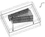
도 2는 광대역 인덕터의 3D 렌더링을 도시한다.
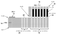
도 3은 본 발명의 광대역 필터의 개략도를 도시한다.
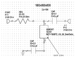
도 4는 새로운 광대역 인덕터를 사용하는 광대역 필터에 대한 전기 회로를 도시한다.
도 5는 새로운 광대역 인덕터를 사용하여 광대역 필터에 대한 전기 회로의 시뮬레이션을 도시한다.
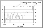
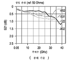
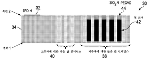
도 6은 바이어스T 회로에서 코일크래프트(Coilcraft)에 의해 만들어진 광대역 인덕터의 삽입 손실을 도시한다.도 7은 BBI의 단일 웨이퍼 구현을 도시한다.
비록 본 발명의 실시예들이 첨부 도면들을 참조하여 완전히 설명되었지만, 다양한 변화들 및 수정들이 통상의 기술자들에게 명백해짐이 유의되어야 한다. 이러한 변화들 및 수정들은 첨부된 청구범위에서 정의된 바와 같이 본 발명의 실시예들의 범위 내에 포함되는 것으로 이해되어야 한다.
| 단계 1 | 포토디파이너블 유리(PDG: photodefinable glass) 기판(14)의 측면 1은 포토레지스트로 코팅되고, 여기서 이어서 비아(원형) 패턴은 표준 포토리소그래피 프로세스들을 사용하여 생성된다. 원형 비아 패턴은 측면 1에서 구리 패턴(22)의 단부와 정렬된다. 비아 간격이 10μm 내지 250μm(예를 들어 50μm) 범위일 수 있는 경우, 직경이 5μm 내지 200μm(예를 들어 25μm)이고 비아 깊이가 25μm 내지 1000μm(예를 들어 300μm)인 중심 대 중심 간격. |
| 단계 2 | 이어서, 원형 비아 패턴(도 2 참조)은 적어도 2 J/cm2의 310 nm 광에 노출된다. 이어서, 포토레지스트는 표준 스트리퍼(stripper)로 제거된다. |
| 단계 3 | 이어서, PDG 기판은 UV 노출 섹션을 세라믹 상으로 변환하기 위해 적어도 10분 동안 600℃로 베이킹된다. |
| 단계 4 | 이어서, 세라믹 상은 10% HF 용액으로 화학적 에칭을 사용하여 측면 1의 구리 도금 영역까지 제거된다. |
| 단계 5 | 이어서, PDG 기판 1은 전기도금조에 배치되고 여기서 비아들은 구리로 채워진다. |
| 단계 6 | PDG(photodefinable glass) 기판 1(도 3 기판(14))의 측면 1 표면에 티타늄 접착 층을 증착한 다음 구리(Cu)의 얇은 층을 증착한다. |
| 단계 7 | 티타늄(Ti)은 스퍼터링, e-빔 증발 PLD 및/또는 CVD를 포함하지만 이에 제한되지 않는 다수의 기법들에 의해 증착될 수 있다. Ti 층의 두께는 5 nm 내지 200 nm, 예를 들어 100 nm의 범위일 수 있다. Cu 층의 두께는 200nm 내지 1,000nm, 예를 들어 500nm 범위일 수 있다. |
| 단계 8 | Ti 및 Cu의 박막은 표준 포토레지스트 코팅, 노출 및 현상액 또는 아르곤 이온 밀 프로세스들을 사용하여 에칭될 수 있다. |
| 단계 9 | 이어서, 포토레지스트는 기존의 포토레지스트 스트리퍼를 사용하여 제거된다. PDG 기판 1(도 3의 기판(14))은 전기도금 시스템에 배치되고, 여기서 구리는 Ti/Cu 층에 도금된다. |
| 단계 10 | 이어서, 땜납 볼(24)은 구리 충전 비아 각각에 적용된다. 땜납 볼은 광대역 인덕터의 저주파 부분(18)에 있는 기판 1(도 3의 기판(14))의 측면 2에 배치된다. 땜납은 PDG 기판 1(도 3의 기판(14))과 2(도 3의 기판(16)) 사이에서 전기적, 기계적, 또는 전기적 및 기계적 연결 둘 모두로서 작용한다. 대안적으로, 땜납 볼(24)은 기판 2(도 3의 기판(16))의 측면 3에 적용될 수 있다. |
| 단계 11 | PDG 기판 2의 측면 3(도 3의 기판(16))은 포토레지스트로 코팅되고, 이어서 비아(원형) 패턴은 표준 포토리소그래피 프로세스들을 사용하여 생성된다. |
| 단계 12 | 이어서 원형 비아 패턴은 적어도 10분 동안 적어도 2 J/cm2의 310nm 광에 노출된다. 이어서, 포토레지스트는 표준 스트리퍼로 제거된다. |
| 단계 13 | 이어서, PDG 기판 2의 측면 3(도 3의 기판(16))은 포토레지스트로 코팅되고, 여기서 이어서 직사각형 패턴은 표준 포토리소그래피 프로세스들을 사용하여 생성된다. |
| 단계 14 | 이어서, 직사각형 패턴은 적어도 8분 동안 적어도 2 J/cm2의 310nm 광에 노출된다. 이어서, 포토레지스트는 표준 스트리퍼로 제거된다. |
| 단계 15 | PDG 기판 2(도 3의 기판(16))는 UV 노출 섹션을 세라믹 상으로 변환하기 위해 적어도 10분 동안 600℃로 베이킹된다. |
| 단계 16 | 이어서, 비아의 세라믹 상은 10% HF 용액으로 화학적 에칭을 사용하여 측면 4의 구리 도금 영역까지 선택적으로 제거된다. |
| 단계 17 | PDG 기판 2(도 3의 기판(16))는 전기도금조에 배치되고, 여기서 비아들은 구리로 채워진다. |
| 단계 18 | 이어서, 직사각형의 세라믹 상은 10% HF 용액을 사용한 화학적 에칭을 사용하여 25um 내지 500um, 예를 들어 300um까지 선택적으로 제거되어 공동을 형성한다. |
| 단계 19 | 이어서, 직사각형 개구는 실크-스크리닝 기법을 사용하여 상업적으로 입수가능한 페라이트 페이스트로 채워지고 제조업체에 의해 규정된 대로 어닐링된다. |
| 단계 20 | 티타늄(Ti) 및 구리(Cu)는 스퍼터링, e-빔 증발 PLD 및/또는 CVD를 포함하지만 이에 제한되지 않는 다수의 상이한 기법들에 의해 PDG 기판 2 측면 4(도 3의 기판(16)) 상에 증착될 수 있다. Ti 층의 두께는 5 nm 내지 200 nm, 예를 들어 100 nm의 범위일 수 있다. Cu 층의 두께는 200nm 내지 1,000nm, 예를 들어 500nm의 범위일 수 있다. |
| 단계 21 | Ti/Cu의 박막은 표준 포토레지스트 코팅, 노출 및 현상 프로세스를 사용하여 패턴화 에칭되고, 이어서 구리 도금을 위한 패턴화된 접착 층을 생성하기 위해 아르곤 이온 밀링된다. 이어서, 포토레지스트는 기존의 포토레지스트 스트리퍼를 사용하여 제거된다. |
| 단계 22 | PDG 기판 2(도 3의 기판(16))은 전기도금 시스템에 배치되고, 여기서 구리는 Ti/Cu 층에 도금된다. |
| 단계 23 | 이어서, PDG 기판 2(도 3 기판(16))은 개별 다이로 다이싱된다. |
| 단계 24 | 이어서, 다이는 PDG 기판 1(도 3 기판(16)) 땜납 범프들(24)에 추가되고 땜납은 리플로우되어, 기판 1(도 3의 기판(14) 및 기판 2(도 3의 기판(16))을 함께 본딩한다. |
| 단계 25 | 회로를 완성하기 위해, 집적된 수동 디바이스(IPD: integrated passive device) 커패시터와 같은 커패시터(12)는 또한 PDG 기판 1(도 3의 기판(14))에 추가된다. |
| 단계 1 | PDG 기판 1(도 7의 기판(34))의 측면 1은 포토레지스트로 코팅되고, 이어서 여기서 비아(원형) 패턴은 표준 포토리소그래피 프로세스들을 사용하여 생성된다. 원형 비아 패턴은 측면 1에서 구리 패턴의 단부와 정렬된다. 비아 간격이 10μm 내지 250μm(예를 들어 50μm) 범위일 수 있는 경우, 직경이 5μm 내지 200μm(예를 들어 25μm)이고 비아 깊이가 25μm 내지 1000μm(예를 들어 300μm)인 중심 대 중심 간격. |
| 단계 2 | 이어서 원형 비아 패턴은 적어도 10분 동안 적어도 2 J/cm2의 310nm 광에 노출된다. 이어서, 포토레지스트는 표준 스트리퍼로 제거된다. |
| 단계 3 | 이어서, PDG 기판 1의 측면 2(도 7의 기판(34))은 포토레지스트로 코팅되고 여기서 이어서 직사각형 패턴은 표준 포토리소그래피 프로세스를 사용하여 생성된다. |
| 단계 4 | 이어서, 직사각형 패턴은 적어도 8분 동안 적어도 2 J/cm2의 310nm 광에 노출된다. 이어서, 포토레지스트는 표준 스트리퍼로 제거된다. |
| 단계 5 | 이어서, PDG 기판 1(도 7의 기판(34))는 UV 노출 섹션을 세라믹 상으로 변환하기 위해 적어도 10분 동안 600℃로 베이킹된다. |
| 단계 6 | 이어서, 비아들의 세라믹 상 및 페라이트 재료에 대한 직사각형 공동은 10% HF 용액으로 화학적 에칭을 사용하여, 측면 2의 구리 도금 영역까지 선택적으로 제거된다. |
| 단계 7 | 이어서, PDG 기판 1(도 7의 기판(34))는 전기도금조에 배치되고, 여기서 비아들은 구리로 채워진다. |
| 단계 8 | 이어서, 직사각형의 세라믹 상은 10% HF 용액을 사용한 화학적 에칭을 사용하여 25um 내지 500um, 바람직하게 300um까지 선택적으로 제거되어 공동을 형성한다. |
| 단계 9 | 이어서, 직사각형 개구는 실크-스크리닝 기법을 사용하여 상업적으로 입수가능한 페라이트 페이스트로 채워지고 제조업체에 의해 규정된 대로 어닐링된다. |
| 단계 10 | 티타늄(Ti) 및 구리(Cu)는 스퍼터링, e-빔 증발 PLD 및/또는 CVD를 포함하지만 이에 제한되지 않는 다수의 상이한 기법들에 의해 PDG 기판 1(도 7의 기판(34)) 측면 1 상에 증착될 수 있다. Ti 층의 두께는 5 nm 내지 200 nm, 바람직하게는 100nm의 범위일 수 있다. Cu 층의 두께는 200nm 내지 1,000nm, 예를 들어 500nm 범위일 수 있다. |
| 단계 11 | Ti/Cu의 박막은 표준 포토레지스트 코팅, 노출 및 현상 프로세스를 사용하여 패턴화 에칭되고, 이어서 구리 도금을 위한 패턴화된 접착 층을 생성하기 위해 아르곤 이온 밀링된다. 이어서, 포토레지스트는 기존의 포토레지스트 스트리퍼를 사용하여 제거된다. |
| 단계 12 | 이어서, PDG 기판 1(도 7의 기판(34))은 전기도금 시스템에 배치되고, 여기서 구리는 Ti/Cu 층에 도금된다. |
| 단계 13 | PDG 기판 1(도 7의 기판(34))은 PECVD 시스템 또는 다른 시스템을 사용하여 패시베이션 층(44)(예를 들어, SiO2)으로 코팅된다. |
| 단계 14 | PDG 기판 1(도 7의 기판(34)) 측면 2 상에, SiO2는 CMP 래핑되고 평평하게 폴리싱된다. |
| 단계 15 | PDG 기판 1(도 7, 기판(34)) 측면 2 상에, 포토레지스트가 적용되고, 노출되고, 비아 패턴을 노출시키기 위해 현상된다. |
| 단계 16 | 이어서, SiO2 비아 패턴은 인덕터 구조를 완성하는 경로를 클리어하기 위해 구리로 채워진 비아까지 플라즈마 에칭된다. |
| 단계 17 | 티타늄(Ti) 및 구리(Cu)는 스퍼터링, e-빔 증발 PLD 및/또는 CVD를 포함하지만 이에 제한되지 않는 다수의 상이한 기법들에 의해 PDG 기판 1(도 7의 기판(34)) 측면 2 상에 증착될 수 있다. Ti 층의 두께는 5 nm 내지 200 nm, 바람직하게는 100nm의 범위일 수 있다. Cu 층의 두께는 200nm 내지 1,000nm, 예를 들어 500nm 범위일 수 있다. |
| 단계 18 | Ti/Cu의 박막은 표준 포토레지스트 코팅, 노출 및 현상 프로세스를 사용하여 패턴화 에칭되고, 이어서 구리 도금을 위한 패턴화된 접착 층을 생성하기 위해 아르곤 이온 밀링된다. 이어서, 포토레지스트는 기존의 포토레지스트 스트리퍼를 사용하여 제거된다. |
| 단계 19 | 이어서, PDG 기판 1(도 7의 기판(34))은 전기도금 시스템에 배치되고, 여기서 구리는 Ti/Cu 층에 도금된다. |
| 단계 20 | 회로를 완성하기 위해 IPD 커패시터는 PDG 기판 1 기판(도 7의 기판(34)) 상에 추가된다. |
| 단계 21 | 이어서, PDG 기판 1(도 7의 기판(34))은 개별 다이로 다이싱된다. |
Claims (38)
- 광대역 인덕터를 생성하는 방법에 있어서,
원뿔형 인덕터의 기판의 제1 측에 제1 트렌치들을 형성하고 전도성 재료로 상기 트렌치들을 채우는 단계;
각각의 상기 제1 트렌치들의 제1 단부 및 제2 단부에 각각 연결되는 상기 기판을 통해 제1 및 제2 비아들을 형성하고 전도성 재료로 상기 제1 및 제2 비아들을 채우는 단계; 및
상기 제1 측에 대향하는 상기 기판의 제2 측에 제2 트렌치를 형성하고, 상기 제2 트렌치들을 전도성 재료로 채우는 단계로서, 제1 및 제2 비아에 연결되는 상기 제2 트렌치들 각각은 원뿔 형상이고, 상기 제1 및 제2 트렌치들은 광대역 인덕터인, 방법. - 제 1 항에 있어서, 상기 기판은 감광성 유리 기판이고, 상기 제1 또는 제2 측에 트렌치들을 형성하는 단계는,
상기 기판 상에 트렌치 패턴을 갖는 포토레지스트를 형성하는 단계;
상기 감광성 유리 기판의 적어도 일부를 활성화 에너지 소스에 노출시키는 단계;
상기 감광성 유리 기판을 유리 전이 온도보다 높게 적어도 10분 동안 가열하는 단계;
상기 감광성 유리 기판을 냉각시켜 상기 노출된 유리의 적어도 일부를 결정질 재료로 변형시켜 유리-결정질 기판을 형성하는 단계;
에천트로 상기 유리-결정질 기판 트렌치들을 에칭하는 단계;
상기 감광성 유리 기판의 에칭된 트렌치들 외부 영역을 활성화 에너지 소스에 플러드 노출(flood exposing)시키는 단계;
상기 감광성 유리 기판을 유리 전이 온도보다 높게 적어도 10분 동안 가열하는 단계;
감광성 유리/세라믹 기판을 냉각시켜 상기 노출된 유리를 결정질 재료로 변환시켜 유리-결정질 기판을 형성하는 단계; 및
전도성 재료 접지면으로 상기 트렌치들을 선택적으로 채우고 하나 이상의 금속들로 입력 및 출력 채널들을 선택적으로 채우는 단계를 포함하고, 상기 금속은 회로에 연결되는, 방법. - 제 1 항에 있어서, 상기 기판은 감광성 유리 기판이고, 상기 제1 측에서 상기 제2 측으로 비아들을 형성하는 단계는:
상기 기판 상에 비아 패턴을 갖는 포토레지스트를 형성하는 단계;
상기 감광성 유리 기판의 적어도 일부를 활성화 에너지 소스에 노출시키는 단계;
상기 감광성 유리 기판을 유리 전이 온도보다 높게 적어도 10분 동안 가열하는 단계;
상기 감광성 유리 기판을 냉각시켜 상기 노출된 유리의 적어도 일부를 결정질 재료로 변형시켜 유리-결정질 기판을 형성하는 단계;
에천트로 상기 유리-결정질 기판 비아들을 에칭하는 단계;
상기 감광성 유리 기판의 에칭된 비아들 외부 영역을 활성화 에너지 소스에 플러드 노출시키는 단계;
상기 감광성 유리 기판을 유리 전이 온도보다 높게 적어도 10분 동안 가열하는 단계;
감광성 유리/세라믹 기판을 냉각시켜 상기 노출된 유리를 결정질 재료로 변환시켜 유리-결정질 기판을 형성하는 단계; 및
상기 비아들을 전도성 재료로 선택적으로 채우는 단계를 포함하는, 방법. - 제 1 항에 있어서, 상기 기판은 포토디파이너블 유리(photodefinable glass)인, 방법.
- 제 1 항에 있어서, 상기 비아 및 트렌치 간격은 10 ㎛ 내지 250 ㎛, 바람직하게는 50 ㎛인, 방법.
- 제 1 항에 있어서, 상기 비아 직경은 5 ㎛ 내지 200 ㎛, 바람직하게는 25 ㎛인, 방법.
- 제 1 항에 있어서, 상기 비아 및 트렌치 높이는 25 ㎛ 내지 1000㎛, 바람직하게는 300 ㎛인, 방법.
- 제 1 항에 있어서, 상기 광대역 인덕터는 고주파 및 저주파 섹션을 포함하는, 방법.
- 제 1 항에 있어서, 상기 광대역 인덕터는 2개의 반도체 기판들로 구성되는, 방법.
- 제 1 항에 있어서, 상기 광대역 인덕터는 하나의 반도체 기판으로 구성되는, 방법.
- 제 1 항에 있어서, 상기 광대역 인덕터는 직사각형이 아닌, 방법.
- 제 1 항에 있어서, 상기 광대역 인덕터는 페라이트 재료로 채워진 공동을 포함하는, 방법.
- 제 1 항에 있어서, 상기 광대역 인덕터는 회로를 형성하는 저항기들, 커넥터들 또는 커패시터들로부터 선택된 하나 이상의 전기 구성요소들을 더 포함하는, 방법.
- 제 1 항에 있어서, 상기 광대역 인덕터는 회로 기판에 본딩되는, 방법.
- 광대역 인덕터를 생성하는 방법에 있어서,
제1 트렌치들 각각의 제1 단부 및 제2 단부에 각각 연결되는 감광성 유리 기판을 통해 제1 및 제2 비아들을 형성하고 전도성 재료로 상기 제1 및 제2 비아들을 채움으로써, 원뿔형 인덕터의 상기 감광성 유리 기판의 제1 측 상에 상기 제1 트렌치들을 형성하고 전도성 재료로 상기 트렌치들을 채우는 단계; 및
제1 측에 대향하는 상기 감광성 유리 기판의 제2 측에 제2 트렌치들을 형성하고, 상기 제2 트렌치들을 전도성 재료로 채우는 단계를 포함하고, 상기 제1 및 제2 비아에 연결되는 상기 제2 트렌치들 각각은 원뿔 형상이고, 상기 제1 및 제2 트렌치들은 광대역 인덕터인, 방법. - 제 15 항에 있어서, 상기 제1 또는 제2 측에 트렌치들을 형성하는 단계는,
상기 기판 상에 트렌치 패턴을 갖는 포토레지스트를 형성하는 단계;
상기 감광성 유리 기판의 적어도 일부를 활성화 에너지 소스에 노출시키는 단계;
상기 감광성 유리 기판을 유리 전이 온도보다 높게 적어도 10분 동안 가열하는 단계;
상기 감광성 유리 기판을 냉각시켜 상기 노출된 유리의 적어도 일부를 결정질 재료로 변형시켜 유리-결정질 기판을 형성하는 단계;
에천트로 상기 유리-결정질 기판 트렌치들을 에칭하는 단계;
상기 감광성 유리 기판의 에칭된 트렌치들 외부 영역을 활성화 에너지 소스에 플러드 노출시키는 단계;
상기 감광성 유리 기판을 유리 전이 온도보다 높게 적어도 10분 동안 가열하는 단계;
감광성 유리/세라믹 기판을 냉각시켜 상기 노출된 유리를 결정질 재료로 변환시켜 유리-결정질 기판을 형성하는 단계; 및
전도성 재료 접지면으로 상기 트렌치들을 선택적으로 채우고 하나 이상의 금속들로 입력 및 출력 채널들을 선택적으로 채우는 단계를 포함하고, 상기 금속은 회로에 연결되는, 방법. - 제 15 항에 있어서, 상기 제1 측에서 상기 제2 측으로 비아들을 형성하는 단계는:
상기 기판 상에 비아 패턴을 갖는 포토레지스트를 형성하는 단계;
상기 감광성 유리 기판의 적어도 일부를 활성화 에너지 소스에 노출시키는 단계;
상기 감광성 유리 기판을 유리 전이 온도보다 높게 적어도 10분 동안 가열하는 단계;
상기 감광성 유리 기판을 냉각시켜 상기 노출된 유리의 적어도 일부를 결정질 재료로 변형시켜 유리-결정질 기판을 형성하는 단계;
에천트로 상기 유리-결정질 기판 비아들을 에칭하는 단계;
상기 감광성 유리 기판의 에칭된 비아들 외부 영역을 활성화 에너지 소스에 플러드 노출시키는 단계;
상기 감광성 유리 기판을 유리 전이 온도보다 높게 적어도 10분 동안 가열하는 단계;
감광성 유리/세라믹 기판을 냉각시켜 상기 노출된 유리를 결정질 재료로 변환시켜 유리-결정질 기판을 형성하는 단계; 및
상기 비아들을 전도성 재료로 선택적으로 채우는 단계를 포함하는, 방법. - 제 15 항에 있어서, 상기 비아 및 트렌치 간격은 10 ㎛ 내지 250 ㎛, 바람직하게는 50 ㎛인, 방법.
- 제 15 항에 있어서, 상기 비아 직경은 5 ㎛ 내지 200 ㎛, 바람직하게는 25 ㎛인, 방법.
- 제 15 항에 있어서, 상기 비아, 상기 트렌치, 또는 둘 모두는 25 ㎛ 내지 1000 ㎛, 바람직하게는 300 ㎛의 높이를 갖는, 방법.
- 제 15 항에 있어서, 상기 광대역 인덕터는 고주파 및 저주파 섹션을 포함하는, 방법.
- 제 15 항에 있어서, 상기 광대역 인덕터는 2개의 반도체 기판으로 구성되는, 방법.
- 제 15 항에 있어서, 상기 광대역 인덕터는 하나의 반도체 기판으로 구성되는, 방법.
- 제 15 항에 있어서, 상기 광대역 인덕터는 직사각형이 아닌, 방법.
- 제 15 항에 있어서, 상기 광대역 인덕터는 페라이트 재료로 채워진 공동을 포함하는, 방법.
- 제 15 항에 있어서, 상기 광대역 인덕터는 회로를 형성하는 저항기들, 커넥터들 또는 커패시터들로부터 선택된 하나 이상의 전기 구성요소들을 더 포함하는, 방법.
- 제 15 항에 있어서, 상기 광대역 인덕터는 회로 기판에 본딩되는, 방법.
- 광대역 인덕터에 있어서,
원뿔형 인덕터의 기판의 제1 측 상의 제1 트렌치들로서, 상기 트렌치들은 전도성 재료로 채워지는, 상기 제1 트렌치;
각각의 제1 트렌치들의 제1 단부 및 제2 단부에 각각 연결되는 상기 기판을 통한 제1 및 제2 비아들로서, 상기 제1 및 제2 비아들은 전도성 재료로 채워지는, 상기 제1 및 제2 비아; 및
상기 제1 측에 대향하는 상기 기판의 제2 측 상의 제2 트렌치들로서, 상기 제2 트렌치들은 전도성 재료로 채워지는, 상기 제2 트렌치들을 포함하고, 상기 제1 및 제2 비아에 연결되는 상기 제2 트렌치들의 각각은 원뿔 형상이고, 상기 제1 및 제2 트렌치들은 광대역 인덕터인, 광대역 인덕터. - 제 28 항에 있어서, 상기 기판은 감광성 유리 기판인, 광대역 인덕터.
- 제 28 항에 있어서, 상기 비아 및 트렌치 간격은 10 ㎛ 내지 250 ㎛, 바람직하게는 50 ㎛인, 광대역 인덕터.
- 제 28 항에 있어서, 상기 비아 직경은 5 ㎛ 내지 200 ㎛, 바람직하게는 25 ㎛인, 광대역 인덕터.
- 제 28 항에 있어서, 상기 비아, 상기 트렌치, 또는 둘 모두는 25 ㎛ 내지 1000 ㎛, 바람직하게는 300 ㎛의 높이를 갖는, 광대역 인덕터.
- 제 28 항에 있어서, 상기 광대역 인덕터는 고주파 및 저주파 섹션을 포함하는, 광대역 인덕터.
- 제 28 항에 있어서, 상기 광대역 인덕터는 2개의 반도체 기판으로 구성되는, 광대역 인덕터.
- 제 28 항에 있어서, 상기 광대역 인덕터는 하나의 반도체 기판으로 구성되는, 광대역 인덕터.
- 제 28 항에 있어서, 상기 광대역 인덕터는 직사각형이 아닌, 광대역 인덕터.
- 제 28 항에 있어서, 상기 광대역 인덕터는 페라이트 재료로 채워진 공동을 포함하는, 광대역 인덕터.
- 제 28 항에 있어서, 상기 광대역 인덕터는 회로를 형성하는 저항기들, 커넥터들 또는 커패시터들로부터 선택된 하나 이상의 전기 구성요소들을 더 포함하는, 광대역 인덕터.
Applications Claiming Priority (3)
| Application Number | Priority Date | Filing Date | Title |
|---|---|---|---|
| US202063011505P | 2020-04-17 | 2020-04-17 | |
| US63/011,505 | 2020-04-17 | ||
| PCT/US2021/027499 WO2021211855A1 (en) | 2020-04-17 | 2021-04-15 | Broadband inductor |
Publications (1)
| Publication Number | Publication Date |
|---|---|
| KR20220164800A true KR20220164800A (ko) | 2022-12-13 |
Family
ID=78085203
Family Applications (1)
| Application Number | Title | Priority Date | Filing Date |
|---|---|---|---|
| KR1020227040090A Ceased KR20220164800A (ko) | 2020-04-17 | 2021-04-15 | 광대역 인덕터 |
Country Status (6)
| Country | Link |
|---|---|
| US (1) | US11908617B2 (ko) |
| EP (1) | EP4121988A4 (ko) |
| JP (1) | JP2023516817A (ko) |
| KR (1) | KR20220164800A (ko) |
| CA (1) | CA3177603C (ko) |
| WO (1) | WO2021211855A1 (ko) |
Families Citing this family (2)
| Publication number | Priority date | Publication date | Assignee | Title |
|---|---|---|---|---|
| JP7514228B2 (ja) | 2018-07-13 | 2024-07-10 | ノールズ カゼノビア インコーポレイテッド | ミリ波フィルタアレイ |
| US20240347446A1 (en) * | 2023-04-14 | 2024-10-17 | Infineon Technologies Ag | Lateral coils used for energy transfer over isolation region in multi-voltage devices |
Family Cites Families (315)
| Publication number | Priority date | Publication date | Assignee | Title |
|---|---|---|---|---|
| FR957663A (ko) | 1943-12-08 | 1950-02-23 | ||
| GB619779A (en) | 1946-01-18 | 1949-03-15 | Gen Aniline & Film Corp | Improvements in iron powder and cores produced therefrom |
| BE478714A (ko) | 1946-09-09 | |||
| US2515941A (en) | 1946-09-09 | 1950-07-18 | Corning Glass Works | Photosensitive opal glass |
| BE493137A (ko) | 1949-01-07 | |||
| US2628160A (en) | 1951-08-30 | 1953-02-10 | Corning Glass Works | Sculpturing glass |
| BE513836A (ko) | 1951-08-30 | |||
| US2971853A (en) | 1953-03-05 | 1961-02-14 | Corning Glass Works | Ceramic body and method of making it |
| US3281264A (en) | 1963-01-31 | 1966-10-25 | Coast Metals Inc | Method of gold-plating aluminum |
| US3292115A (en) | 1964-09-11 | 1966-12-13 | Hazeltine Research Inc | Easily fabricated waveguide structures |
| JPS5321827B2 (ko) | 1973-02-12 | 1978-07-05 | ||
| GB1407151A (en) | 1973-02-13 | 1975-09-24 | Okikiolu G O | System assemblies of energized components having tapering form for developing progressively increasing electromagnetic energy fields |
| US3993401A (en) | 1975-02-10 | 1976-11-23 | Minnesota Mining And Manufacturing Company | Retroreflective material including geometric fresnel zone plates |
| US3985531A (en) | 1975-03-19 | 1976-10-12 | Corning Glass Works | Spontaneously-formed fluormica glass-ceramics |
| US4029605A (en) | 1975-12-08 | 1977-06-14 | Hercules Incorporated | Metallizing compositions |
| US4131516A (en) | 1977-07-21 | 1978-12-26 | International Business Machines Corporation | Method of making metal filled via holes in ceramic circuit boards |
| US4413061A (en) | 1978-02-06 | 1983-11-01 | International Business Machines Corporation | Glass-ceramic structures and sintered multilayer substrates thereof with circuit patterns of gold, silver or copper |
| JPS56155587A (en) | 1980-05-02 | 1981-12-01 | Fujitsu Ltd | Printed circuit board |
| JPS57200042A (en) | 1981-06-02 | 1982-12-08 | Hoya Corp | Exposure method for chemically machinable photosensitive glass |
| US4537612A (en) | 1982-04-01 | 1985-08-27 | Corning Glass Works | Colored photochromic glasses and method |
| JPS5939949U (ja) | 1982-09-08 | 1984-03-14 | アルプス電気株式会社 | 高周波回路装置 |
| US4647940A (en) | 1982-09-27 | 1987-03-03 | Rogers Corporation | Parallel plate waveguide antenna |
| US5078771A (en) | 1989-02-07 | 1992-01-07 | Canyon Materials, Inc. | Method of making high energy beam sensitive glasses |
| US4514053A (en) | 1983-08-04 | 1985-04-30 | Corning Glass Works | Integral photosensitive optical device and method |
| JPS61149905A (ja) | 1984-12-25 | 1986-07-08 | Fujitsu Ltd | 光合分波器 |
| JPS61231529A (ja) | 1985-04-08 | 1986-10-15 | Agency Of Ind Science & Technol | 光制御型光スイツチ装置 |
| JPS62202840A (ja) | 1986-03-03 | 1987-09-07 | Toshiba Corp | 感光性ガラスの加工方法 |
| US4692015A (en) | 1986-03-14 | 1987-09-08 | Xerox Corporation | Short focal lens array with multi-magnification properties |
| JPS63128699A (ja) | 1986-11-19 | 1988-06-01 | 株式会社日立製作所 | 感光性ガラス−セラミツク多層配線基板 |
| CA1320507C (en) | 1987-10-07 | 1993-07-20 | Elizabeth A. Boylan | Thermal writing on glass or glass-ceramic substrates and copper-exuding glasses |
| US4788165A (en) | 1987-10-07 | 1988-11-29 | Corning Glass Works | Copper-exuding, boroaluminosilicate glasses |
| US4942076A (en) | 1988-11-03 | 1990-07-17 | Micro Substrates, Inc. | Ceramic substrate with metal filled via holes for hybrid microcircuits and method of making the same |
| JP2737292B2 (ja) | 1989-09-01 | 1998-04-08 | 富士通株式会社 | 銅ペースト及びそれを用いたメタライズ方法 |
| US5147740A (en) | 1990-08-09 | 1992-09-15 | Rockwell International Corporation | Structure and process for fabricating conductive patterns having sub-half micron dimensions |
| US5215610A (en) | 1991-04-04 | 1993-06-01 | International Business Machines Corporation | Method for fabricating superconductor packages |
| BE1004844A7 (fr) | 1991-04-12 | 1993-02-09 | Laude Lucien Diego | Methodes de metallisation de surfaces a l'aide de poudres metalliques. |
| US5212120A (en) | 1991-06-10 | 1993-05-18 | Corning Incorporated | Photosensitive glass |
| US5395498A (en) | 1991-11-06 | 1995-03-07 | Gombinsky; Moshe | Method for separating biological macromolecules and means therfor |
| JPH05139787A (ja) | 1991-11-19 | 1993-06-08 | Seikosha Co Ltd | 感光性ガラスの加工方法 |
| US5374291A (en) | 1991-12-10 | 1994-12-20 | Director-General Of Agency Of Industrial Science And Technology | Method of processing photosensitive glass |
| JPH05206706A (ja) | 1992-01-30 | 1993-08-13 | Reader Denshi Kk | インターデジタル型バンドパスフィルタ |
| US5371466A (en) | 1992-07-29 | 1994-12-06 | The Regents Of The University Of California | MRI RF ground breaker assembly |
| US6258497B1 (en) | 1992-07-29 | 2001-07-10 | International Business Machines Corporation | Precise endpoint detection for etching processes |
| US5312674A (en) | 1992-07-31 | 1994-05-17 | Hughes Aircraft Company | Low-temperature-cofired-ceramic (LTCC) tape structures including cofired ferromagnetic elements, drop-in components and multi-layer transformer |
| US6017681A (en) | 1992-11-09 | 2000-01-25 | Fujitsu Limited | Method of coupling optical parts and method of forming a mirror |
| GB2290171B (en) | 1994-06-03 | 1998-01-21 | Plessey Semiconductors Ltd | Inductor chip device |
| JPH0826767A (ja) | 1994-07-13 | 1996-01-30 | Nippon Glass Kk | ソーダ石灰シリカ系感光性ガラス及びその製造方法 |
| JPH08179155A (ja) | 1994-12-26 | 1996-07-12 | Ricoh Co Ltd | レンズと光ファイバとの結合方法及びレンズ基板の作成方法 |
| JP3438383B2 (ja) | 1995-03-03 | 2003-08-18 | ソニー株式会社 | 研磨方法およびこれに用いる研磨装置 |
| KR100449615B1 (ko) | 1995-03-10 | 2004-12-08 | 메소 스케일 테크놀러지즈, 엘엘시 | 다-배열,다-특이적전기화학발광시험법 |
| US5919607A (en) | 1995-10-26 | 1999-07-06 | Brown University Research Foundation | Photo-encoded selective etching for glass based microtechnology applications |
| US5733370A (en) | 1996-01-16 | 1998-03-31 | Seagate Technology, Inc. | Method of manufacturing a bicrystal cluster magnetic recording medium |
| JPH107435A (ja) | 1996-06-26 | 1998-01-13 | Ngk Spark Plug Co Ltd | ガラスセラミック配線基板およびその製造方法 |
| EP2159814B1 (en) | 1996-09-26 | 2011-11-09 | Asahi Glass Company, Limited | Protective plate for a plasma display |
| US6562523B1 (en) | 1996-10-31 | 2003-05-13 | Canyon Materials, Inc. | Direct write all-glass photomask blanks |
| JPH10199728A (ja) | 1997-01-07 | 1998-07-31 | Murata Mfg Co Ltd | 薄膜型コイル部品及びその製造方法 |
| US5850623A (en) | 1997-03-14 | 1998-12-15 | Eastman Chemical Company | Method for standardizing raman spectrometers to obtain stable and transferable calibrations |
| JP2000512810A (ja) | 1997-04-25 | 2000-09-26 | コーニンクレッカ フィリップス エレクトロニクス エヌ ヴィ | 封入型多層コンデンサを製造する方法及び封入型多層コンデンサ |
| US5998224A (en) | 1997-05-16 | 1999-12-07 | Abbott Laboratories | Magnetically assisted binding assays utilizing a magnetically responsive reagent |
| US6287965B1 (en) | 1997-07-28 | 2001-09-11 | Samsung Electronics Co, Ltd. | Method of forming metal layer using atomic layer deposition and semiconductor device having the metal layer as barrier metal layer or upper or lower electrode of capacitor |
| US6417754B1 (en) | 1997-12-08 | 2002-07-09 | The Regents Of The University Of California | Three-dimensional coil inductor |
| JPH11176815A (ja) | 1997-12-15 | 1999-07-02 | Ricoh Co Ltd | ドライエッチングの終点判定方法およびドライエッチング装置 |
| US6598291B2 (en) | 1998-03-20 | 2003-07-29 | Viasystems, Inc. | Via connector and method of making same |
| US6115521A (en) | 1998-05-07 | 2000-09-05 | Trw Inc. | Fiber/waveguide-mirror-lens alignment device |
| US6171886B1 (en) | 1998-06-30 | 2001-01-09 | Eastman Kodak Company | Method of making integrated hybrid silicon-based micro-actuator devices |
| US6046641A (en) | 1998-07-22 | 2000-04-04 | Eni Technologies, Inc. | Parallel HV MOSFET high power stable amplifier |
| JP2000114818A (ja) | 1998-10-07 | 2000-04-21 | Hitachi Metals Ltd | 集中定数型非可逆回路素子 |
| JP2000199827A (ja) | 1998-10-27 | 2000-07-18 | Sony Corp | 光導波装置およびその製造方法 |
| US6136210A (en) | 1998-11-02 | 2000-10-24 | Xerox Corporation | Photoetching of acoustic lenses for acoustic ink printing |
| JP2000228615A (ja) | 1999-02-05 | 2000-08-15 | Tokin Corp | Lcバンドパスフィルタ |
| JP3360065B2 (ja) | 1999-03-24 | 2002-12-24 | エルジー電子株式会社 | 感光性ガラス基板を利用したマイクロ構造物の製造方法 |
| AUPQ056099A0 (en) * | 1999-05-25 | 1999-06-17 | Silverbrook Research Pty Ltd | A method and apparatus (pprint01) |
| JP3756041B2 (ja) | 1999-05-27 | 2006-03-15 | Hoya株式会社 | 多層プリント配線板の製造方法 |
| US6485690B1 (en) | 1999-05-27 | 2002-11-26 | Orchid Biosciences, Inc. | Multiple fluid sample processor and system |
| FR2795745B1 (fr) | 1999-06-30 | 2001-08-03 | Saint Gobain Vitrage | Procede de depot d'une couche a base de tungstene et/ou de molybdene sur un substrat verrier, ceramique ou vitroceramique, et substrat ainsi revetu |
| JP2001033664A (ja) | 1999-07-21 | 2001-02-09 | Hitachi Cable Ltd | 光ファイバブロック |
| US6278352B1 (en) | 1999-07-26 | 2001-08-21 | Taiwan Semiconductor Manufacturing Company | High efficiency thin film inductor |
| US7179638B2 (en) | 1999-07-30 | 2007-02-20 | Large Scale Biology Corporation | Microarrays and their manufacture by slicing |
| US6538775B1 (en) | 1999-09-16 | 2003-03-25 | Reveo, Inc. | Holographically-formed polymer dispersed liquid crystals with multiple gratings |
| US6403286B1 (en) | 1999-11-04 | 2002-06-11 | Corning Incorporated | High aspect ratio patterning of glass film |
| US6689824B2 (en) | 2000-02-18 | 2004-02-10 | Rohm And Haas Company | Prepaints and method of preparing road-marking paints from prepaints |
| JP4200631B2 (ja) | 2000-03-29 | 2008-12-24 | 沖電気工業株式会社 | オンチップ・コイルとその製造方法 |
| US6579817B2 (en) | 2000-04-26 | 2003-06-17 | Matsushita Electric Industrial Co., Ltd. | Dielectric ceramic composition and method for producing the same, and device for communication apparatus using the same |
| US6329702B1 (en) | 2000-07-06 | 2001-12-11 | Tyco Electronics Corporation | High frequency carrier |
| US6510264B2 (en) | 2000-07-31 | 2003-01-21 | Corning Incorporated | Bulk internal bragg gratings and optical devices |
| US7829348B2 (en) | 2000-09-22 | 2010-11-09 | Iowa State University Research Foundation, Inc. | Raman-active reagents and the use thereof |
| AU2001296809A1 (en) | 2000-10-10 | 2002-04-22 | Biotrove, Inc. | Apparatus for assay, synthesis and storage, and methods of manufacture, use, and manipulation thereof |
| US7033821B2 (en) | 2000-11-08 | 2006-04-25 | Surface Logix, Inc. | Device for monitoring cell motility in real-time |
| KR100392956B1 (ko) | 2000-12-30 | 2003-07-28 | 엘지전자 주식회사 | 플라즈마 디스플레이 패널의 격벽 제조방법 |
| KR100368930B1 (ko) | 2001-03-29 | 2003-01-24 | 한국과학기술원 | 반도체 기판 위에 높이 떠 있는 3차원 금속 소자, 그 회로모델, 및 그 제조방법 |
| US6932933B2 (en) | 2001-03-30 | 2005-08-23 | The Aerospace Corporation | Ultraviolet method of embedding structures in photocerams |
| US6824974B2 (en) | 2001-06-11 | 2004-11-30 | Genorx, Inc. | Electronic detection of biological molecules using thin layers |
| EP2420824B1 (en) | 2001-06-29 | 2018-11-28 | Meso Scale Technologies LLC | Multi-well plate having an array of wells and kit for use in the conduct of an ECL assay |
| US6771860B2 (en) | 2001-06-29 | 2004-08-03 | Xanoptix, Inc. | Module mounted aligning optical connector |
| CN1630946A (zh) | 2001-07-12 | 2005-06-22 | 株式会社日立制作所 | 电子电路部件 |
| US6843902B1 (en) | 2001-07-20 | 2005-01-18 | The Regents Of The University Of California | Methods for fabricating metal nanowires |
| US20030025227A1 (en) | 2001-08-02 | 2003-02-06 | Zograph, Llc | Reproduction of relief patterns |
| EP1469903A2 (en) | 2001-09-28 | 2004-10-27 | BioValve Technologies, Inc. | Microneedle with membrane |
| KR100814806B1 (ko) | 2001-10-15 | 2008-03-19 | 삼성에스디아이 주식회사 | 스페이서 제조 방법 및 이 스페이서를 갖는 평판 표시 소자 |
| JP2003209411A (ja) | 2001-10-30 | 2003-07-25 | Matsushita Electric Ind Co Ltd | 高周波モジュールおよび高周波モジュールの製造方法 |
| US20040171076A1 (en) | 2001-12-20 | 2004-09-02 | Dejneka Matthew J. | Detectable micro to nano sized structures, methods of manufacture and use |
| US7064103B2 (en) | 2002-01-04 | 2006-06-20 | Becton, Dickinson And Company | Binding protein as biosensors |
| US6867089B2 (en) | 2002-01-28 | 2005-03-15 | Nanya Technology Corporation | Method of forming a bottle-shaped trench in a semiconductor substrate |
| US7470518B2 (en) | 2002-02-12 | 2008-12-30 | Cellectricon Ab | Systems and method for rapidly changing the solution environment around sensors |
| US20030156819A1 (en) | 2002-02-15 | 2003-08-21 | Mark Pruss | Optical waveguide |
| AU2003220148A1 (en) | 2002-03-14 | 2003-09-29 | Corning Incorporated | Fiber array and methods of fabrication |
| WO2003093809A1 (en) | 2002-04-30 | 2003-11-13 | University Of Maryland, Baltimore | Fluorescence sensing |
| JP2003329877A (ja) | 2002-05-14 | 2003-11-19 | Nippon Sheet Glass Co Ltd | 光モジュール |
| US20030231076A1 (en) | 2002-06-03 | 2003-12-18 | Matsushita Electric Industrial Co., Ltd. | Structure of non-reciprocal circuit element |
| US6580054B1 (en) | 2002-06-10 | 2003-06-17 | New Wave Research | Scribing sapphire substrates with a solid state UV laser |
| KR100846383B1 (ko) | 2002-06-29 | 2008-07-15 | 주식회사 하이닉스반도체 | 캐패시터 제조 방법 |
| AU2003266155A1 (en) | 2002-09-11 | 2004-04-30 | Synamem Corporation | Membrane-based assays |
| US6911373B2 (en) | 2002-09-20 | 2005-06-28 | Intel Corporation | Ultra-high capacitance device based on nanostructures |
| US6875544B1 (en) | 2002-10-03 | 2005-04-05 | Sandia Corporation | Method for the fabrication of three-dimensional microstructures by deep X-ray lithography |
| US20040184705A1 (en) | 2003-01-08 | 2004-09-23 | Mikihiro Shimada | Optical waveguide component and method of manufacturing the same |
| US6783920B2 (en) | 2003-01-15 | 2004-08-31 | The Aerospace Corporation | Photosensitive glass variable laser exposure patterning method |
| DE10304606B3 (de) | 2003-02-05 | 2004-06-03 | Magnet-Physik Dr. Steingroever Gmbh | Transformator zur Erzeugung hoher elektrischer Ströme |
| US7601491B2 (en) | 2003-02-06 | 2009-10-13 | Becton, Dickinson And Company | Pretreatment method for extraction of nucleic acid from biological samples and kits therefor |
| US7142086B2 (en) | 2003-02-11 | 2006-11-28 | Oplink Communications, Inc. | Ultra broadband inductor assembly |
| US7150569B2 (en) | 2003-02-24 | 2006-12-19 | Nor Spark Plug Co., Ltd. | Optical device mounted substrate assembly |
| DE602004028349D1 (de) | 2003-03-04 | 2010-09-09 | Rohm & Haas Elect Mat | Koaxiale wellenleitermikrostrukturen und verfahern zu ihrer bildung |
| US20040198582A1 (en) | 2003-04-01 | 2004-10-07 | Borrelli Nicholas F. | Optical elements and methods of making optical elements |
| US6909137B2 (en) | 2003-04-07 | 2005-06-21 | International Business Machines Corporation | Method of creating deep trench capacitor using a P+ metal electrode |
| US7579077B2 (en) | 2003-05-05 | 2009-08-25 | Nanosys, Inc. | Nanofiber surfaces for use in enhanced surface area applications |
| EP1487019A1 (en) | 2003-06-12 | 2004-12-15 | Koninklijke Philips Electronics N.V. | Electronic device and method of manufacturing thereof |
| KR100495219B1 (ko) | 2003-06-25 | 2005-06-14 | 삼성전기주식회사 | Ic칩 내장형 파워 엠프 모듈 |
| WO2005027606A1 (ja) | 2003-09-09 | 2005-03-24 | Hoya Corporation | 両面配線ガラス基板の製造方法 |
| JP4523299B2 (ja) | 2003-10-31 | 2010-08-11 | 学校法人早稲田大学 | 薄膜コンデンサの製造方法 |
| US7335972B2 (en) | 2003-11-13 | 2008-02-26 | Sandia Corporation | Heterogeneously integrated microsystem-on-a-chip |
| US20050170670A1 (en) | 2003-11-17 | 2005-08-04 | King William P. | Patterning of sacrificial materials |
| KR100780610B1 (ko) | 2003-11-28 | 2007-11-29 | 주식회사 하이닉스반도체 | 반도체소자 제조 방법 |
| US6830221B1 (en) | 2003-12-19 | 2004-12-14 | The Aerospace Corporation | Integrated glass ceramic spacecraft |
| US7316063B2 (en) | 2004-01-12 | 2008-01-08 | Micron Technology, Inc. | Methods of fabricating substrates including at least one conductive via |
| JP4153442B2 (ja) | 2004-02-02 | 2008-09-24 | シャープ株式会社 | 光モジュールの製造方法 |
| EP1738378A4 (en) | 2004-03-18 | 2010-05-05 | Nanosys Inc | NANOFIBRE SURFACE BASED CAPACITORS |
| JP4394999B2 (ja) | 2004-04-12 | 2010-01-06 | 大日本印刷株式会社 | 受動素子内蔵配線基板およびその製造方法 |
| CN1262500C (zh) | 2004-04-16 | 2006-07-05 | 武汉理工大学 | 制备纳米孔微晶玻璃/玻璃载体材料的方法 |
| DE102004059252A1 (de) | 2004-06-09 | 2006-01-19 | Schott Ag | Aufbau diffraktiver Optiken durch strukturierte Glasbeschichtung |
| US7176152B2 (en) | 2004-06-09 | 2007-02-13 | Ferro Corporation | Lead-free and cadmium-free conductive copper thick film pastes |
| JP4622359B2 (ja) | 2004-07-22 | 2011-02-02 | コニカミノルタホールディングス株式会社 | インクジェットヘッドの製造方法 |
| US7064045B2 (en) | 2004-08-30 | 2006-06-20 | Miradia Inc. | Laser based method and device for forming spacer structures for packaging optical reflection devices |
| US7132054B1 (en) | 2004-09-08 | 2006-11-07 | Sandia Corporation | Method to fabricate hollow microneedle arrays |
| US7259106B2 (en) | 2004-09-10 | 2007-08-21 | Versatilis Llc | Method of making a microelectronic and/or optoelectronic circuitry sheet |
| US20060147344A1 (en) | 2004-09-30 | 2006-07-06 | The University Of Cincinnati | Fully packed capillary electrophoretic separation microchips with self-assembled silica colloidal particles in microchannels and their preparation methods |
| EP1797617A4 (en) | 2004-10-01 | 2009-08-12 | Rochemont L Pierre De | CERAMIC ANTENNA MODULE AND MANUFACTURING METHOD THEREFOR |
| JP4795677B2 (ja) | 2004-12-02 | 2011-10-19 | ルネサスエレクトロニクス株式会社 | 半導体装置およびそれを用いた半導体モジュール、ならびに半導体装置の製造方法 |
| JP2006179564A (ja) | 2004-12-21 | 2006-07-06 | Nec Corp | 半導体接続基板、半導体装置、半導体デバイス及び半導体基板並びに半導体接続基板の製造方法 |
| DE102005003594B4 (de) | 2004-12-31 | 2016-02-18 | Schott Ag | Verfahren zur Herstellung eines optischen Bauteils, verfahrensgemäß hergestelltes Bauteil sowie derartige Bauteile umfassende Einrichtung |
| US7714688B2 (en) | 2005-01-20 | 2010-05-11 | Avx Corporation | High Q planar inductors and IPD applications |
| KR100682919B1 (ko) | 2005-01-20 | 2007-02-15 | 삼성전자주식회사 | 미세 금속 박막 패턴 형성 방법, 이를 채용한 생체물질고정용 기판 및 바이오칩 |
| US7964380B2 (en) | 2005-01-21 | 2011-06-21 | Argylia Technologies | Nanoparticles for manipulation of biopolymers and methods of thereof |
| KR20060092643A (ko) | 2005-02-18 | 2006-08-23 | 주식회사 하이닉스반도체 | 반도체 메모리 소자 및 그 제조 방법 |
| JP2006236516A (ja) | 2005-02-28 | 2006-09-07 | Hitachi Ltd | 光へッド、光情報再生装置及びその製造方法 |
| JP4020159B2 (ja) | 2005-04-18 | 2007-12-12 | 株式会社村田製作所 | 高周波モジュール |
| JP2006324489A (ja) | 2005-05-19 | 2006-11-30 | Matsushita Electric Ind Co Ltd | チップコイル及びその製造方法 |
| US7355704B2 (en) | 2005-06-13 | 2008-04-08 | Solaris Nanosciences, Inc. | Chemical and biological sensing using metallic particles in amplifying and absorbing media |
| JP2006352750A (ja) | 2005-06-20 | 2006-12-28 | Denso Corp | アンテナコイル、それを用いた共振アンテナ及びカード型無線機 |
| US7755291B2 (en) | 2005-06-27 | 2010-07-13 | Osram Sylvania Inc. | Incandescent lamp that emits infrared light and a method of making the lamp |
| US7247542B2 (en) | 2005-08-10 | 2007-07-24 | Integrated Crystal Technology, Inc. | Fabrication method of spiral inductor on porous glass substrate |
| DE102005039323B4 (de) | 2005-08-19 | 2009-09-03 | Infineon Technologies Ag | Leitbahnanordnung sowie zugehöriges Herstellungsverfahren |
| US7410763B2 (en) | 2005-09-01 | 2008-08-12 | Intel Corporation | Multiplex data collection and analysis in bioanalyte detection |
| JP2006032982A (ja) | 2005-09-02 | 2006-02-02 | Semiconductor Energy Lab Co Ltd | 薄膜の加熱処理方法 |
| US20070080458A1 (en) | 2005-10-11 | 2007-04-12 | Tsuyoshi Ogawa | Hybrid module and method of manufacturing the same |
| TW200721064A (en) | 2005-11-29 | 2007-06-01 | Novatek Microelectronics Corp | Timing controller chip |
| US8003408B2 (en) | 2005-12-29 | 2011-08-23 | Intel Corporation | Modification of metal nanoparticles for improved analyte detection by surface enhanced Raman spectroscopy (SERS) |
| GB2434913A (en) | 2006-02-02 | 2007-08-08 | Xsil Technology Ltd | Support for wafer singulation |
| US7812416B2 (en) | 2006-05-22 | 2010-10-12 | Cardiomems, Inc. | Methods and apparatus having an integrated circuit attached to fused silica |
| JP2007318002A (ja) | 2006-05-29 | 2007-12-06 | Matsushita Electric Ind Co Ltd | 固体撮像装置及びその製造方法 |
| US8192795B2 (en) | 2006-06-28 | 2012-06-05 | Northwestern University | Etching and hole arrays |
| US7990679B2 (en) | 2006-07-14 | 2011-08-02 | Dais Analytic Corporation | Nanoparticle ultracapacitor |
| JP4620643B2 (ja) * | 2006-08-16 | 2011-01-26 | 富士通オプティカルコンポーネンツ株式会社 | インダクタ配線基板、インダクタ配線方法及びバイアスt回路 |
| US8061017B2 (en) | 2006-08-28 | 2011-11-22 | Avago Technologies Ecbu Ip (Singapore) Pte. Ltd. | Methods of making coil transducers |
| JP2008066671A (ja) * | 2006-09-11 | 2008-03-21 | Fuji Electric Device Technology Co Ltd | 薄型磁気部品及びその製造方法 |
| US7965180B2 (en) | 2006-09-28 | 2011-06-21 | Semiconductor Energy Laboratory Co., Ltd. | Wireless sensor device |
| US7847669B2 (en) | 2006-12-06 | 2010-12-07 | Georgia Tech Research Corporation | Micro-electromechanical switched tunable inductor |
| US7556440B2 (en) | 2006-12-22 | 2009-07-07 | Lightwire Inc. | Dual-lensed unitary optical receiver assembly |
| CN101611461B (zh) | 2007-02-14 | 2012-03-21 | 株式会社村田制作所 | 叠层陶瓷电容器及其制造方法 |
| WO2008105496A1 (ja) | 2007-03-01 | 2008-09-04 | Nec Corporation | キャパシタ搭載インターポーザ及びその製造方法 |
| KR100849791B1 (ko) | 2007-03-12 | 2008-07-31 | 삼성전기주식회사 | 캐패시터 내장형 인쇄회로기판 |
| JP2008225339A (ja) | 2007-03-15 | 2008-09-25 | Hitachi Cable Ltd | 光学系接続構造、光学部材及び光伝送モジュール |
| TWI347616B (en) * | 2007-03-22 | 2011-08-21 | Ind Tech Res Inst | Inductor devices |
| JP5104852B2 (ja) | 2007-03-26 | 2012-12-19 | 株式会社村田製作所 | 感光性誘電体ペーストおよびそれを用いた電子部品 |
| US8361333B2 (en) | 2007-03-28 | 2013-01-29 | Life Bioscience, Inc. | Compositions and methods to fabricate a photoactive substrate suitable for shaped glass structures |
| JP4458296B2 (ja) | 2007-03-30 | 2010-04-28 | Tdk株式会社 | 誘電体共振器、誘電体フィルタ及びその特性調整方法 |
| US8143431B2 (en) | 2007-06-05 | 2012-03-27 | Air Products And Chemicals, Inc. | Low temperature thermal conductive inks |
| WO2008154931A1 (en) | 2007-06-18 | 2008-12-24 | Danmarks Tekniske Universitet (Technical University Of Denmark) | Adsorbent beads suitable for use in separation of biological molecules |
| TW200905703A (en) | 2007-07-27 | 2009-02-01 | Delta Electronics Inc | Magnetic device and manufacturing method thereof |
| WO2009029733A2 (en) | 2007-08-28 | 2009-03-05 | Life Biosciences, Inc. | Method of providing a pattern of biological-binding areas for biological testing |
| WO2009062011A1 (en) | 2007-11-07 | 2009-05-14 | Masachusetts Institute Of Technology | Method of forming a locally periodic 3d structure with larger-scale variation in periodic properties and applications thereof |
| JP5133047B2 (ja) | 2007-12-28 | 2013-01-30 | 太陽誘電株式会社 | 電子部品の製造方法 |
| US7792823B2 (en) | 2008-01-15 | 2010-09-07 | International Business Machines Corporation | Maintained symbol table only index |
| US8129763B2 (en) | 2008-02-07 | 2012-03-06 | International Business Machines Corporation | Metal-oxide-semiconductor device including a multiple-layer energy filter |
| WO2009111583A1 (en) | 2008-03-04 | 2009-09-11 | The Regents Of The University Of California | Microlens arrays for enhanced light concentration |
| US8603626B2 (en) | 2008-03-12 | 2013-12-10 | Dai Nippon Printing Co., Ltd. | Decorative sheet for three-dimensional work |
| WO2009126649A2 (en) | 2008-04-07 | 2009-10-15 | Life Bioscience, Inc. | Method of providing particles having biological-binding areas for biological applications |
| WO2010009058A1 (en) | 2008-07-15 | 2010-01-21 | Gridshift, Inc. | Electrochemical devices, systems, and methods |
| US7948342B2 (en) | 2008-07-24 | 2011-05-24 | Cutt-A-Watt Enterprises, Llc | Electromotive rectification system |
| WO2010011939A2 (en) | 2008-07-25 | 2010-01-28 | Life Bioscience, Inc. | Assay plates, methods and systems having one or more etched features |
| KR101031134B1 (ko) | 2008-09-11 | 2011-04-27 | 주식회사 동부하이텍 | 반도체 소자의 컨택 및 그 제조 방법 |
| US20100237462A1 (en) | 2009-03-18 | 2010-09-23 | Benjamin Beker | Package Level Tuning Techniques for Propagation Channels of High-Speed Signals |
| EP2417427A4 (en) | 2009-04-03 | 2012-08-08 | Res Triangle Inst | OPTICAL MEMS SCANNING DEVICE WITH SUPPORT ARM AND SYSTEM AND METHOD THEREFOR |
| KR100941691B1 (ko) | 2009-04-10 | 2010-02-12 | (주)제이스 | 감광성 유리 기판, 이의 제조 방법 및 반도체 프로브 칩 |
| US7989248B2 (en) | 2009-07-02 | 2011-08-02 | Advanced Microfab, LLC | Method of forming monolithic CMOS-MEMS hybrid integrated, packaged structures |
| SG10201500620PA (en) | 2009-07-24 | 2015-03-30 | Amazentis Sa | Compounds, compositions and methods for protecting brain health in neurodegenerative disorders |
| US8639373B2 (en) | 2009-10-14 | 2014-01-28 | Stmicroelectronics, Inc. | Modular low stress package technology |
| US8140038B2 (en) | 2009-10-14 | 2012-03-20 | Issc Technologies Corp. | Adaptive receivers |
| TWI410380B (zh) | 2009-11-11 | 2013-10-01 | Ind Tech Res Inst | 光敏玻璃微結構之製造方法及用以製造該微結構之系統 |
| KR101616045B1 (ko) | 2009-11-19 | 2016-04-28 | 삼성전자주식회사 | 반도체 소자 제조방법 |
| US8479375B2 (en) | 2010-01-13 | 2013-07-09 | The Aerospace Corporation | Method of making an embedded electromagnetic device |
| US8709702B2 (en) | 2010-02-10 | 2014-04-29 | 3D Glass Solutions | Methods to fabricate a photoactive substrate suitable for microfabrication |
| US20110217657A1 (en) | 2010-02-10 | 2011-09-08 | Life Bioscience, Inc. | Methods to fabricate a photoactive substrate suitable for microfabrication |
| KR101825149B1 (ko) | 2010-03-03 | 2018-02-02 | 조지아 테크 리서치 코포레이션 | 무기 인터포저상의 패키지-관통-비아(tpv) 구조 및 그의 제조방법 |
| JP5868574B2 (ja) | 2010-03-15 | 2016-02-24 | 富士通株式会社 | 半導体装置及びその製造方法 |
| US8411459B2 (en) | 2010-06-10 | 2013-04-02 | Taiwan Semiconductor Manufacturing Company, Ltd | Interposer-on-glass package structures |
| US9564320B2 (en) | 2010-06-18 | 2017-02-07 | Soraa, Inc. | Large area nitride crystal and method for making it |
| WO2012017857A1 (ja) | 2010-08-05 | 2012-02-09 | 株式会社フジクラ | 電子回路チップ、及び電子回路チップの製造方法 |
| US8492818B2 (en) | 2010-09-14 | 2013-07-23 | International Business Machines Corporation | High capacitance trench capacitor |
| JP5644340B2 (ja) | 2010-10-04 | 2014-12-24 | 株式会社デンソー | キャパシタ構造体およびその製造方法 |
| US20130233202A1 (en) | 2010-12-03 | 2013-09-12 | Ei Du Pont De Nemours And Company | Inks and processes for preparing copper indium gallium sulfide/selenide coatings and films |
| US8502340B2 (en) | 2010-12-09 | 2013-08-06 | Tessera, Inc. | High density three-dimensional integrated capacitors |
| US8835217B2 (en) | 2010-12-22 | 2014-09-16 | Intel Corporation | Device packaging with substrates having embedded lines and metal defined pads |
| US8802545B2 (en) | 2011-03-14 | 2014-08-12 | Plasma-Therm Llc | Method and apparatus for plasma dicing a semi-conductor wafer |
| JP2012194455A (ja) | 2011-03-17 | 2012-10-11 | Enplas Corp | レンズアレイ |
| US8247269B1 (en) | 2011-06-29 | 2012-08-21 | Fairchild Semiconductor Corporation | Wafer level embedded and stacked die power system-in-package packages |
| US8772920B2 (en) | 2011-07-13 | 2014-07-08 | Oracle International Corporation | Interconnection and assembly of three-dimensional chip packages |
| US8497558B2 (en) | 2011-07-14 | 2013-07-30 | Infineon Technologies Ag | System and method for wafer level packaging |
| KR101167691B1 (ko) | 2011-08-09 | 2012-07-20 | 주식회사 비티엔아이티솔루션스 | 감광성 유리 기판을 구비한 적층형 캐패시터, 이의 제조방법 및 이의 용도 |
| GB201114686D0 (en) | 2011-08-25 | 2011-10-12 | Crown Packaging Technology Inc | Package for containing food |
| US9287614B2 (en) | 2011-08-31 | 2016-03-15 | The Regents Of The University Of Michigan | Micromachined millimeter-wave frequency scanning array |
| JP2013062473A (ja) | 2011-09-15 | 2013-04-04 | Toppan Printing Co Ltd | 配線基板およびその製造方法 |
| US8809998B2 (en) * | 2011-10-26 | 2014-08-19 | International Business Machines Corporation | Semiconductor device including in wafer inductors, related method and design structure |
| WO2013108651A1 (ja) | 2012-01-16 | 2013-07-25 | 株式会社村田製作所 | Rf信号用遮断装置 |
| US9293269B2 (en) | 2012-02-08 | 2016-03-22 | Dais Analytic Corporation | Ultracapacitor tolerating electric field of sufficient strength |
| US9285554B2 (en) | 2012-02-10 | 2016-03-15 | International Business Machines Corporation | Through-substrate optical coupling to photonics chips |
| US20130207745A1 (en) | 2012-02-13 | 2013-08-15 | Qualcomm Incorporated | 3d rf l-c filters using through glass vias |
| JP6011958B2 (ja) | 2012-03-28 | 2016-10-25 | 株式会社エンプラス | 光レセプタクルおよびこれを備えた光モジュール |
| JP2013217989A (ja) | 2012-04-04 | 2013-10-24 | Hitachi Chemical Co Ltd | 光ファイバコネクタ |
| US8896521B2 (en) | 2012-04-24 | 2014-11-25 | Qualcomm Mems Technologies, Inc. | Metal-insulator-metal capacitors on glass substrates |
| US20130308906A1 (en) | 2012-05-21 | 2013-11-21 | LaXense, Inc. | System and method for dense coupling between optical devices and an optical fiber array |
| US8815638B2 (en) | 2012-06-19 | 2014-08-26 | E I Du Pont De Nemours And Company | Method of manufacturing thick-film electrode |
| US20140035935A1 (en) | 2012-08-03 | 2014-02-06 | Qualcomm Mems Technologies, Inc. | Passives via bar |
| US10115671B2 (en) | 2012-08-03 | 2018-10-30 | Snaptrack, Inc. | Incorporation of passives and fine pitch through via for package on package |
| WO2014028022A1 (en) | 2012-08-16 | 2014-02-20 | Hewlett-Packard Development Company, L.P. | Diagonal openings in photodefinable glass |
| US9755305B2 (en) | 2012-08-16 | 2017-09-05 | Ethertronics, Inc. | Active antenna adapted for impedance matching and band switching using a shared component |
| US8872349B2 (en) | 2012-09-11 | 2014-10-28 | Intel Corporation | Bridge interconnect with air gap in package assembly |
| WO2014043267A1 (en) | 2012-09-12 | 2014-03-20 | Life Bioscience, Inc. | Methods of fabricating photoactive substrates suitable for electromagnetic transmission and filtering applications |
| US20140097913A1 (en) | 2012-10-09 | 2014-04-10 | Mesaplexx Pty Ltd | Multi-mode filter |
| US20140104284A1 (en) | 2012-10-16 | 2014-04-17 | Qualcomm Mems Technologies, Inc. | Through substrate via inductors |
| CA2888865C (en) | 2012-10-19 | 2020-05-12 | Rutgers, The State University Of New Jersey | In situ exfoliation method to fabricate a graphene-reinforced polymer matrix composite |
| US20140144681A1 (en) | 2012-11-27 | 2014-05-29 | Qualcomm Mems Technologies, Inc. | Adhesive metal nitride on glass and related methods |
| US9035457B2 (en) | 2012-11-29 | 2015-05-19 | United Microelectronics Corp. | Substrate with integrated passive devices and method of manufacturing the same |
| TWI565989B (zh) | 2012-12-14 | 2017-01-11 | 鴻海精密工業股份有限公司 | 光纖連接器 |
| US20140247269A1 (en) | 2013-03-04 | 2014-09-04 | Qualcomm Mems Technologies, Inc. | High density, low loss 3-d through-glass inductor with magnetic core |
| US20140272688A1 (en) | 2013-03-15 | 2014-09-18 | Photronics, Inc. | Grayscale lithography of photo definable glass |
| US9425761B2 (en) | 2013-05-31 | 2016-08-23 | Qualcomm Incorporated | High pass filters and low pass filters using through glass via technology |
| JP6015567B2 (ja) | 2013-06-12 | 2016-10-26 | 株式会社デンソー | 貫通型コンデンサ |
| US20150079738A1 (en) | 2013-06-18 | 2015-03-19 | Stephen P. Barlow | Method for producing trench high electron mobility devices |
| US9293245B2 (en) | 2013-08-05 | 2016-03-22 | Qualcomm Mems Technologies, Inc. | Integration of a coil and a discontinuous magnetic core |
| US20160152505A1 (en) | 2013-08-07 | 2016-06-02 | Hoya Corporation | Photosensitive Glass Molding and Method of Manufacturing the Same |
| US9093975B2 (en) | 2013-08-19 | 2015-07-28 | Harris Corporation | Microelectromechanical systems comprising differential inductors and methods for making the same |
| US9449753B2 (en) | 2013-08-30 | 2016-09-20 | Qualcomm Incorporated | Varying thickness inductor |
| DE112014004027T5 (de) | 2013-09-04 | 2016-07-28 | Hoya Corporation | Silikatkeramik; plattenförmiges Substrat, und Verfahren zur Herstellung eines plattenförmigen Substrats |
| US10615133B2 (en) | 2013-09-27 | 2020-04-07 | Intel Corporation | Die package with superposer substrate for passive components |
| WO2015052059A1 (en) | 2013-10-07 | 2015-04-16 | Koninklijke Philips N.V. | Precision batch production method for manufacturing ferrite rods |
| EP3084491B1 (en) | 2013-12-19 | 2019-09-25 | 3M Innovative Properties Company | Multimode optical connector |
| KR101519760B1 (ko) | 2013-12-27 | 2015-05-12 | 전자부품연구원 | 금속 배선의 형성 방법 및 이에 의해 제조된 금속 배선 기판 |
| US20150201495A1 (en) | 2014-01-14 | 2015-07-16 | Qualcomm Incorporated | Stacked conductive interconnect inductor |
| KR20160140598A (ko) | 2014-01-24 | 2016-12-07 | 3디 글래스 솔루션즈 인코포레이티드 | 마이크로-렌즈 및 어레이용 광활성 기판의 제작 방법 |
| US9548350B2 (en) | 2014-02-10 | 2017-01-17 | Qualcomm Incorporated | High quality factor capacitors and methods for fabricating high quality factor capacitors |
| WO2015171597A1 (en) | 2014-05-05 | 2015-11-12 | 3D Glass Solutions, Inc. | 2d and 3d inductors antenna and transformers fabricating photoactive substrates |
| KR102233579B1 (ko) | 2014-08-12 | 2021-03-30 | 삼성전자주식회사 | 극자외선 리소그래피용 펠리클 |
| US10201901B2 (en) | 2015-01-29 | 2019-02-12 | Canon Kabushiki Kaisha | Robot apparatus, method for controlling robot, program, and recording medium |
| US9647306B2 (en) | 2015-03-04 | 2017-05-09 | Skyworks Solutions, Inc. | RF filter comprising N coaxial resonators arranged in a specified interdigitation pattern |
| US20160265974A1 (en) | 2015-03-09 | 2016-09-15 | Corning Incorporated | Glass waveguide spectrophotometer |
| US9385083B1 (en) | 2015-05-22 | 2016-07-05 | Hrl Laboratories, Llc | Wafer-level die to package and die to die interconnects suspended over integrated heat sinks |
| US9853624B2 (en) | 2015-06-26 | 2017-12-26 | Qorvo Us, Inc. | SAW resonator with resonant cavities |
| US9712131B2 (en) | 2015-09-15 | 2017-07-18 | Karl L. Thorup | High isolation power combiner/splitter and coupler |
| US10070533B2 (en) | 2015-09-30 | 2018-09-04 | 3D Glass Solutions, Inc. | Photo-definable glass with integrated electronics and ground plane |
| US20180310399A1 (en) | 2015-12-21 | 2018-10-25 | Intel Corporation | Microelectronic devices with embedded substrate cavities for device to device communications |
| US9935004B2 (en) | 2016-01-21 | 2018-04-03 | Applied Materials, Inc. | Process and chemistry of plating of through silicon vias |
| AU2017212424B2 (en) | 2016-01-31 | 2020-04-30 | 3D Glass Solutions, Inc. | Multi-layer photo definable glass with integrated devices |
| EP3420571A4 (en) | 2016-02-25 | 2020-03-25 | 3D Glass Solutions, Inc. | 3D CAPACITOR AND CAPACITOR ARRANGEMENT FOR THE PRODUCTION OF PHOTOACTIVE SUBSTRATES |
| US9819991B1 (en) | 2016-02-29 | 2017-11-14 | Amazon Technologies, Inc. | Adaptive impedance matching interface |
| US11161773B2 (en) | 2016-04-08 | 2021-11-02 | 3D Glass Solutions, Inc. | Methods of fabricating photosensitive substrates suitable for optical coupler |
| US10655377B2 (en) | 2016-04-21 | 2020-05-19 | Westinghouse Air Brake Technologies Corporation | Method and system for detecting an obstruction of a passenger door |
| US10281424B2 (en) | 2016-06-27 | 2019-05-07 | Robert Bosch Gmbh | Electrode arrangement with improved electron transfer rates for redox of molecules |
| WO2018004669A1 (en) | 2016-07-01 | 2018-01-04 | Intel Corporation | Techniques for monolithic co-integration of thin-film bulk acoustic resonator devices and iii-n semiconductor transistor devices |
| US9635757B1 (en) | 2016-08-11 | 2017-04-25 | Unimicron Technology Corp. | Circuit board and manufacturing method thereof |
| EP3327806B1 (en) * | 2016-11-24 | 2021-07-21 | Murata Integrated Passive Solutions | Integrated electronic component suitable for broadband biasing |
| WO2018200804A1 (en) | 2017-04-28 | 2018-11-01 | 3D Glass Solutions, Inc. | Rf circulator |
| US10367243B2 (en) | 2017-05-02 | 2019-07-30 | Bae Systems Information And Electronic Systems Integration Inc. | Miniature LTCC coupled stripline resonator filters for digital receivers |
| JP6503408B2 (ja) | 2017-05-02 | 2019-04-17 | オリンパス株式会社 | 導波管、導波管を有する画像伝送装置、導波管を有する内視鏡および内視鏡システム |
| CA3063768A1 (en) | 2017-05-15 | 2018-11-22 | Valorbec Societe En Commandite | Contactless air-filled substrate integrated waveguide devices and methods |
| JP7083600B2 (ja) | 2017-05-25 | 2022-06-13 | 凸版印刷株式会社 | キャパシタ内蔵ガラス回路基板及びその製造方法 |
| CA3067812C (en) | 2017-07-07 | 2023-03-14 | 3D Glass Solutions, Inc. | 2d and 3d rf lumped element devices for rf system in a package photoactive glass substrates |
| TWI859122B (zh) | 2017-07-24 | 2024-10-21 | 美商康寧公司 | 精密結構玻璃物件、積體電路封裝、光學元件、微流體元件及其製造方法 |
| US20190093233A1 (en) | 2017-09-27 | 2019-03-28 | 3D Glass Solutions, Inc | Non-Seed Layer Electroless Plating of Ceramic |
| JP2019106429A (ja) | 2017-12-11 | 2019-06-27 | 凸版印刷株式会社 | ガラス配線基板、その製造方法及び半導体装置 |
| KR102419713B1 (ko) | 2017-12-15 | 2022-07-13 | 3디 글래스 솔루션즈 인코포레이티드 | 결합 전송 라인 공진 rf 필터 |
| CN111684715B (zh) | 2018-02-08 | 2023-05-02 | 株式会社索思未来 | 放大电路、加法电路、接收电路以及集成电路 |
| WO2019199470A1 (en) | 2018-04-10 | 2019-10-17 | 3D Glass Solutions, Inc. | Rf integrated power condition capacitor |
| KR102475010B1 (ko) | 2018-05-29 | 2022-12-07 | 3디 글래스 솔루션즈 인코포레이티드 | 저 삽입 손실 rf 전송 라인 |
| EP3637448A4 (en) | 2018-08-21 | 2020-10-07 | Shenzhen Weitongbo Technology Co., Ltd. | CAPACITOR AND ITS TREATMENT PROCESS |
| JP7053084B2 (ja) | 2018-09-17 | 2022-04-12 | スリーディー グラス ソリューションズ,インク | グランドプレーンを備えた高効率のコンパクトなスロット付きアンテナ |
| US11552008B2 (en) | 2018-11-28 | 2023-01-10 | Intel Corporation | Asymmetric cored integrated circuit package supports |
| US10680633B1 (en) | 2018-12-21 | 2020-06-09 | Analog Devices International Unlimited Compnay | Data acquisition system-in-package |
| CA3107812C (en) | 2018-12-28 | 2023-06-27 | 3D Glass Solutions, Inc. | Annular capacitor rf, microwave and mm wave systems |
| KR102642603B1 (ko) | 2018-12-28 | 2024-03-05 | 3디 글래스 솔루션즈 인코포레이티드 | 광활성 유리 기판들에서 rf, 마이크로파, 및 mm 파 시스템들을 위한 이종 통합 |
| US10714434B1 (en) | 2018-12-29 | 2020-07-14 | Intel Corporation | Integrated magnetic inductors for embedded-multi-die interconnect bridge substrates |
| US11502124B2 (en) | 2019-01-16 | 2022-11-15 | Intel Coropration | Filter-centric III-N films enabling RF filter integration with III-N transistors |
| CA3172853A1 (en) | 2019-04-05 | 2020-10-08 | 3D Glass Solutions, Inc. | Glass based empty substrate integrated waveguide devices |
| WO2020214788A1 (en) | 2019-04-18 | 2020-10-22 | 3D Glass Solutions, Inc. | High efficiency die dicing and release |
| WO2021003635A1 (en) | 2019-07-08 | 2021-01-14 | Yangtze Memory Technologies Co., Ltd. | Structure and method for forming capacitors for three-dimensional nand |
| CN210668058U (zh) | 2019-12-09 | 2020-06-02 | 梅州市成就电子科技有限公司 | 一种宽频锥形电感 |
| US11320847B2 (en) * | 2020-02-28 | 2022-05-03 | Qualcomm Incorporated | Voltage regulation integrated circuit (IC) with circuit components in an integrated three-dimensional (3D) inductor core and related methods of fabrication |
-
2021
- 2021-04-15 CA CA3177603A patent/CA3177603C/en active Active
- 2021-04-15 KR KR1020227040090A patent/KR20220164800A/ko not_active Ceased
- 2021-04-15 EP EP21787618.4A patent/EP4121988A4/en active Pending
- 2021-04-15 JP JP2022562031A patent/JP2023516817A/ja active Pending
- 2021-04-15 US US17/917,877 patent/US11908617B2/en active Active
- 2021-04-15 WO PCT/US2021/027499 patent/WO2021211855A1/en not_active Ceased
Also Published As
| Publication number | Publication date |
|---|---|
| WO2021211855A9 (en) | 2021-12-09 |
| WO2021211855A1 (en) | 2021-10-21 |
| JP2023516817A (ja) | 2023-04-20 |
| EP4121988A1 (en) | 2023-01-25 |
| CA3177603A1 (en) | 2021-10-21 |
| US20230122085A1 (en) | 2023-04-20 |
| US20230352238A9 (en) | 2023-11-02 |
| US11908617B2 (en) | 2024-02-20 |
| EP4121988A4 (en) | 2023-08-30 |
| CA3177603C (en) | 2024-01-09 |
Similar Documents
| Publication | Publication Date | Title |
|---|---|---|
| KR102322938B1 (ko) | 접지면을 갖는 고효율 컴팩트형 슬롯 안테나 | |
| JP7249690B2 (ja) | 低挿入損失rf伝送線路 | |
| CA3082624C (en) | Impedance matching conductive structure for high efficiency rf circuits | |
| KR102393450B1 (ko) | 광활성 유리 기판들에서 rf, 마이크로파, 및 mm 파 시스템들을 위한 이종 통합 | |
| EP3724946B1 (en) | Coupled transmission line resonate rf filter | |
| US11908617B2 (en) | Broadband induction |
Legal Events
| Date | Code | Title | Description |
|---|---|---|---|
| A201 | Request for examination | ||
| A302 | Request for accelerated examination | ||
| PA0105 | International application |
Patent event date: 20221116 Patent event code: PA01051R01D Comment text: International Patent Application |
|
| PA0201 | Request for examination |
Patent event code: PA02012R01D Patent event date: 20221116 Comment text: Request for Examination of Application |
|
| PA0302 | Request for accelerated examination |
Patent event date: 20221116 Patent event code: PA03022R01D Comment text: Request for Accelerated Examination |
|
| PG1501 | Laying open of application | ||
| E902 | Notification of reason for refusal | ||
| PE0902 | Notice of grounds for rejection |
Comment text: Notification of reason for refusal Patent event date: 20230425 Patent event code: PE09021S01D |
|
| E902 | Notification of reason for refusal | ||
| PE0902 | Notice of grounds for rejection |
Comment text: Notification of reason for refusal Patent event date: 20230913 Patent event code: PE09021S01D |
|
| E601 | Decision to refuse application | ||
| PE0601 | Decision on rejection of patent |
Patent event date: 20231120 Comment text: Decision to Refuse Application Patent event code: PE06012S01D Patent event date: 20230913 Comment text: Notification of reason for refusal Patent event code: PE06011S01I Patent event date: 20230425 Comment text: Notification of reason for refusal Patent event code: PE06011S01I |