US10056456B2 - N-channel gallium nitride transistors - Google Patents
N-channel gallium nitride transistors Download PDFInfo
- Publication number
- US10056456B2 US10056456B2 US15/526,735 US201415526735A US10056456B2 US 10056456 B2 US10056456 B2 US 10056456B2 US 201415526735 A US201415526735 A US 201415526735A US 10056456 B2 US10056456 B2 US 10056456B2
- Authority
- US
- United States
- Prior art keywords
- layer
- gallium nitride
- gate
- polarization
- polarization layer
- Prior art date
- Legal status (The legal status is an assumption and is not a legal conclusion. Google has not performed a legal analysis and makes no representation as to the accuracy of the status listed.)
- Active
Links
Images




Classifications
-
- H—ELECTRICITY
- H10—SEMICONDUCTOR DEVICES; ELECTRIC SOLID-STATE DEVICES NOT OTHERWISE PROVIDED FOR
- H10D—INORGANIC ELECTRIC SEMICONDUCTOR DEVICES
- H10D30/00—Field-effect transistors [FET]
- H10D30/40—FETs having zero-dimensional [0D], one-dimensional [1D] or two-dimensional [2D] charge carrier gas channels
- H10D30/47—FETs having zero-dimensional [0D], one-dimensional [1D] or two-dimensional [2D] charge carrier gas channels having two-dimensional [2D] charge carrier gas channels, e.g. nanoribbon FETs or high electron mobility transistors [HEMT]
- H10D30/471—High electron mobility transistors [HEMT] or high hole mobility transistors [HHMT]
- H10D30/475—High electron mobility transistors [HEMT] or high hole mobility transistors [HHMT] having wider bandgap layer formed on top of lower bandgap active layer, e.g. undoped barrier HEMTs such as i-AlGaN/GaN HEMTs
-
- H01L29/0847—
-
- H01L29/66462—
-
- H01L29/7786—
-
- H—ELECTRICITY
- H10—SEMICONDUCTOR DEVICES; ELECTRIC SOLID-STATE DEVICES NOT OTHERWISE PROVIDED FOR
- H10D—INORGANIC ELECTRIC SEMICONDUCTOR DEVICES
- H10D30/00—Field-effect transistors [FET]
- H10D30/01—Manufacture or treatment
- H10D30/015—Manufacture or treatment of FETs having heterojunction interface channels or heterojunction gate electrodes, e.g. HEMT
-
- H—ELECTRICITY
- H10—SEMICONDUCTOR DEVICES; ELECTRIC SOLID-STATE DEVICES NOT OTHERWISE PROVIDED FOR
- H10D—INORGANIC ELECTRIC SEMICONDUCTOR DEVICES
- H10D62/00—Semiconductor bodies, or regions thereof, of devices having potential barriers
- H10D62/10—Shapes, relative sizes or dispositions of the regions of the semiconductor bodies; Shapes of the semiconductor bodies
- H10D62/13—Semiconductor regions connected to electrodes carrying current to be rectified, amplified or switched, e.g. source or drain regions
- H10D62/149—Source or drain regions of field-effect devices
- H10D62/151—Source or drain regions of field-effect devices of IGFETs
-
- H—ELECTRICITY
- H10—SEMICONDUCTOR DEVICES; ELECTRIC SOLID-STATE DEVICES NOT OTHERWISE PROVIDED FOR
- H10D—INORGANIC ELECTRIC SEMICONDUCTOR DEVICES
- H10D64/00—Electrodes of devices having potential barriers
- H10D64/20—Electrodes characterised by their shapes, relative sizes or dispositions
- H10D64/27—Electrodes not carrying the current to be rectified, amplified, oscillated or switched, e.g. gates
- H10D64/311—Gate electrodes for field-effect devices
- H10D64/411—Gate electrodes for field-effect devices for FETs
- H10D64/511—Gate electrodes for field-effect devices for FETs for IGFETs
- H10D64/512—Disposition of the gate electrodes, e.g. buried gates
- H10D64/513—Disposition of the gate electrodes, e.g. buried gates within recesses in the substrate, e.g. trench gates, groove gates or buried gates
-
- H—ELECTRICITY
- H10—SEMICONDUCTOR DEVICES; ELECTRIC SOLID-STATE DEVICES NOT OTHERWISE PROVIDED FOR
- H10D—INORGANIC ELECTRIC SEMICONDUCTOR DEVICES
- H10D64/00—Electrodes of devices having potential barriers
- H10D64/20—Electrodes characterised by their shapes, relative sizes or dispositions
- H10D64/27—Electrodes not carrying the current to be rectified, amplified, oscillated or switched, e.g. gates
- H10D64/311—Gate electrodes for field-effect devices
- H10D64/411—Gate electrodes for field-effect devices for FETs
- H10D64/511—Gate electrodes for field-effect devices for FETs for IGFETs
- H10D64/517—Gate electrodes for field-effect devices for FETs for IGFETs characterised by the conducting layers
- H10D64/518—Gate electrodes for field-effect devices for FETs for IGFETs characterised by the conducting layers characterised by their lengths or sectional shapes
-
- H01L29/2003—
-
- H01L29/4236—
-
- H01L29/42376—
-
- H—ELECTRICITY
- H10—SEMICONDUCTOR DEVICES; ELECTRIC SOLID-STATE DEVICES NOT OTHERWISE PROVIDED FOR
- H10D—INORGANIC ELECTRIC SEMICONDUCTOR DEVICES
- H10D62/00—Semiconductor bodies, or regions thereof, of devices having potential barriers
- H10D62/80—Semiconductor bodies, or regions thereof, of devices having potential barriers characterised by the materials
- H10D62/85—Semiconductor bodies, or regions thereof, of devices having potential barriers characterised by the materials being Group III-V materials, e.g. GaAs
- H10D62/8503—Nitride Group III-V materials, e.g. AlN or GaN
Definitions
- Embodiments of the present description generally relate to the field of microelectronic devices, and, more particularly, to forming n-channel gallium nitride transistors and the use thereof in wireless power/charging devices.
- SoC System-on-Chip
- PMIC power management integrated circuits
- RFIC radio frequency integrated circuits
- MOSFET Metal-on-Semiconductor Field Effect Transistors
- FIG. 1 is a side cross-section view of a gallium nitride transistor, according to an embodiment of the present description.
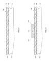
- FIGS. 2-13 are side cross-section views of the fabrication of an asymmetrical re-channel gallium nitride transistor, according to an embodiment of the present description.
- FIG. 14 is a flow chart of a process of fabricating an asymmetrical n-channel gallium nitride transistor, according to an embodiment of the present description.
- FIGS. 15 and 16 are schematics of a wireless power/charging device, according to an embodiment of the present description.
- over”, “to”, “between” and “on” as used herein may refer to a relative position of one layer with respect to other layers.
- One layer “over” or “on” another layer or bonded “to” another layer may be directly in contact with the other layer or may have one or more intervening layers.
- One layer “between” layers may be directly in contact with the layers or may have one or more intervening layers.
- Embodiments of the present description relate to n-channel gallium nitride transistors which include a recessed gate electrode wherein the polarization layer between the gate electrode and the gallium nitride layer is less than about 1 nm.
- the n-channel gallium nitride transistors may have an asymmetric configuration, wherein a gate-to drain length is greater than a gate-to-source length.
- the n-channel gallium nitride transistors may be utilized in wireless power/charging devices for improved efficiencies, longer transmission distances, and smaller form factors when compared with wireless power/charging devices using silicon-based transistors.
- FIG. 1 illustrates an n-channel gallium nitride transistor 100 according to embodiments of the present description.
- the n-channel gallium nitride transistor 100 may comprise a gallium nitride layer 102 having a source structure 104 and an opposing drain structure 106 formed therein.
- a charge inducing layer 108 may be formed on the gallium nitride layer 102 extending between the source structure 104 and the drain structure 106 (transistor width W), which forms a 2D electron gas (illustrated with dashed line 112 ) within the gallium nitride layer 102 .
- the charge inducing layer 108 may comprise a polarization layer 114 formed on a crystal transition layer 116 , wherein the crystal transition layer 116 abuts the gallium nitride layer 102 .
- the polarization layer 114 may have ternary crystal structure which forms the 2D electron gas 112 , but may inhibit electron mobility within the binary crystal structure of the gallium nitride layer 102 . Therefore, the crystal transition layer 116 may be a binary crystal structure which acts as a transition between the polarization layer 114 and the gallium nitride layer 102 . It is understood that although the charge inducing layer 108 is illustrated as having two layers (i.e. the polarization layer 114 and the crystal transition layer 116 ), it may be fabricated as a single layer (i.e. the polarization layer 114 only) or have more than two layers.
- the n-channel gallium nitride transistor 100 is an enhancement mode transistor.
- a portion of the polarization layer 114 may be removed proximate forming a recess 120 in a desired location for a gate electrode 122 to disrupt the 2D electron gas 112 , such that it does not extend through a gate length L g of the n-channel gallium nitride transistor 100 to achieve enhancement mode operation.
- a gate dielectric layer 118 may be formed over the polarization layer 114 and the gate electrode 122 may be formed on the gate dielectric layer 118 , such that the gate dielectric layer 118 electrically isolates the gate electrode 122 from the polarization layer 114 .
- source contacts 124 and drain contacts 126 may formed on the source structure 104 and the drain structure 106 , respectively, and may be utilized to form electrical connections with external components (not shown) through the formation of interconnection structure (not shown), as will be understood to those skilled in the art.
- the n-channel gallium nitride transistor 100 may include a gate-to-drain length L GD (i.e. from the gate to the drain structure 106 ) and a gate-to-source length L GS (i.e. from the gate to the source structure 104 ).
- the gate-to-drain length L GD may range from about 120 nm to about 400 nm.
- the gate-to-source length L GS may range from about 5 nm to about 400 nm.
- the gate length L G may range from about 20 nm to about 500 nm.
- the n-channel gallium nitride transistor 100 may have an asymmetric structure with a gate-to-drain length L GD (i.e. from the gate to the drain structure 106 ) larger than a gate-to-source length L GS (i.e. from the gate to the source structure 104 ), which will minimize resistance between across the gate-to-source length L GS , as will be understood to those skilled in the art.
- the polarization layer 114 may include, but is not limited to aluminum gallium nitride, aluminum indium nitride, and indium gallium nitride. In one embodiment, the polarization layer 114 is Al 0.83 In 0.17 N. In one embodiment, the polarization layer 114 may be have a thickness T 1 of between about 5 nm and 10 nm over the gate-to-drain length L GD area and over the gate-to-source length L GS area, which may achieve low on-state resistance. In a further embodiment, the polarization layer 114 may have a thickness T 2 of less than about 1 nm over the gate length L G area, which may achieve enhancement mode operation. In another embodiment, the crystal transition layer 116 may include, but is not limited to, indium nitride and aluminum nitride, and may have a thickness T 3 of less than about 1 nm.
- the gate dielectric layer 118 may be formed from any well-known gate dielectric material, including but not limited to silicon dioxide (SiO 2 ), silicon oxynitride (SiO x N y ), silicon nitride (Si 3 N 4 ), and high-k dielectric materials such as hafnium oxide, hafnium silicon oxide, lanthanum oxide, lanthanum aluminum oxide, zirconium oxide, zirconium silicon oxide, tantalum oxide, tantalum silicon oxide, titanium oxide, barium strontium titanium oxide, barium titanium oxide, strontium titanium oxide, yttrium oxide, aluminum oxide, lead scandium tantalum oxide, and lead zinc niobate.
- silicon dioxide SiO 2
- silicon oxynitride SiO x N y
- silicon nitride Si 3 N 4
- high-k dielectric materials such as hafnium oxide, hafnium silicon oxide, lanthanum oxide, lanthanum aluminum oxide, zirconium oxide, zir
- a high-K gate dielectric layer 118 may be advantageous to achieve low gate leakages.
- the gate dielectric layer 118 can be formed by well-known techniques, such as chemical vapor deposition (“CVD”), physical vapor deposition (“PVD”), atomic layer deposition (“ALD”).
- the gate electrode 122 can be formed of any suitable gate electrode material.
- the gate electrode 122 may be formed from materials that include, but are not limited to, polysilicon, tungsten, ruthenium, palladium, platinum, cobalt, nickel, hafnium, zirconium, titanium, tantalum, aluminum, titanium carbide, zirconium carbide, tantalum carbide, hafnium carbide, aluminum carbide, other metal carbides, metal nitrides, and metal oxides.
- the gate electrode 122 can be formed by well-known techniques, such as by blanket depositing a gate electrode material and then patterning the gate electrode material with well-known photolithography and etching techniques, as will be understood to those skilled in the art.
- Gallium nitride has a relatively wide bandgap (e.g. about 3.4 eV), when compared to the bandgap of silicon (about 1.1 eV). Therefore, the n-channel gallium nitride transistor 100 may withstand large electric fields, such as applied voltages, drain voltage, and the like, before suffering breakdown, when compared to a silicon based transistor of similar dimensions. This also enables n-channel gallium nitride transistors 100 to be scaled to even smaller physical dimensions while operating at the same supply voltage; thus, enabling small on-state resistance and smaller capacitance, which may result in reduced power dissipation and hence higher circuit efficiencies.
- the n-channel gallium nitride transistor 100 employs the 2D electron gas 112 as its electron transport channel for the operation thereof.
- the 2D electron gas 112 is formed at the abrupt hetero-interface formed by the deposition of the charge inducing layer 108 on the gallium nitride layer 102 through spontaneous and piezoelectric polarization, as will be understood to those skilled in the art.
- Very high charge densities up to about 2E13 per cm 2 can be formed by such a mechanism, without the use of impurity dopants, which allows for high electron mobility, e.g. greater than about 1000 cm 2 /V s (low sheet resistance at L GD and L GS regions).
- the n-channel gallium nitride transistor 100 may enable low parasitic leakages due to absence of band-to-band tunneling, low gate induced drain leakage (GIDL), and low generation of electron-hole pairs from impact ionization from hot electrons.
- GIDL gate induced drain leakage
- FIGS. 2-13 illustrate a process for forming a mirror image pair of n-channel gallium nitride transistors, according to one embodiment of the present description.
- a stacked substrate 130 may be formed comprising the charge inducing layer 108 formed on the gallium nitride layer 102 .
- the charge inducing layer 108 may comprise the polarization layer 114 formed on the crystal transition layer 116 , wherein the crystal transition layer 116 abuts the gallium nitride layer 102 .
- a hardmask 132 such as silicon nitride, silicon oxide, and the like, may be patterned by any known technique, such as photolithography, on the polarization layer 114 .
- the hardmask 132 may define a region for a shared drain for the mirror image pair of n-channel gallium nitride transistors to be formed.
- a first spacer material 142 may be deposited over the hardmask 132 and the gallium nitride layer 102 , as shown in FIG. 5 , the first spacer material 142 (see FIG. 4 ) may be etched to expose a top surface 134 of the hardmask 132 and expose portions of the polarization layer 114 , whereby first spacers 144 are formed on opposing sides 136 of the hardmask 132 .
- a width W 1 of the first spacers 144 may define the gate-to-drain length L GD (see FIG. 1 ) for each one of the pair of n-channel gallium nitride transistors to be formed.
- a second spacer material 152 may be deposited over the hardmask top surface 134 , the first spacers 144 , and the polarization layer 114 .
- the second spacer material 152 (see FIG. 6 ) may be etched to expose the hardmask top surface 134 , a top surface 146 of the first spacers 144 , and expose portions of the polarization layer 114 , whereby second spacers 154 are formed on opposing hardmask sides 136 abutting the first spacers 144 .
- a width W 2 of the second spacers 154 may define the channel or gate length L G (see FIG. 1 ) for each one of the pair of n-channel gallium nitride transistors.
- a third spacer material 162 may be deposited over the hardmask top surface 134 , the first spacers 144 , the second spacers 154 , and the polarization layer 114 .
- the third spacer material 162 (see FIG. 8 ) may be etched to expose the hardmask top surface 134 , the first spacer top surfaces 146 , a top surface 156 of the second spacers 154 , and portions of the polarization layer 114 , whereby third spacers 164 are formed on opposing hardmask sides 136 abutting the second spacers 154 .
- a width W 3 of the third spacers 164 may define the gate-to-source length L GS (see FIG. 1 ) for each one of the pair of n-channel gallium nitride transistors to be formed.
- the hardmask 132 may be removed and, using the first spacers 144 , the second spacers 154 , and the third spacers 164 as etch masks, recesses 172 may be formed to extend through the charge inducing layer 108 (e.g. the polarization layer 114 and the crystal transition layer 116 ) and into the gallium nitride layer 102 , by any known technique, such as etching.
- the recesses 172 may be formed with a plasma etch in a chlorine based chemistry.
- the source structures 104 and the shared drain structure 106 may be formed by epitaxial regrowth from the gallium nitride layer 102 .
- the regrowth process may comprise epitaxial crystal growth techniques, such as metal organic chemical vapor deposition (MOCVD) or molecular beam epitaxy (MBE).
- MOCVD metal organic chemical vapor deposition
- MBE molecular beam epitaxy
- the second spacers 154 may be removed, as well as a portion of the polarization layer 114 to form gate recesses 174 in the polarization layer 114 , which, as previously discussed, disrupts the 2D electron gas 112 , such that it does not extend through a gate length L g (previously labeled width W 2 ) to achieve enhancement mode operation.
- the gate dielectric layer 118 may be formed on the polarization layer 114 within the recesses 174 (see FIG. 12 ) and the gate electrodes 122 may be formed on the gate dielectric layer 118 such that the gate dielectric layer 118 electrically isolates the gate electrode 122 from the polarization layer 114 to from the n-channel gallium nitride transistors 100 1 and 100 2 .
- source contacts 124 and drain contacts 126 may be formed on the source structures 104 and the drain structure 106 , respectively.
- an interconnection structure (not shown) would be formed over the n-channel gallium nitride transistors 100 1 and 100 2 to appropriately connect the gate electrodes 122 , the source contacts 124 , and the drain contacts 126 with external components (not shown). However, for the sake of brevity and conciseness, the interconnection structure is not shown.
- FIG. 14 is a flow chart of a process 200 of fabricating an n-channel gallium nitride transistor according to an embodiment of the present description.
- a gallium nitride layer may be formed.
- a charge inducing layer may be formed on the gallium nitride layer to form a 2D electron gas within the gallium nitride layer, as set forth in block 204 .
- a source structure and a drain structure may be formed in the gallium nitride layer.
- a recess may be formed within the polarization layer between the source structure and the drain structure, wherein a thickness of a portion of the polarization layer which is between the recess and the gallium nitride layer is less than about 1 nm, as set in block 208 .
- a gate dielectric may be formed in the recess.
- a gate electrode may be formed adjacent the gate dielectric, as set forth in block 212 .
- FIG. 15 illustrates a wireless power/charging device 300 , according to an embodiment of the present description.
- the wireless power/charging device 300 may include a transmission module 310 and a receiving module 330 .
- the transmission module 310 may comprise a power unit 312 (such as an AC to DC converter), a transmitter 314 , a coil assembly 316 , a controller 318 , and a communication unit 322 (such as for radio frequency communication illustrated by arrows 324 ).
- the receiving module 330 such as components within a mobile device or a device which plugs into a mobile device, may comprise a load unit 332 which includes a voltage regulator and a battery, a rectifier 334 , a coil assembly 336 , a controller 338 , and a communication unit 342 (such as for radio frequency communication illustrated by arrows 344 ).
- a load unit 332 which includes a voltage regulator and a battery
- a rectifier 334 a rectifier 334
- a coil assembly 336 such as for radio frequency communication illustrated by arrows 344
- the specific interconnections and component operations of such a wireless power/charge device 300 are well known in the art and for the sake of brevity and conciseness will not be discussed herein.
- high voltage n-channel gallium nitride transistors 100 may be utilized in place of silicon power MOSFETs, as n-channel gallium nitride transistors have on-state resistances that are about three times better at the given breakdown voltage of 40V
- the n-channel gallium transistor 100 may be utilized in the transmitter 314 of the transmission module 310 .
- the transmitter 314 i.e. full-bridge inverter
- the transmitter 314 may have four n-channel gallium nitride transistors T 1 , T 2 , T 3 , and T 4 .
- the n-channel gallium nitride transistors T 1 , T 2 , T 3 , and T 4 may enable at least a 10% higher DC-to-AC conversion efficiency than silicon transistors.
- the use of the n-channel gallium nitride transistors T 1 , T 2 , T 3 , and T 4 may enable wireless power transmission over the air at 10 MHz or higher, which is over 100 times higher frequency than with comparable silicon transistors, and enabling distance transmission up to 2 meters (illustrated with an arrow 350 ), which is over 25 times longer than with comparable silicon transistors.
- the form factor of the transmission module coil assembly 316 and the receiving module coil assembly 336 may be as much as ten times thinner.
- utilizing the n-channel gallium nitride transistors 100 (see FIG. 1 ) in the voltage regulator of the receiving module load unit 332 may result in as much as a 100 times smaller form factor for the receiving module 330 and up to 7% higher efficiency than voltage regulators having silicon transistors. It is anticipated that an overall wireless power transmit efficiency improvement of 14% through the utilization n-channel gallium nitride transistors 100 (see FIG. 1 ) of the present description in the transmission module 310 and the receiving module 330 .
- the circuit design of a voltage regulator is well known in the art, and thus, for the sake of brevity and conciseness, is not illustrated with specificity.
- Example 1 is an re-channel gallium nitride transistor, comprising a gallium nitride layer; a source structure and a drain structure formed in the gallium nitride layer; a charge inducing layer comprising a polarization layer extending between the structure and the drain structure; a 2D electron gas within the gallium nitride layer; and a gate electrode extending at least partially into the polarization layer, wherein a thickness of a portion of the polarization layer which is between the gate electrode and the gallium nitride layer is less than about 1 nm.
- Example 2 the subject matter of Example 1 can optionally include a gate dielectric disposed between the gate electrode and the polarization layer.
- Example 3 the subject matter of either of Examples 1 or 2 can optionally include a portion of the polarization layer which is not between the gate electrode and the gallium nitride layer being between about 5 nm and 10 nm.
- Example 4 the subject matter of any of Examples 1 to 3 can optionally include the polarization layer being selected from the group consisting of aluminum gallium nitride, aluminum indium nitride, and indium gallium nitride.
- Example 5 the subject matter of any of Examples 1 to 4 can optionally include a crystal transition layer disposed between the gallium nitride layer and the polarization layer.
- Example 6 the subject matter of Example 5 can optionally include the crystal transition layer being selected from the group consisting of indium nitride and aluminum nitride.
- Example 7 the subject matter of any of Examples 1 to 6 can optionally include a gate-to-drain length between about 120 nm to about 400 nm and a gate-to-source length between about 5 nm to about 400 nm.
- Example 8 the subject matter of Example 7 can optionally include the gate-to drain length being greater than the gate-to-source length.
- Example 9 is a method of forming an n-channel gallium nitride transistor, comprising forming a gallium nitride layer; forming a charge inducing layer comprising a polarization layer on the gallium nitride layer to form a 2D electron gas within the gallium nitride layer; forming a source structure and a drain structure formed in the gallium nitride layer; forming a recess within the polarization layer between the source structure and the drain structure, wherein a thickness of a portion of the polarization layer which is between the recess and the gallium nitride layer is less than about 1 nm; forming asymmetrical dielectric spacers of different widths; forming a gate dielectric within the recess; and forming a gate electrode adjacent the gate dielectric.
- Example 10 the subject matter of Example 9 can optionally include forming the charge inducing layer comprising the polarization layer on the gallium nitride layer comprises forming the charge inducing layer comprising the polarization layer having a thickness of between about 5 nm and 10 nm.
- Example 11 the subject matter of either of Examples 9 or 10 can optionally include forming the polarization layer selected from the group consisting of aluminum gallium nitride, aluminum indium nitride, and indium gallium nitride.
- Example 12 the subject matter of any of Examples 9 to 11 can optionally include forming a crystal transition layer between the gallium nitride layer and the polarization layer.
- Example 13 the subject matter of Example 12 can optionally include forming the crystal transition layer from a material selected from the group consisting of indium nitride and aluminum nitride.
- Example 14 the subject matter of any of Examples 9 to 13 can optionally include forming a gate-to-drain length between about 120 nm to about 400 nm and forming a gate-to-source length between about 5 nm to about 400 nm.
- Example 15 the subject matter of Example 14 can optionally include the gate-to-drain length being greater than the gate-to-source length.
- Example 16 is a wireless power/charging device transmission module, comprising a coil assembly; and a transmitter, wherein the transmitter includes at least one n-channel gallium nitride transistor, comprising: a gallium nitride layer; a source structure and a drain structure formed in the gallium nitride layer; a charge inducing layer comprising a polarization layer extending between the structure and the drain structure; a 2D electron gas within the gallium nitride layer; and a gate electrode extending at least partially into the polarization layer.
- the transmitter includes at least one n-channel gallium nitride transistor, comprising: a gallium nitride layer; a source structure and a drain structure formed in the gallium nitride layer; a charge inducing layer comprising a polarization layer extending between the structure and the drain structure; a 2D electron gas within the gallium nitride layer; and a gate electrode extending at least partially into the polarization
- Example 17 the subject matter of Example 16 can optionally include a thickness of a portion of the polarization layer which is between the gate electrode and the gallium nitride layer being less than about 1 nm.
- Example 18 the subject matter of either of Example 16 or 17 can optionally include a gate dielectric disposed between the gate electrode and the polarization layer.
- Example 19 the subject matter of any of Examples 16 to 18 can optionally include a portion of the polarization layer which is between the gate electrode and the gallium nitride layer being between about 5 nm and 10 nm.
- Example 20 the subject matter of any of Example 16 to 19 can optionally include a crystal transition layer disposed between the gallium nitride layer and the polarization layer.
- Example 21 is a wireless power/charging device receiving module, comprising a coil assembly; a rectifier; and a load unit including a voltage regulator and a battery, wherein the voltage regulator includes at least one n-channel gallium nitride transistor, comprising: a gallium nitride layer; a source structure and a drain structure formed in the gallium nitride layer; a charge inducing layer comprising a polarization layer extending between the structure and the drain structure; a 2D electron gas within the gallium nitride layer; and a gate electrode extending at least partially into the polarization layer.
- the voltage regulator includes at least one n-channel gallium nitride transistor, comprising: a gallium nitride layer; a source structure and a drain structure formed in the gallium nitride layer; a charge inducing layer comprising a polarization layer extending between the structure and the drain structure; a 2D electron gas within the gallium nitride
- Example 22 the subject matter of Example 21 can optionally include a thickness of a portion of the polarization layer which is between the gate electrode and the gallium nitride layer being less than about 1 nm.
- Example 23 the subject matter of either of Example 21 or 22 can optionally include a gate dielectric disposed between the gate electrode and the polarization layer.
- Example 24 the subject matter of any of Examples 21 to 23 can optionally include a portion of the polarization layer which is between the gate electrode and the gallium nitride layer being between about 5 nm and 10 nm.
- Example 25 the subject matter of any of Example 21 to 24 can optionally include a crystal transition layer disposed between the gallium nitride layer and the polarization layer.
Landscapes
- Junction Field-Effect Transistors (AREA)
- Insulated Gate Type Field-Effect Transistor (AREA)
Applications Claiming Priority (1)
| Application Number | Priority Date | Filing Date | Title |
|---|---|---|---|
| PCT/US2014/071163 WO2016099509A1 (fr) | 2014-12-18 | 2014-12-18 | Transistors au nitrure de gallium de canal de type n |
Related Parent Applications (1)
| Application Number | Title | Priority Date | Filing Date |
|---|---|---|---|
| PCT/US2014/071163 A-371-Of-International WO2016099509A1 (fr) | 2014-12-18 | 2014-12-18 | Transistors au nitrure de gallium de canal de type n |
Related Child Applications (1)
| Application Number | Title | Priority Date | Filing Date |
|---|---|---|---|
| US16/041,657 Continuation US10756183B2 (en) | 2014-12-18 | 2018-07-20 | N-channel gallium nitride transistors |
Publications (2)
| Publication Number | Publication Date |
|---|---|
| US20180026097A1 US20180026097A1 (en) | 2018-01-25 |
| US10056456B2 true US10056456B2 (en) | 2018-08-21 |
Family
ID=56127158
Family Applications (2)
| Application Number | Title | Priority Date | Filing Date |
|---|---|---|---|
| US15/526,735 Active US10056456B2 (en) | 2014-12-18 | 2014-12-18 | N-channel gallium nitride transistors |
| US16/041,657 Active US10756183B2 (en) | 2014-12-18 | 2018-07-20 | N-channel gallium nitride transistors |
Family Applications After (1)
| Application Number | Title | Priority Date | Filing Date |
|---|---|---|---|
| US16/041,657 Active US10756183B2 (en) | 2014-12-18 | 2018-07-20 | N-channel gallium nitride transistors |
Country Status (6)
| Country | Link |
|---|---|
| US (2) | US10056456B2 (fr) |
| EP (1) | EP3235005A4 (fr) |
| KR (2) | KR102309482B1 (fr) |
| CN (1) | CN106922200B (fr) |
| TW (1) | TWI680582B (fr) |
| WO (1) | WO2016099509A1 (fr) |
Cited By (6)
| Publication number | Priority date | Publication date | Assignee | Title |
|---|---|---|---|---|
| US20180350911A1 (en) * | 2014-12-18 | 2018-12-06 | Intel Corporation | N-channel gallium nitride transistors |
| US10930500B2 (en) | 2014-09-18 | 2021-02-23 | Intel Corporation | Wurtzite heteroepitaxial structures with inclined sidewall facets for defect propagation control in silicon CMOS-compatible semiconductor devices |
| US11177376B2 (en) | 2014-09-25 | 2021-11-16 | Intel Corporation | III-N epitaxial device structures on free standing silicon mesas |
| US11233053B2 (en) | 2017-09-29 | 2022-01-25 | Intel Corporation | Group III-nitride (III-N) devices with reduced contact resistance and their methods of fabrication |
| US12125888B2 (en) | 2017-09-29 | 2024-10-22 | Intel Corporation | Group III-nitride (III-N) devices with reduced contact resistance and their methods of fabrication |
| US12249651B2 (en) | 2021-09-09 | 2025-03-11 | Samsung Electronics Co., Ltd. | Semiconductor device |
Families Citing this family (3)
| Publication number | Priority date | Publication date | Assignee | Title |
|---|---|---|---|---|
| WO2018063224A1 (fr) * | 2016-09-29 | 2018-04-05 | Intel Corporation | Contacts de jonction à effet tunnel inn pour canal p de gan |
| KR102887318B1 (ko) | 2020-12-30 | 2025-11-18 | 삼성전자주식회사 | 비대칭 활성 영역을 포함하는 이미지 센서 및 반도체 소자 |
| KR20240050587A (ko) * | 2022-10-12 | 2024-04-19 | 주식회사 디비하이텍 | 질화물계 반도체 소자 및 그 제조방법 |
Citations (6)
| Publication number | Priority date | Publication date | Assignee | Title |
|---|---|---|---|---|
| US20070045670A1 (en) * | 2005-08-31 | 2007-03-01 | Kabushiki Kaisha Toshiba | Nitride-based semiconductor device and method of manufacturing the same |
| US20100219452A1 (en) | 2009-02-27 | 2010-09-02 | Brierley Steven K | GaN HIGH ELECTRON MOBILITY TRANSISTOR (HEMT) STRUCTURES |
| US20100270559A1 (en) | 2007-11-19 | 2010-10-28 | Nec Corporation | Field effect transistor and process for manufacturing same |
| US20110278945A1 (en) | 2010-05-13 | 2011-11-17 | Qualcomm Incorporated | Resonance detection and control within a wireless power system |
| KR20120048244A (ko) | 2010-11-05 | 2012-05-15 | 삼성전자주식회사 | E-모드를 갖는 고 전자 이동도 트랜지스터 및 그 제조방법 |
| KR20130046249A (ko) | 2011-10-27 | 2013-05-07 | 삼성전자주식회사 | 전극구조체, 이를 포함하는 질화갈륨계 반도체소자 및 이들의 제조방법 |
Family Cites Families (125)
| Publication number | Priority date | Publication date | Assignee | Title |
|---|---|---|---|---|
| JPS5538658A (en) | 1978-09-09 | 1980-03-18 | Sony Corp | Recording and reproducing device |
| JPS5851575A (ja) | 1981-09-22 | 1983-03-26 | Fujitsu Ltd | 半導体装置の製造方法 |
| EP0283278B1 (fr) | 1987-03-18 | 1993-06-23 | Fujitsu Limited | Composé semi-conducteur à contacts ohmiques sans alliage |
| FR2689683B1 (fr) | 1992-04-07 | 1994-05-20 | Thomson Composants Microondes | Dispositif semiconducteur a transistors complementaires. |
| US5818078A (en) | 1994-08-29 | 1998-10-06 | Fujitsu Limited | Semiconductor device having a regrowth crystal region |
| JP2907128B2 (ja) | 1996-07-01 | 1999-06-21 | 日本電気株式会社 | 電界効果型トランジスタ及びその製造方法 |
| JP3813740B2 (ja) | 1997-07-11 | 2006-08-23 | Tdk株式会社 | 電子デバイス用基板 |
| FR2769924B1 (fr) | 1997-10-20 | 2000-03-10 | Centre Nat Rech Scient | Procede de realisation d'une couche epitaxiale de nitrure de gallium, couche epitaxiale de nitrure de gallium et composant optoelectronique muni d'une telle couche |
| US6608327B1 (en) | 1998-02-27 | 2003-08-19 | North Carolina State University | Gallium nitride semiconductor structure including laterally offset patterned layers |
| JP4540146B2 (ja) | 1998-12-24 | 2010-09-08 | ルネサスエレクトロニクス株式会社 | 半導体装置の製造方法 |
| JP3555500B2 (ja) | 1999-05-21 | 2004-08-18 | 豊田合成株式会社 | Iii族窒化物半導体及びその製造方法 |
| US6521514B1 (en) | 1999-11-17 | 2003-02-18 | North Carolina State University | Pendeoepitaxial methods of fabricating gallium nitride semiconductor layers on sapphire substrates |
| JP4667556B2 (ja) | 2000-02-18 | 2011-04-13 | 古河電気工業株式会社 | 縦型GaN系電界効果トランジスタ、バイポーラトランジスタと縦型GaN系電界効果トランジスタの製造方法 |
| US6261929B1 (en) | 2000-02-24 | 2001-07-17 | North Carolina State University | Methods of forming a plurality of semiconductor layers using spaced trench arrays |
| JP2002249400A (ja) | 2001-02-22 | 2002-09-06 | Mitsubishi Chemicals Corp | 化合物半導体単結晶の製造方法およびその利用 |
| US20040029365A1 (en) | 2001-05-07 | 2004-02-12 | Linthicum Kevin J. | Methods of fabricating gallium nitride microelectronic layers on silicon layers and gallium nitride microelectronic structures formed thereby |
| WO2002099859A1 (fr) | 2001-06-04 | 2002-12-12 | Toyoda Gosei Co., Ltd. | Procede de production d'un semiconducteur au nitrure iii |
| JP2003069010A (ja) | 2001-08-24 | 2003-03-07 | Sharp Corp | 半導体装置およびその製造方法 |
| JP2003077847A (ja) | 2001-09-06 | 2003-03-14 | Sumitomo Chem Co Ltd | 3−5族化合物半導体の製造方法 |
| US7501669B2 (en) | 2003-09-09 | 2009-03-10 | Cree, Inc. | Wide bandgap transistor devices with field plates |
| JP5194334B2 (ja) | 2004-05-18 | 2013-05-08 | 住友電気工業株式会社 | Iii族窒化物半導体デバイスの製造方法 |
| JP4571476B2 (ja) | 2004-10-18 | 2010-10-27 | ローム株式会社 | 半導体装置の製造方法 |
| US7834380B2 (en) | 2004-12-09 | 2010-11-16 | Panasonic Corporation | Field effect transistor and method for fabricating the same |
| JP4697397B2 (ja) | 2005-02-16 | 2011-06-08 | サンケン電気株式会社 | 複合半導体装置 |
| US20060197129A1 (en) | 2005-03-03 | 2006-09-07 | Triquint Semiconductor, Inc. | Buried and bulk channel finFET and method of making the same |
| US8324660B2 (en) | 2005-05-17 | 2012-12-04 | Taiwan Semiconductor Manufacturing Company, Ltd. | Lattice-mismatched semiconductor structures with reduced dislocation defect densities and related methods for device fabrication |
| US9153645B2 (en) | 2005-05-17 | 2015-10-06 | Taiwan Semiconductor Manufacturing Company, Ltd. | Lattice-mismatched semiconductor structures with reduced dislocation defect densities and related methods for device fabrication |
| JP2007165431A (ja) | 2005-12-12 | 2007-06-28 | Nippon Telegr & Teleph Corp <Ntt> | 電界効果型トランジスタおよびその製造方法 |
| KR101019941B1 (ko) | 2006-03-10 | 2011-03-09 | 에스티씨. 유엔엠 | Gan 나노선의 펄스 성장 및 ⅲ 족 질화물 반도체 기판 물질과 디바이스에서의 어플리케이션 |
| US7777250B2 (en) | 2006-03-24 | 2010-08-17 | Taiwan Semiconductor Manufacturing Company, Ltd. | Lattice-mismatched semiconductor structures and related methods for device fabrication |
| JP5179023B2 (ja) | 2006-05-31 | 2013-04-10 | パナソニック株式会社 | 電界効果トランジスタ |
| JP2008004720A (ja) | 2006-06-22 | 2008-01-10 | Nippon Telegr & Teleph Corp <Ntt> | 窒化物半導体を用いたヘテロ構造電界効果トランジスタ |
| US7803690B2 (en) | 2006-06-23 | 2010-09-28 | Taiwan Semiconductor Manufacturing Company, Ltd. | Epitaxy silicon on insulator (ESOI) |
| US8188573B2 (en) | 2006-08-31 | 2012-05-29 | Industrial Technology Research Institute | Nitride semiconductor structure |
| US8173551B2 (en) | 2006-09-07 | 2012-05-08 | Taiwan Semiconductor Manufacturing Co., Ltd. | Defect reduction using aspect ratio trapping |
| WO2008036256A1 (fr) | 2006-09-18 | 2008-03-27 | Amberwave Systems Corporation | Piégeage de rapport hauteur/largeur pour applications à signaux mixtes |
| WO2008051503A2 (fr) | 2006-10-19 | 2008-05-02 | Amberwave Systems Corporation | Dispositifs base sur une source de lumière munie de structures semi-conductrices a désaccord de réseau |
| US7692198B2 (en) | 2007-02-19 | 2010-04-06 | Alcatel-Lucent Usa Inc. | Wide-bandgap semiconductor devices |
| JP2008305816A (ja) | 2007-06-05 | 2008-12-18 | Mitsubishi Electric Corp | 半導体装置及びその製造方法 |
| US20090278233A1 (en) | 2007-07-26 | 2009-11-12 | Pinnington Thomas Henry | Bonded intermediate substrate and method of making same |
| JP5348364B2 (ja) | 2007-08-27 | 2013-11-20 | サンケン電気株式会社 | ヘテロ接合型電界効果半導体装置 |
| JP4784609B2 (ja) | 2008-01-21 | 2011-10-05 | Tdk株式会社 | 電子デバイス用基板 |
| US8519438B2 (en) * | 2008-04-23 | 2013-08-27 | Transphorm Inc. | Enhancement mode III-N HEMTs |
| US7952150B1 (en) | 2008-06-05 | 2011-05-31 | Rf Micro Devices, Inc. | Enhancement mode MOSFET and depletion mode FET on a common group III-V substrate |
| US8981427B2 (en) | 2008-07-15 | 2015-03-17 | Taiwan Semiconductor Manufacturing Company, Ltd. | Polishing of small composite semiconductor materials |
| US8309987B2 (en) | 2008-07-15 | 2012-11-13 | Imec | Enhancement mode semiconductor device |
| TWI425558B (zh) | 2008-08-11 | 2014-02-01 | 台灣積體電路製造股份有限公司 | 形成電路結構的方法 |
| US8367520B2 (en) | 2008-09-22 | 2013-02-05 | Soitec | Methods and structures for altering strain in III-nitride materials |
| US20100140735A1 (en) | 2008-12-10 | 2010-06-10 | Epir Technologies, Inc. | Nanostructures for dislocation blocking in group ii-vi semiconductor devices |
| JP5487615B2 (ja) * | 2008-12-24 | 2014-05-07 | サンケン電気株式会社 | 電界効果半導体装置及びその製造方法 |
| JP5737948B2 (ja) | 2008-12-26 | 2015-06-17 | ルネサスエレクトロニクス株式会社 | ヘテロ接合電界効果トランジスタ、ヘテロ接合電界トランジスタの製造方法、および電子装置 |
| US8313967B1 (en) | 2009-01-21 | 2012-11-20 | Stc.Unm | Cubic phase, nitrogen-based compound semiconductor films epitaxially grown on a grooved Si <001> substrate |
| JP5469098B2 (ja) | 2009-01-22 | 2014-04-09 | パナソニック株式会社 | 電界効果トランジスタ及びその製造方法 |
| US8497658B2 (en) * | 2009-01-22 | 2013-07-30 | Qualcomm Incorporated | Adaptive power control for wireless charging of devices |
| US8507304B2 (en) | 2009-07-17 | 2013-08-13 | Applied Materials, Inc. | Method of forming a group III-nitride crystalline film on a patterned substrate by hydride vapor phase epitaxy (HVPE) |
| JP5529595B2 (ja) | 2009-07-30 | 2014-06-25 | 住友電気工業株式会社 | 半導体装置及びその製造方法 |
| KR101640830B1 (ko) | 2009-08-17 | 2016-07-22 | 삼성전자주식회사 | 기판 구조체 및 그 제조 방법 |
| JP5609055B2 (ja) | 2009-10-02 | 2014-10-22 | 富士通株式会社 | 化合物半導体装置及びその製造方法 |
| CN102598215A (zh) | 2009-11-26 | 2012-07-18 | 住友化学株式会社 | 半导体基板及半导体基板的制造方法 |
| JP5590874B2 (ja) | 2009-12-18 | 2014-09-17 | パナソニック株式会社 | 窒化物半導体素子 |
| JP5505698B2 (ja) | 2010-02-01 | 2014-05-28 | 日本電信電話株式会社 | 半導体装置 |
| US20110210377A1 (en) | 2010-02-26 | 2011-09-01 | Infineon Technologies Austria Ag | Nitride semiconductor device |
| GB2482308A (en) | 2010-07-28 | 2012-02-01 | Univ Sheffield | Super junction silicon devices |
| US8389348B2 (en) | 2010-09-14 | 2013-03-05 | Taiwan Semiconductor Manufacturing Company, Ltd. | Mechanism of forming SiC crystalline on Si substrates to allow integration of GaN and Si electronics |
| US8709921B2 (en) | 2010-11-15 | 2014-04-29 | Applied Materials, Inc. | Method for forming a semiconductor device using selective epitaxy of group III-nitride |
| US8383471B1 (en) * | 2011-04-11 | 2013-02-26 | Hrl Laboratories, Llc | Self aligned sidewall gate GaN HEMT |
| TWI544628B (zh) | 2011-05-16 | 2016-08-01 | 瑞薩電子股份有限公司 | Field effect transistor and semiconductor device |
| US8835988B2 (en) | 2011-06-06 | 2014-09-16 | Eta Semiconductor Inc. | Hybrid monolithic integration |
| TW201306235A (zh) | 2011-06-10 | 2013-02-01 | 住友化學股份有限公司 | 半導體裝置、半導體基板、半導體基板之製造方法及半導體裝置之製造方法 |
| JP5942204B2 (ja) | 2011-07-01 | 2016-06-29 | パナソニックIpマネジメント株式会社 | 半導体装置 |
| US9087741B2 (en) | 2011-07-11 | 2015-07-21 | International Business Machines Corporation | CMOS with dual raised source and drain for NMOS and PMOS |
| US8507920B2 (en) | 2011-07-11 | 2013-08-13 | Taiwan Semiconductor Manufacturing Company, Ltd. | Semiconductor structure and method of forming the same |
| JP2013041986A (ja) | 2011-08-16 | 2013-02-28 | Advanced Power Device Research Association | GaN系半導体装置 |
| US9112048B2 (en) | 2011-08-17 | 2015-08-18 | Ramgoss Inc. | Vertical field effect transistor on oxide semiconductor substrate |
| JP5757195B2 (ja) | 2011-08-23 | 2015-07-29 | セイコーエプソン株式会社 | 半導体装置、電気光学装置、電力変換装置及び電子機器 |
| US20130105817A1 (en) * | 2011-10-26 | 2013-05-02 | Triquint Semiconductor, Inc. | High electron mobility transistor structure and method |
| US8841703B2 (en) | 2011-10-31 | 2014-09-23 | Taiwan Semiconductor Manufacturing Company, Ltd. | High electron mobility transistor and method of forming the same |
| JP5953706B2 (ja) | 2011-11-02 | 2016-07-20 | 富士通株式会社 | 化合物半導体装置及びその製造方法 |
| US8530978B1 (en) | 2011-12-06 | 2013-09-10 | Hrl Laboratories, Llc | High current high voltage GaN field effect transistors and method of fabricating same |
| US9240410B2 (en) | 2011-12-19 | 2016-01-19 | Intel Corporation | Group III-N nanowire transistors |
| KR101681396B1 (ko) | 2011-12-19 | 2016-11-30 | 인텔 코포레이션 | 고전압 트랜지스터와 그 제조방법, 고전압 트랜지스터를 포함하는 시스템 온 칩 및 고전압 트랜지스터를 포함하는 이동 컴퓨팅 장치 |
| CN107275287B (zh) | 2011-12-19 | 2021-08-13 | 英特尔公司 | 用于集成有功率管理和射频电路的片上系统(soc)结构的iii族-n晶体管 |
| KR20140097464A (ko) | 2011-12-20 | 2014-08-06 | 인텔 코오퍼레이션 | n-형 및 p-형 MOS 소스-드레인 콘택들을 위한 III-V 층들 |
| US9000464B2 (en) | 2012-03-01 | 2015-04-07 | Design Express Limited | Semiconductor structure for substrate separation and method for manufacturing the same |
| US8836016B2 (en) | 2012-03-08 | 2014-09-16 | Taiwan Semiconductor Manufacturing Company, Ltd. | Semiconductor structures and methods with high mobility and high energy bandgap materials |
| US9111905B2 (en) | 2012-03-29 | 2015-08-18 | Taiwan Semiconductor Manufacturing Company, Ltd. | High electron mobility transistor and method of forming the same |
| US9142649B2 (en) | 2012-04-23 | 2015-09-22 | United Microelectronics Corp. | Semiconductor structure with metal gate and method of fabricating the same |
| US20130313561A1 (en) | 2012-05-25 | 2013-11-28 | Triquint Semiconductor, Inc. | Group iii-nitride transistor with charge-inducing layer |
| JP5972065B2 (ja) | 2012-06-20 | 2016-08-17 | 富士フイルム株式会社 | 薄膜トランジスタの製造方法 |
| US8975664B2 (en) * | 2012-06-27 | 2015-03-10 | Triquint Semiconductor, Inc. | Group III-nitride transistor using a regrown structure |
| US8772786B2 (en) | 2012-07-13 | 2014-07-08 | Raytheon Company | Gallium nitride devices having low ohmic contact resistance |
| US8912570B2 (en) | 2012-08-09 | 2014-12-16 | Taiwan Semiconductor Manufacturing Company, Ltd. | High electron mobility transistor and method of forming the same |
| KR101927411B1 (ko) | 2012-09-28 | 2018-12-10 | 삼성전자주식회사 | 2deg와 2dhg를 이용한 반도체 소자 및 제조방법 |
| US9583574B2 (en) | 2012-09-28 | 2017-02-28 | Intel Corporation | Epitaxial buffer layers for group III-N transistors on silicon substrates |
| US9099490B2 (en) | 2012-09-28 | 2015-08-04 | Intel Corporation | Self-aligned structures and methods for asymmetric GaN transistors and enhancement mode operation |
| US9064709B2 (en) | 2012-09-28 | 2015-06-23 | Intel Corporation | High breakdown voltage III-N depletion mode MOS capacitors |
| JP2014078653A (ja) | 2012-10-12 | 2014-05-01 | Waseda Univ | Iii族窒化物半導体層の製造方法 |
| EP2743965B1 (fr) | 2012-12-13 | 2015-07-08 | Imec | Procédé de fabrication de dispositifs semi-conducteurs |
| US9196709B2 (en) | 2013-02-01 | 2015-11-24 | Taiwan Semiconductor Manufacturing Company, Ltd. | Methods for forming semiconductor regions in trenches |
| US9331244B2 (en) | 2013-02-25 | 2016-05-03 | Sensor Electronic Technology, Inc. | Semiconductor structure with inhomogeneous regions |
| KR102036349B1 (ko) | 2013-03-08 | 2019-10-24 | 삼성전자 주식회사 | 고 전자이동도 트랜지스터 |
| US9012261B2 (en) | 2013-03-13 | 2015-04-21 | Intermolecular, Inc. | High productivity combinatorial screening for stable metal oxide TFTs |
| US9129889B2 (en) | 2013-03-15 | 2015-09-08 | Semiconductor Components Industries, Llc | High electron mobility semiconductor device and method therefor |
| US9006791B2 (en) | 2013-03-15 | 2015-04-14 | The Government Of The United States Of America, As Represented By The Secretary Of The Navy | III-nitride P-channel field effect transistor with hole carriers in the channel |
| JP5954831B2 (ja) | 2013-03-26 | 2016-07-20 | トヨタ自動車株式会社 | 半導体装置の製造方法 |
| JP6197422B2 (ja) | 2013-07-11 | 2017-09-20 | 富士通セミコンダクター株式会社 | 半導体装置の製造方法および支持基板付きウェハ |
| JP6179266B2 (ja) | 2013-08-12 | 2017-08-16 | 富士通株式会社 | 半導体装置及び半導体装置の製造方法 |
| US20150041820A1 (en) | 2013-08-12 | 2015-02-12 | Philippe Renaud | Complementary gallium nitride integrated circuits and methods of their fabrication |
| GB2517697A (en) | 2013-08-27 | 2015-03-04 | Ibm | Compound semiconductor structure |
| TWI521664B (zh) | 2013-09-03 | 2016-02-11 | 瑞昱半導體股份有限公司 | 金屬溝渠去耦合電容結構與形成金屬溝渠去耦合電容結構的方法 |
| KR102130460B1 (ko) | 2013-09-27 | 2020-07-07 | 인텔 코포레이션 | Si 웨이퍼들 상의 ⅲ-ⅴ 디바이스들의 집적화 |
| US9324802B2 (en) | 2013-10-31 | 2016-04-26 | Infineon Technologies Austria | Spacer supported lateral channel FET |
| WO2015077647A2 (fr) | 2013-11-22 | 2015-05-28 | Cambridge Electronics, Inc. | Gestion de champ électrique pour un semi-conducteur au nitrure du groupe iii |
| JP6240778B2 (ja) | 2013-12-06 | 2017-11-29 | ポスコPosco | 極低温衝撃靭性に優れた高強度溶接継手部及びこのためのフラックスコアードアーク溶接用ワイヤ |
| US9640422B2 (en) | 2014-01-23 | 2017-05-02 | Intel Corporation | III-N devices in Si trenches |
| WO2015125471A1 (fr) | 2014-02-21 | 2015-08-27 | パナソニック株式会社 | Transistor à effet de champ |
| JP6302303B2 (ja) | 2014-03-17 | 2018-03-28 | 株式会社東芝 | 半導体発光素子 |
| US9666708B2 (en) | 2014-03-26 | 2017-05-30 | Intel Corporation | III-N transistors with enhanced breakdown voltage |
| US9331076B2 (en) | 2014-05-02 | 2016-05-03 | International Business Machines Corporation | Group III nitride integration with CMOS technology |
| US10325774B2 (en) | 2014-09-18 | 2019-06-18 | Intel Corporation | Wurtzite heteroepitaxial structures with inclined sidewall facets for defect propagation control in silicon CMOS-compatible semiconductor devices |
| US10229991B2 (en) | 2014-09-25 | 2019-03-12 | Intel Corporation | III-N epitaxial device structures on free standing silicon mesas |
| US9496379B2 (en) | 2014-10-20 | 2016-11-15 | International Business Machines Corporation | Method and structure for III-V FinFET |
| KR102238547B1 (ko) | 2014-10-30 | 2021-04-09 | 인텔 코포레이션 | 질화 갈륨 트랜지스터에서 2d 전자 가스에 대한 낮은 접촉 저항을 위한 소스/드레인 재성장 |
| EP3235005A4 (fr) * | 2014-12-18 | 2018-09-12 | Intel Corporation | Transistors au nitrure de gallium de canal de type n |
| CN107660313B (zh) | 2015-06-26 | 2022-09-13 | 英特尔公司 | 在衬底上的氮化镓(GaN)晶体管结构 |
-
2014
- 2014-12-18 EP EP14908596.1A patent/EP3235005A4/fr not_active Withdrawn
- 2014-12-18 CN CN201480083467.5A patent/CN106922200B/zh active Active
- 2014-12-18 US US15/526,735 patent/US10056456B2/en active Active
- 2014-12-18 WO PCT/US2014/071163 patent/WO2016099509A1/fr not_active Ceased
- 2014-12-18 KR KR1020177013159A patent/KR102309482B1/ko active Active
- 2014-12-18 KR KR1020217031358A patent/KR102423219B1/ko active Active
-
2015
- 2015-11-17 TW TW104137900A patent/TWI680582B/zh active
-
2018
- 2018-07-20 US US16/041,657 patent/US10756183B2/en active Active
Patent Citations (6)
| Publication number | Priority date | Publication date | Assignee | Title |
|---|---|---|---|---|
| US20070045670A1 (en) * | 2005-08-31 | 2007-03-01 | Kabushiki Kaisha Toshiba | Nitride-based semiconductor device and method of manufacturing the same |
| US20100270559A1 (en) | 2007-11-19 | 2010-10-28 | Nec Corporation | Field effect transistor and process for manufacturing same |
| US20100219452A1 (en) | 2009-02-27 | 2010-09-02 | Brierley Steven K | GaN HIGH ELECTRON MOBILITY TRANSISTOR (HEMT) STRUCTURES |
| US20110278945A1 (en) | 2010-05-13 | 2011-11-17 | Qualcomm Incorporated | Resonance detection and control within a wireless power system |
| KR20120048244A (ko) | 2010-11-05 | 2012-05-15 | 삼성전자주식회사 | E-모드를 갖는 고 전자 이동도 트랜지스터 및 그 제조방법 |
| KR20130046249A (ko) | 2011-10-27 | 2013-05-07 | 삼성전자주식회사 | 전극구조체, 이를 포함하는 질화갈륨계 반도체소자 및 이들의 제조방법 |
Non-Patent Citations (2)
| Title |
|---|
| International Preliminary Report on Patentability from PCT/US2014/071163 dated Jun. 29, 2017, 3 pgs. |
| International Search Report and Written Opinion from PCT/US2014/071163 dated Sep. 17, 2015, 13 pgs. |
Cited By (8)
| Publication number | Priority date | Publication date | Assignee | Title |
|---|---|---|---|---|
| US10930500B2 (en) | 2014-09-18 | 2021-02-23 | Intel Corporation | Wurtzite heteroepitaxial structures with inclined sidewall facets for defect propagation control in silicon CMOS-compatible semiconductor devices |
| US11177376B2 (en) | 2014-09-25 | 2021-11-16 | Intel Corporation | III-N epitaxial device structures on free standing silicon mesas |
| US20180350911A1 (en) * | 2014-12-18 | 2018-12-06 | Intel Corporation | N-channel gallium nitride transistors |
| US10756183B2 (en) * | 2014-12-18 | 2020-08-25 | Intel Corporation | N-channel gallium nitride transistors |
| US11233053B2 (en) | 2017-09-29 | 2022-01-25 | Intel Corporation | Group III-nitride (III-N) devices with reduced contact resistance and their methods of fabrication |
| US11728346B2 (en) | 2017-09-29 | 2023-08-15 | Intel Corporation | Group III-nitride (III-N) devices with reduced contact resistance and their methods of fabrication |
| US12125888B2 (en) | 2017-09-29 | 2024-10-22 | Intel Corporation | Group III-nitride (III-N) devices with reduced contact resistance and their methods of fabrication |
| US12249651B2 (en) | 2021-09-09 | 2025-03-11 | Samsung Electronics Co., Ltd. | Semiconductor device |
Also Published As
| Publication number | Publication date |
|---|---|
| KR102423219B1 (ko) | 2022-07-20 |
| WO2016099509A1 (fr) | 2016-06-23 |
| CN106922200B (zh) | 2021-11-09 |
| TWI680582B (zh) | 2019-12-21 |
| KR102309482B1 (ko) | 2021-10-07 |
| US10756183B2 (en) | 2020-08-25 |
| US20180350911A1 (en) | 2018-12-06 |
| CN106922200A (zh) | 2017-07-04 |
| KR20170097611A (ko) | 2017-08-28 |
| TW201633543A (zh) | 2016-09-16 |
| US20180026097A1 (en) | 2018-01-25 |
| EP3235005A1 (fr) | 2017-10-25 |
| EP3235005A4 (fr) | 2018-09-12 |
| KR20210122906A (ko) | 2021-10-12 |
Similar Documents
| Publication | Publication Date | Title |
|---|---|---|
| US10756183B2 (en) | N-channel gallium nitride transistors | |
| CN103930997B (zh) | 具有凹陷电极结构的半导体器件 | |
| US10573647B2 (en) | CMOS circuits using n-channel and p-channel gallium nitride transistors | |
| US9306051B2 (en) | Semiconductor device using a nitride semiconductor | |
| US20110186927A1 (en) | Power semiconductor device | |
| KR102238547B1 (ko) | 질화 갈륨 트랜지스터에서 2d 전자 가스에 대한 낮은 접촉 저항을 위한 소스/드레인 재성장 | |
| US9478651B2 (en) | Breakdown voltage multiplying integration scheme | |
| US20100084688A1 (en) | Enhancement-mode nitride transistor | |
| JP2015046444A (ja) | 半導体装置 | |
| EP3084834A1 (fr) | Couches de revêtement à double contrainte pour dispositifs à semi-conducteurs | |
| US8716782B2 (en) | Power semiconductor device having a thin gate insulating film with high-k dielectric materials and method for manufacturing the same | |
| Lu et al. | GaN power electronics | |
| US20250359264A1 (en) | Lateral diffusion metal oxide semiconductor (ldmos) transistor and method of making | |
| Lei | Multifunctional Gan-On-Si Power Devices Based on Double-Channel Heterostructure | |
| CN119562569A (zh) | 芯片及其制备方法、电子设备 |
Legal Events
| Date | Code | Title | Description |
|---|---|---|---|
| STCF | Information on status: patent grant |
Free format text: PATENTED CASE |
|
| MAFP | Maintenance fee payment |
Free format text: PAYMENT OF MAINTENANCE FEE, 4TH YEAR, LARGE ENTITY (ORIGINAL EVENT CODE: M1551); ENTITY STATUS OF PATENT OWNER: LARGE ENTITY Year of fee payment: 4 |
|
| FEPP | Fee payment procedure |
Free format text: MAINTENANCE FEE REMINDER MAILED (ORIGINAL EVENT CODE: REM.); ENTITY STATUS OF PATENT OWNER: LARGE ENTITY |