US11177655B2 - Multi-line supply unit for a vehicle control unit - Google Patents
Multi-line supply unit for a vehicle control unit Download PDFInfo
- Publication number
- US11177655B2 US11177655B2 US16/647,190 US201816647190A US11177655B2 US 11177655 B2 US11177655 B2 US 11177655B2 US 201816647190 A US201816647190 A US 201816647190A US 11177655 B2 US11177655 B2 US 11177655B2
- Authority
- US
- United States
- Prior art keywords
- supply
- line
- supply lines
- voltage
- control unit
- Prior art date
- Legal status (The legal status is an assumption and is not a legal conclusion. Google has not performed a legal analysis and makes no representation as to the accuracy of the status listed.)
- Active
Links
Images




Classifications
-
- H—ELECTRICITY
- H02—GENERATION; CONVERSION OR DISTRIBUTION OF ELECTRIC POWER
- H02H—EMERGENCY PROTECTIVE CIRCUIT ARRANGEMENTS
- H02H7/00—Emergency protective circuit arrangements specially adapted for specific types of electric machines or apparatus or for sectionalised protection of cable or line systems, and effecting automatic switching in the event of an undesired change from normal working conditions
- H02H7/20—Emergency protective circuit arrangements specially adapted for specific types of electric machines or apparatus or for sectionalised protection of cable or line systems, and effecting automatic switching in the event of an undesired change from normal working conditions for electronic equipment
-
- H—ELECTRICITY
- H02—GENERATION; CONVERSION OR DISTRIBUTION OF ELECTRIC POWER
- H02J—ELECTRIC POWER NETWORKS; CIRCUIT ARRANGEMENTS OR SYSTEMS FOR SUPPLYING OR DISTRIBUTING ELECTRIC POWER; SYSTEMS FOR STORING ELECTRIC ENERGY
- H02J1/00—Circuit arrangements for DC mains or DC distribution networks
- H02J1/10—Parallel operation of DC sources
- H02J1/108—Parallel operation of DC sources having arrangements for blocking reverse current flow, e.g. using diodes
-
- H—ELECTRICITY
- H02—GENERATION; CONVERSION OR DISTRIBUTION OF ELECTRIC POWER
- H02J—ELECTRIC POWER NETWORKS; CIRCUIT ARRANGEMENTS OR SYSTEMS FOR SUPPLYING OR DISTRIBUTING ELECTRIC POWER; SYSTEMS FOR STORING ELECTRIC ENERGY
- H02J3/00—Circuit arrangements for AC mains or AC distribution networks
- H02J3/38—Arrangements for feeding a single network from two or more generators or sources in parallel; Arrangements for feeding already energised networks from additional generators or sources in parallel
-
- G—PHYSICS
- G05—CONTROLLING; REGULATING
- G05B—CONTROL OR REGULATING SYSTEMS IN GENERAL; FUNCTIONAL ELEMENTS OF SUCH SYSTEMS; MONITORING OR TESTING ARRANGEMENTS FOR SUCH SYSTEMS OR ELEMENTS
- G05B19/00—Program-control systems
- G05B19/02—Program-control systems electric
- G05B19/04—Program control other than numerical control, i.e. in sequence controllers or logic controllers
- G05B19/042—Program control other than numerical control, i.e. in sequence controllers or logic controllers using digital processors
-
- H—ELECTRICITY
- H02—GENERATION; CONVERSION OR DISTRIBUTION OF ELECTRIC POWER
- H02H—EMERGENCY PROTECTIVE CIRCUIT ARRANGEMENTS
- H02H1/00—Details of emergency protective circuit arrangements
- H02H1/06—Arrangements for supplying operative power
-
- H—ELECTRICITY
- H02—GENERATION; CONVERSION OR DISTRIBUTION OF ELECTRIC POWER
- H02H—EMERGENCY PROTECTIVE CIRCUIT ARRANGEMENTS
- H02H11/00—Emergency protective circuit arrangements for preventing the switching-on in case an undesired electric working condition might result
- H02H11/002—Emergency protective circuit arrangements for preventing the switching-on in case an undesired electric working condition might result in case of inverted polarity or connection; with switching for obtaining correct connection
-
- H—ELECTRICITY
- H02—GENERATION; CONVERSION OR DISTRIBUTION OF ELECTRIC POWER
- H02H—EMERGENCY PROTECTIVE CIRCUIT ARRANGEMENTS
- H02H11/00—Emergency protective circuit arrangements for preventing the switching-on in case an undesired electric working condition might result
- H02H11/002—Emergency protective circuit arrangements for preventing the switching-on in case an undesired electric working condition might result in case of inverted polarity or connection; with switching for obtaining correct connection
- H02H11/003—Emergency protective circuit arrangements for preventing the switching-on in case an undesired electric working condition might result in case of inverted polarity or connection; with switching for obtaining correct connection using a field effect transistor as protecting element in one of the supply lines
-
- H—ELECTRICITY
- H02—GENERATION; CONVERSION OR DISTRIBUTION OF ELECTRIC POWER
- H02H—EMERGENCY PROTECTIVE CIRCUIT ARRANGEMENTS
- H02H3/00—Emergency protective circuit arrangements for automatic disconnection directly responsive to an undesired change from normal electric working condition with or without subsequent reconnection ; integrated protection
- H02H3/20—Emergency protective circuit arrangements for automatic disconnection directly responsive to an undesired change from normal electric working condition with or without subsequent reconnection ; integrated protection responsive to excess voltage
-
- H—ELECTRICITY
- H02—GENERATION; CONVERSION OR DISTRIBUTION OF ELECTRIC POWER
- H02H—EMERGENCY PROTECTIVE CIRCUIT ARRANGEMENTS
- H02H7/00—Emergency protective circuit arrangements specially adapted for specific types of electric machines or apparatus or for sectionalised protection of cable or line systems, and effecting automatic switching in the event of an undesired change from normal working conditions
- H02H7/26—Sectionalised protection of cable or line systems, e.g. for disconnecting a section on which a short-circuit, earth fault, or arc discharge has occured
-
- H—ELECTRICITY
- H02—GENERATION; CONVERSION OR DISTRIBUTION OF ELECTRIC POWER
- H02H—EMERGENCY PROTECTIVE CIRCUIT ARRANGEMENTS
- H02H7/00—Emergency protective circuit arrangements specially adapted for specific types of electric machines or apparatus or for sectionalised protection of cable or line systems, and effecting automatic switching in the event of an undesired change from normal working conditions
- H02H7/26—Sectionalised protection of cable or line systems, e.g. for disconnecting a section on which a short-circuit, earth fault, or arc discharge has occured
- H02H7/268—Sectionalised protection of cable or line systems, e.g. for disconnecting a section on which a short-circuit, earth fault, or arc discharge has occured for DC systems
-
- H—ELECTRICITY
- H02—GENERATION; CONVERSION OR DISTRIBUTION OF ELECTRIC POWER
- H02J—ELECTRIC POWER NETWORKS; CIRCUIT ARRANGEMENTS OR SYSTEMS FOR SUPPLYING OR DISTRIBUTING ELECTRIC POWER; SYSTEMS FOR STORING ELECTRIC ENERGY
- H02J1/00—Circuit arrangements for DC mains or DC distribution networks
- H02J1/10—Parallel operation of DC sources
-
- B—PERFORMING OPERATIONS; TRANSPORTING
- B60—VEHICLES IN GENERAL
- B60R—VEHICLES, VEHICLE FITTINGS, OR VEHICLE PARTS, NOT OTHERWISE PROVIDED FOR
- B60R16/00—Electric or fluid circuits specially adapted for vehicles and not otherwise provided for; Arrangement of elements of electric or fluid circuits specially adapted for vehicles and not otherwise provided for
- B60R16/02—Electric or fluid circuits specially adapted for vehicles and not otherwise provided for; Arrangement of elements of electric or fluid circuits specially adapted for vehicles and not otherwise provided for electric constitutive elements
- B60R16/03—Electric or fluid circuits specially adapted for vehicles and not otherwise provided for; Arrangement of elements of electric or fluid circuits specially adapted for vehicles and not otherwise provided for electric constitutive elements for supply of electrical power to vehicle subsystems or for
-
- G—PHYSICS
- G05—CONTROLLING; REGULATING
- G05B—CONTROL OR REGULATING SYSTEMS IN GENERAL; FUNCTIONAL ELEMENTS OF SUCH SYSTEMS; MONITORING OR TESTING ARRANGEMENTS FOR SUCH SYSTEMS OR ELEMENTS
- G05B2219/00—Program-control systems
- G05B2219/20—Pc systems
- G05B2219/26—Pc applications
- G05B2219/2637—Vehicle, car, auto, wheelchair
-
- H—ELECTRICITY
- H02—GENERATION; CONVERSION OR DISTRIBUTION OF ELECTRIC POWER
- H02J—ELECTRIC POWER NETWORKS; CIRCUIT ARRANGEMENTS OR SYSTEMS FOR SUPPLYING OR DISTRIBUTING ELECTRIC POWER; SYSTEMS FOR STORING ELECTRIC ENERGY
- H02J2105/00—Networks for supplying or distributing electric power characterised by their spatial reach or by the load
- H02J2105/30—Networks for supplying or distributing electric power characterised by their spatial reach or by the load the load networks being external to vehicles, i.e. exchanging power with vehicles
-
- H—ELECTRICITY
- H02—GENERATION; CONVERSION OR DISTRIBUTION OF ELECTRIC POWER
- H02J—ELECTRIC POWER NETWORKS; CIRCUIT ARRANGEMENTS OR SYSTEMS FOR SUPPLYING OR DISTRIBUTING ELECTRIC POWER; SYSTEMS FOR STORING ELECTRIC ENERGY
- H02J2105/00—Networks for supplying or distributing electric power characterised by their spatial reach or by the load
- H02J2105/30—Networks for supplying or distributing electric power characterised by their spatial reach or by the load the load networks being external to vehicles, i.e. exchanging power with vehicles
- H02J2105/33—Networks for supplying or distributing electric power characterised by their spatial reach or by the load the load networks being external to vehicles, i.e. exchanging power with vehicles exchanging power with road vehicles
-
- H02J2310/40—
Definitions
- the present invention relates to a multi-line supply unit for a vehicle control unit.
- the present invention also includes an operating method for such a multi-line supply unit.
- Electronic control units in a vehicle are normally supplied with power via a first switchable terminal (KL 15 R), which is connected to a power source in a first ignition lock position (radio), and/or via a second switchable terminal (KL 15 ), which is connected to a power source in a second ignition lock position (ignition). If they are control units, which have a “sleep mode” and are also supplied with power when the vehicle is shut off, then they are supplied with power via a continuous positive voltage terminal (KL 30 ), which is connected to a power source irrespective of the ignition lock position. In the case of a switched-off vehicle in the active “sleep mode,” a supply current from the continuous positive voltage terminal is nearly zero.
- the first switchable terminal and/or the second switchable terminal are provided redundantly as further potential supply lines for the control unit.
- the switched supply lines may also be used for the redundant, wake-up signaling of the corresponding control unit.
- the primary wake-up function and/or the sleep mode may be controlled via suitable bus activities and/or bus commands.
- the provided supply lines are connected in the control unit in a “wired-or” configuration so as to be protected against polarity reversal.
- An example multi-line supply unit for a vehicle control unit, in accordance with the present invention, and the operating method for a multi-line supply unit in accordance with the present invention may have the advantage that the voltage drops for the reverse-polarity protection, and consequently, the power losses of the individual supply lines during continuous current operation, as well, may be reduced markedly by the switch elements looped in in parallel with the damping diodes.
- the damping diodes advantageously provide static and/or dynamic, reverse-polarity protection and feedback protection. In this manner, increasing demands for current from future, larger control units for safety systems, assistance systems, etc., which are used, in particular, in vehicles having at least semiautonomous driving functions, may be attended to in an advantageous manner.
- specific embodiments of the multi-line supply unit for a vehicle control unit also take into account further filtering circuits for subsequent switching controllers.
- multi-line supply unit for a vehicle control unit are preferably implemented as two-line supply units; as a rule, a first supply line being supplied permanently with power via a continuous positive voltage terminal of an ignition lock, and a second supply line being supplied with power via a switchable terminal of the ignition lock.
- first supply line being supplied permanently with power via a continuous positive voltage terminal of an ignition lock
- second supply line being supplied with power via a switchable terminal of the ignition lock.
- only currents below 100 ⁇ A flow through the supply lines in the sleep mode of the corresponding control unit.
- an energy store may be used as an output load.
- This energy store preferably takes the form of a capacitor and, in response to a sudden drop, short circuit and/or interruption of the multi-line supply unit, may supply power for a defined time span of usually a few 100 ⁇ s up to 10 ms, in order to maintain the supply of power to the control unit, without large portions of this power being fed back into the multi-line supply unit.
- Specific example embodiments of the multi-line supply unit for a vehicle control unit advantageously prevent permanent feedback from one supply line into another supply line, when the supply lines have different voltage levels. Even in the case of dynamic events, in particular, in the case of a.c. voltage components on the d.c. voltages of the supply lines, a dynamic feedback power is advantageously limited.
- specific embodiments of the multi-line supply unit for a vehicle control unit include protective measures against positive and/or negative pulses on the supply lines and allow, in particular, asymmetric clamping or limiting of the positive and negative pulses.
- a multi-line supply unit for a vehicle control unit having at least two supply lines, which are each connected to at least one vehicle voltage source at the input and are joined at a common node at the output; and having a protective device, which, in the at least two supply lines, includes, in each instance, at least a first damping diode that is looped into the at least two supply lines in the forward direction, between the at least one vehicle voltage source and the node.
- at least one switch element is looped into each of the at least two supply lines, in parallel with the at least one damping diode.
- an evaluation and control unit measures a line voltage at the inputs of the at least two supply lines, as well as a reverse-polarity-protected supply voltage at the common node, and evaluates them.
- the evaluation and control unit controls the switch elements in the at least two supply lines as a function of the evaluation, using corresponding control signals.
- an operating method for such a multi-line supply unit which measures and evaluates, in each instance, a line voltage at the inputs of the at least two supply lines and a reverse-polarity-protected voltage at the common node.
- the switch elements in the at least two supply lines are controlled as a function of the evaluation, using corresponding control signals.
- the evaluation and control unit may be understood to be an electrical device, such as a control unit, in particular, a driver assistance control unit, an integrated safety system, or an airbag control unit, which processes and/or evaluates acquired sensor signals, such as video signals, radar signals, lidar signals, temperature signals, infrared signals, positional signals, acceleration signals, pressure signals, rate-of-rotation signals, etc., and/or voltages and/or currents.
- the evaluation and control unit may include at least one interface, which may take the form of hardware and/or software. In a hardware design, the interfaces may be, for example, part of a so-called system ASIC that includes many different functions of the evaluation and control unit.
- the interfaces may be separate, integrated circuits or to be at least partially made up of discrete components.
- the interfaces may be software modules that are present, for example, in a microcontroller, next to other software modules.
- a computer program product having program code, which is stored on a machine-readable carrier, such as a solid-state memory, a hard-disk memory or an optical memory, and is used to perform the evaluation when the program is executed by the evaluation and control unit.
- the evaluation and control unit may compare the individual line voltages to each other and/or to the reverse-polarity-protected supply voltage and generate the control signals for the at least one switch element as a function of the comparisons, using a hardware control unit.
- a hardware control unit is understood to be an electrical circuit, which is made up of discrete electronic or electrical parts or components, so that highly rapid evaluation operations for identifying internal conditions, as well as short switching times, may be implemented.
- the hardware control unit may be connected directly to the inputs of the supply lines and to the common node via corresponding contacts and connections, and powered via the common node.
- the hardware control unit or parts of the hardware control unit may be switched on or off via a sleep input.
- the evaluation and control unit may close the at least one switch element, using the control signals generated by the hardware control unit, if a difference between the corresponding line voltage and the reverse-polarity-protected supply voltage at the common node exceeds a predefined, first threshold value. In this manner, a voltage drop across the corresponding supply line and, therefore, the power loss, may be reduced in an advantageous manner.
- the evaluation and control unit may open the at least one switch element, using the control signals generated by the hardware control unit, if the difference between the corresponding line voltage and the reverse-polarity-protected supply voltage at the common node falls below a predefined, second threshold value or becomes negative. In this manner, feedback from the common node into the affected supply line via the closed switch element may be prevented in an advantageous manner.
- a difference between the first threshold value and the second threshold value may be set, using a variable resistor in the hardware control unit.
- a hysteresis for the switch elements in the individual supply lines may be specified in an advantageous manner, in order to improve the stability of the switching decision.
- all of the switch elements are constructed in the same manner and are operated, using identical hystereses.
- a common setting of the hysteresis for all of the switch elements is sufficient.
- a separate hysteresis may be specified for each switch element.
- the internal resistance of the switch element, the stability of the switching decision, and the reverse-current detection level in the corresponding supply line may be taken into account for setting the hysteresis. Consequently, the stability of the switching decision may be made a function of the level of feedback current to be detected individually, and adapted to the internal resistance of the switch elements used.
- the evaluation and control unit may include a processing unit, which checks the at least two supply lines individually as a function of predefined conditions.
- the processing unit may generate at least one control signal and output it to the hardware control unit, which may generate and output the corresponding control signals for the at least one switch element in response to the at least one control signal.
- the switch elements in the individual supply lines may be opened briefly, and the responses of the individual line voltages and the reverse-polarity-protected supply voltage at the common node may be measured and evaluated.
- an internal resistance of the corresponding supply line may be ascertained and evaluated as a measure of the quality.
- the quality of the supply line is inversely proportional to the internal resistance, that is, the quality of the supply line decreases with increases internal resistance.
- the processing unit may generate a warning signal and/or store a fault and output it via an acoustic and/or optical output unit, and/or via a diagnostic interface, if the processing unit detects a line interruption and/or a problem and/or poor quality in the at least two supply lines. In this manner, the driver may be warned in a timely manner and reassume control over at least semiautomatic functions, or the problem may be rectified during the next service. Thus, for example, the type of fault, location of fault and time of fault may be stored until the next service.
- a field effect transistor may form the at least one first damping diode and the at least one switch element in each of the two supply lines.
- the field-effect transistors are preferably manufactured as these p-channel MOS field-effect transistors (PMOSFET), which are conductive in the forward direction via a bulk diode between the drain and the source. This allows simple triggering via a positive source-gate voltage.
- at least a second damping diode may be positioned in the at least two supply lines, in each instance, parallelly to the at least one first damping diode and to the at least one switch element.
- the at least one second damping diode protects the corresponding switch element, in particular, in the case of a variant as a PMOSFET, from high, negative voltage pulses, which may be generated on the supply line, for example, in switching operations, such as the switching-off of an inductor, such as a seat heater, window heater, etc., positioned in parallel with the control unit.
- the at least one second damping diode may be constructed, preferably, as a high-output suppressor diode (TSV) having an avalanche voltage in the range of 24 V to 40 V.
- TSV high-output suppressor diode
- the outputs of the at least two supply lines may each be connected to ground individually in front of the common node, or jointly at the common node, across at least one third damping diode, which is suitable for reducing a positive pulse loading of the at least two supply lines.
- the at least one third damping diode may limit a negative voltage occurring at the common node to a specifiable value and trip an electrical vehicle circuit breaker in response to a defective line switch in the case of polarity reversal.
- the negative voltage may be limited to a value in the range of ⁇ 0.3 V to ⁇ 1.2 V.
- the addition of the circuit including the at least one third, central damping diode is used for protecting the multi-line supply device from positive pulses, including a sudden loss of load (load dump). If a positive pulse loading occurs in one of the supply lines, then the pulses are clamped or limited by the at least one third damping diode.
- the at least one third damping diode may be constructed, preferably, as a high-output suppressor diode (TSV) having an avalanche voltage in the range of 30V to 42 V.
- TSV high-output suppressor diode
- the pulse loadings of the switch elements may be reduced by the at least one second damping diode and the at least one third damping diode, so that more cost-effective transistor types having a lower source-drain strength and low volume resistance and a lower space requirement may be used in an advantageous manner.
- the static reverse-polarity protection of the supply line is not negatively influenced by the at least one additional, second damping diode and the at least one third damping diode.
- the use of the at least one second damping diode and the at least one third damping diode allows the option of asymmetrically clamping or limiting negative or positive supply pulses, which means that the magnitude or absorption power of the negative clamping element may be decoupled from that of the positive clamping element.
- the unidirectional clamping at the common node advantageously unites increased protection from polarity reversal in the case of a defect of a switch element in the supply line, with the objective of tripping the line circuit breaker before damage occurs in the control unit.
- the inputs of the at least two supply lines may each be connected to ground and damped by at least one RC element, which includes an ohmic resistor and a capacitor.
- the outputs of the at least two supply lines may each be connected to ground and damped individually in front of the common node, or jointly at the common node, by at least one RC element, which includes an ohmic resistor and a capacitor. In this manner, inductive interference voltages, which are produced by a connection to the vehicle battery next to an ohmic resistor, may be damped, for example, by the supply line.
- the sizing of the RC elements is a function of the equivalent inductances and currents of the individual supply lines.
- the common node may be connected to the control unit via a passive filter.
- the passive filter may have an energy reserve, which may compensate for a short-term, sudden voltage drop.
- the energy reserve may preferably include a capacitor.
- the passive filter may be constructed as a multi-line T filter. In this connection, a first filter inductor may be looped into each of the at least two supply lines, between the switch element and the common node, and a common, second filter inductor may be looped in between the common node and a filter output.
- This specific embodiment allows the supply lines to be connected symmetrically to the following control unit and permits limiting frequencies of less than 20 kHz, in order to assist subsequent switching controllers of the control unit with regard to a PSSR (power supply rejection ratio) for interference frequencies above the control frequency.
- PSSR power supply rejection ratio
- the individual line voltages may be compared to each other and/or to the reverse-polarity-protected supply voltage, and the control signals for the at least one switch element may be generated by the hardware control unit as a function of the comparisons.
- the at least two supply lines may be checked individually during operation as a function of predefined conditions.
- the at least two supply lines may be checked at predefined intervals.
- the at least two supply lines may be checked individually, if a voltage difference between the line voltages exceeds a predefined magnitude.
- the at least one switch element of the supply line to be checked in a first check of the individual supply lines, may be opened, and the responses of the corresponding line voltage and the reverse-polarity-protected supply voltage at the common node may be measured and evaluated.
- a line interruption in the supply line to be checked may be detected, if, in response to an opened switch element, the corresponding line voltage is below a predefined, minimum limiting value, for example, in a voltage range of 0 V to 6 V.
- the opened switch element is closed again, and the next supply line may be checked by opening the corresponding switching element.
- the individual line voltages may be compared to each other and, in each instance, to a vehicle voltage of the connected vehicle voltage source.
- An internal resistance of the corresponding supply line may be deduced on the basis of the comparison.
- the internal resistance of the supply line may be deduced by evaluating all of the line voltage differences prior to and subsequent to the switching-off of the corresponding switch element.
- a warning signal may be generated, and/or a fault may be stored and outputted by an acoustic and/or optical output unit and/or via a diagnostic interface, if a line interruption and/or a problem and/or poor quality in the at least two supply lines is detected.
- poor quality may be detected, for example, due to the internal resistance's exceeding a predefined limiting value.
- the driver may be warned in a timely manner and reassume control over at least semiautomatic functions, or the problem may be rectified during the next service.
- the type of fault, location of fault and time of fault may be stored until the next service.
- FIG. 1 shows a schematic circuit diagram of an exemplary embodiment of a multi-line supply unit of the present invention for a vehicle control unit, including a first exemplary embodiment of a protective device.
- FIG. 2 shows a schematic circuit diagram of a second exemplary embodiment of a multi-line supply unit of the present invention for a vehicle control unit, including a first exemplary embodiment of a protective device.
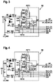
- FIG. 3 shows a schematic circuit diagram of a second exemplary embodiment of a protective device for the multi-line supply units of the present invention from FIGS. 1 and 2 , the protective device being connected to a power source.
- FIG. 4 shows a schematic circuit diagram of the protective device from FIG. 3 , which is connected to two power sources.
- FIG. 5 shows a schematic circuit diagram of a third exemplary embodiment of a protective device for the multi-line supply units of the present invention from FIGS. 1 and 2 .
- FIG. 6 shows a schematic circuit diagram of a third exemplary embodiment of a multi-line supply unit of the present invention for a vehicle control unit, including a fourth exemplary embodiment of a protective device.
- FIG. 7 shows a schematic circuit diagram of an exemplary embodiment of a hardware control unit for an evaluation and control unit of the multi-line supply unit of the present invention for a vehicle control unit from FIG. 6 .
- FIG. 8 shows a characteristic diagram of voltages during normal operation of the multi-line supply unit of the present invention for a vehicle control unit from FIG. 1 , including the protective device from FIG. 3 .
- FIG. 9 shows a characteristic diagram of different variables of the multi-line supply unit of the present invention for a vehicle control unit from FIGS. 1 and 2 , including the protective device from FIG. 4 ; the multi-line supply device having different steady components and being disturbed by a 1 kHz sinusoidal interference voltage.
- FIG. 10 shows a characteristic diagram of different variables of the multi-line supply unit of the present invention for a vehicle control unit from FIGS. 1 and 2 , including the protective device from FIG. 4 ; the multi-line supply device having different steady components.
- the depicted exemplary embodiments of a multi-line supply unit 1 A, 1 B, 1 C of the present invention for a vehicle control unit 2 each include at least two supply lines S 1 , S 2 , which are each connected to at least one vehicle voltage source B, B 1 , B 2 at the input and are joined at a common node KP at the output; and include a protective device 3 A, 3 B, 3 C, 3 D, which, in the at least two supply lines S 1 , S 2 , has at least one first damping diode Dvs 1 , Dvs 2 , respectively, that is looped into the at least two supply lines S 1 , S 2 , in the forward direction, between the at least one vehicle voltage source B, B 1 , B 2 and node KP.
- At least one switch element Svs 1 , Svs 2 is looped into each of the at least two supply lines S 1 , S 2 , respectively, in parallel with the at least one damping diode Dvs 1 , Dvs 2 , respectively; an evaluation and control unit 10 A, 10 B, 10 C measuring a line voltage VS 1 , VS 2 at the inputs of the at least two supply lines S 1 , S 2 , respectively, as well as a reverse-polarity-protected supply voltage VP at common node KP, and evaluating them.
- Evaluation and control unit 10 A, 10 B, 10 C controls switch elements Svs 1 , Svs 2 in the at least two supply lines S 1 , S 2 as a function of the evaluation, using corresponding control signals Svs 1 _CTL, Svs 2 _CTL.
- multi-line supply unit 1 A, 1 B, 1 C is implemented, in each instance, as a two-line supply unit having two supply lines S 1 , S 2 .
- multi-line supply unit 1 A, 1 B, 1 C may also include more than two supply lines S 1 , S 2 .
- first damping diodes Dvs 1 , Dvs 2 are used for static and/or dynamic reverse-polarity protection, power-supply security in the case of an open switch element Svs 1 , Svs 2 , and for feedback protection.
- switch elements Svs 1 , Svs 2 which are positioned in parallel with first damping diodes Dvs 1 , Dvs 2 , are used in supply lines S 1 , S 2 .
- Evaluation and control unit 10 A, 10 B, 10 C compares individual line voltages VS 1 , VS 2 to each other and/or to reverse-polarity-protected supply voltage VP and generates control signals Svs 1 _CTL, Svs 2 _CTL for switch elements Svs 1 , Svs 2 as a function of the comparisons, using a hardware control unit 12 A, 12 B, 12 C.
- hardware control unit 12 A, 12 B, 12 C uses connections to the two supply lines S 1 , S 2 via terminals VS 1 _IN, VS 2 _IN, as well as to common node KP via terminal VP_IN.
- Hardware control unit 12 A, 12 B, 12 C is powered by reverse-polarity-protected supply voltage VP and ground GND via terminals VP_IN and GND.
- evaluation and control unit 10 A, 10 B, 10 C closes switch elements Svs 1 , Svs 2 , using hardware control unit 12 A, 12 B, 12 C, if a difference between corresponding line voltage VS 1 , VS 2 and reverse-polarity-protected supply voltage VP at common node KP exceeds a predefined, first threshold value.
- Evaluation and control unit 10 A, 10 B, 10 C opens switch elements Svs 1 , Svs 2 , using hardware control unit 12 A, 12 B, 12 C, if the difference between corresponding line voltage VS 1 , VS 2 and reverse-polarity-protected supply voltage VP at common node KP falls below a predefined, second threshold value and/or becomes negative.
- a difference between the first threshold value and the second threshold value may be set, using a variable resistor Rhys in hardware control unit 12 A, 12 B, 12 C.
- a first switch element Svs 1 is closed, if a first control signal Svs 1 _CTL has a low value. If first control signal Svs 1 _CTL is processed in a special driver for first switch element Svs 1 , then, depending on the setting, either logical “high” or logical “low” voltage signals may close first switch element Svs 1 .
- first switch element Svs 1 remains open.
- a second switch element Svs 2 is closed, if a second control signal Svs 2 _CTL has a low value. If second control signal Svs 2 _CTL is processed in a special driver for second switch element Svs 2 , then, depending on the setting, either logical “high” or logical “low” voltage signals may close second switch element Svs 1 .
- the switch hysteresis advantageously prevents oscillation of switch elements Svs 1 , Svs 2 , since after the closing of corresponding switch element Svs 1 , Svs 2 , reverse-polarity-protected supply voltage VP increases to only slightly below line supply voltage VS 1 , VS 2 due to the low switch resistance.
- the switch hysteresis may either be fixedly selected for identical switch elements Svs 1 , Svs 2 .
- the hysteresis may be adjusted, using optional resistor Rhys.
- the internal resistances of switch elements Svs 1 , Svs 2 , the level of the line current in the supply direction, a desired stability of the switching decision, and a reverse-current detection level in corresponding supply line S 1 , S 2 are decisive for the adjustment.
- evaluation and control unit 10 A, 10 B, 10 C includes a processing unit 14 A, 14 B, 14 C, which checks the two supply lines S 1 , S 2 individually as a function of predefined conditions. In order to check the two supply lines S 1 , S 2 , processing unit 14 A, 14 B, 14 C generates corresponding control signals STR 1 _CTL, STR 2 _CTL and outputs them to hardware control unit 12 A, 12 B, 12 C.
- hardware control unit 12 A, 12 B, 12 C In response to control signals STR 1 _CTL, STR 2 _CTL, hardware control unit 12 A, 12 B, 12 C generates corresponding control signals Svs 1 _CTL, Svs 2 _CTL and outputs them to the two switch elements Svs 1 , Svs 2 or to their drivers.
- hardware control unit 12 A, 12 C and processing unit 14 A, 14 C of evaluation and control unit 10 A, 10 C are constructed as a unit and may be situated in the region of switch elements Svs 1 , Svs 2 or constructed as part of the control unit.
- hardware control unit 12 B and processing unit 14 B of evaluation and control unit 10 B are positioned separately from each other.
- hardware control unit 12 B is situated in the region of switch elements Svs 1 , Svs 2 , and processing unit 14 B is integrated in control unit 2 .
- a switching controller 2 . 1 of control unit 2 is coupled to common node KP of multi-line supply unit 1 B via a passive filter 20 .
- Passive filter 20 damps disturbances to the vehicle electrical system, in particular, sinusoidal interference over 5 kHz to 20 kHz, suppresses the conducted interference of switching controller 2 . 1 on the vehicle electrical system and ensures the supply of power to control unit 2 in the case of short-term, sudden drops in reverse-polarity-protected supply voltage VP.
- an advantageous exemplary embodiment 20 C of passive filter 20 is described with reference to FIG. 6 .
- the inputs of the two supply lines S 1 , S 2 are both connected to ground GND and damped via an RC element, which includes an ohmic resistor Rs 1 , Rs 2 and a capacitor Cs 1 , Cs 2 .
- the outputs of the two supply lines S 1 , S 2 are connected jointly to ground and damped at common node KP by an RC element, which includes an ohmic resistor RP and a capacitor CP.
- the exemplary embodiment represented in FIG. 4 only differs from the exemplary embodiment shown in FIG.
- protective device 3 B of multi-line supply unit 1 A is connected to only one vehicle power source B, which powers first supply line S 1 as a permanent vehicle voltage VB via a first line that is represented by a first ohmic line resistor Ri 1 and a first line inductor Li 1 , and which powers second supply line S 2 as a vehicle voltage VB, which is conducted by a second line that is represented by a second ohmic line resistor Ri 2 and a second line inductor Li 2 and is switched across an ignition lock ZS.
- first supply line S 1 as a permanent vehicle voltage VB via a first line that is represented by a first ohmic line resistor Ri 1 and a first line inductor Li 1
- second supply line S 2 as a vehicle voltage VB
- protective device 3 B of multi-line supply unit 1 A is connected to two vehicle power sources B 1 , B 2 .
- a first vehicle power source B 1 powers first supply line S 1 as a permanent, first vehicle voltage VB 1 via a first line, which is represented by a first ohmic resistor Ri 1 and a first line inductor Li 1
- a second vehicle power source B 2 powers second supply line S 2 as a second vehicle voltage VB 2 , which is conducted via a second line that is represented by a second ohmic line resistor Ri 2 and a second line inductor Li 2 , and which is connected across ignition lock ZS.
- the outputs of the depicted exemplary embodiments are each connected to ground GND and damped individually in front of common node KP, via an RC element, which includes, in each instance, an ohmic resistor Rs 11 , Rs 21 and a capacitor Cs 11 , Cs 21 .
- a connection to a vehicle power source B 1 , B 2 includes, in addition to ohmic resistor Ri 1 , Ri 2 , the line inductor Li 1 , Li 2 , as well, interference voltages on line voltages VS 1 , VS 2 and on reverse-polarity-protected supply voltage VP, due to the switching operations of switch elements Svs 1 , Svs 2 , may be compensated for by the RC elements; the interference voltages otherwise possibly being able to endanger the optimum control of switch elements Svs 1 , Svs 2 .
- the sizing of the RC elements is a function of line inductors Li 1 , Li 2 , as well as of the line currents of supply lines S 1 , S 2 .
- the characteristic diagram according to FIG. 8 shows a characteristic diagram of voltages during a simulation of normal operation of the multi-line supply unit 1 A of the present invention for a vehicle control unit 2 from FIG. 1 , including protective device 3 B from FIG. 3 .
- vehicle voltage VB is applied at time 1 , so that first line voltage VS 1 is greater than the difference of reverse-polarity-protected supply voltage VP and the set hysteresis, and that first switch element Svs 1 is closed.
- second line voltage VS 2 is less than the difference of reverse-polarity-protected supply voltage VP and the set hysteresis, which means that second switch element Svs 2 remains open.
- first supply line S 1 carries the total supply current IVP for the subsequent load RL, that is, a subsequent control unit. This results in first line voltage's VS 1 being less than vehicle voltage VB by the voltage drop V_Ri 1 at line resistor Ri of first supply line S 1 caused by supply current IVP.
- reverse-polarity-protected supply voltage VP is less than first line voltage VS 1 by the voltage drop V_Ri 1 across first switch element Svs 1 .
- the volume resistance of first switch element Svs 1 has a value of approximately 10 mOhm and is therefore very much less than the line resistance Ri1 of approximately 100 mOhm.
- the volume resistance of first switch element Svs 1 is a function of the size of the transistor used. Due to this, voltage drop V_Svs 1 across switch element Svs 1 is also very much less than voltage drop V_Ri 1 across line resistor Ri, which means that line resistor Ri of first supply line S 1 , and no longer the bypassed, first damping diode Dvs 1 , is decisive for the magnitude of reverse-polarity-protected supply voltage VP.
- ignition lock ZS that is, the ignition switch
- second line voltage VS 2 corresponds to vehicle voltage VB and is greater than the difference of reverse-polarity protected supply voltage VP and the set hysteresis. Therefore, second switch element Svs 2 in second supply line S 2 is also closed at time 2 .
- supply current IVP is provided via two supply lines S 1 , S 2 ; line resistors Ri 1 , Ri 2 of the supply lines, and no longer the reverse-polarity protection elements of protective device 3 B, being substantially responsible for the distribution of the current in supply lines S 1 , S 2 .
- first supply line S 1 provides 54% of supply current IVP
- second supply line S 2 supplies 46% of supply current IVP.
- the characteristic diagram of FIG. 9 shows different signal characteristics of multi-line supply unit 1 A of the present invention for a vehicle control unit 2 from FIG. 1 , including protective device 3 B from FIG. 4 ; the two vehicle voltages VB 1 , VB 2 , which are applied to the two supply lines S 1 , S 2 , having different d.c. voltage components and each being disturbed by a sinusoidal interference voltage.
- the interference voltage may be produced, for example, by a vehicle generator.
- first vehicle voltage VB 1 has a d.c. voltage component of 13.5 V and a first interference voltage having an amplitude of 4 V and a frequency of 1 kHz.
- Second vehicle voltage VB 2 includes a direct component of 11.5 V and a second interference voltage having an amplitude of 4 V and a frequency of 1 kHz; the first interference voltage and the second interference voltage having a phase shift of 90°.
- first vehicle voltage VB 1 is greater than second vehicle voltage VB 2
- first line voltage VS 1 is greater than the difference between reverse-polarity-protected supply voltage VP and the hysteresis.
- first switch element Svs 1 is closed. Due to this, voltage drop VS 1 -VP over first supply line S 1 is very low, and in spite of a high current Ivs 1 of approximately 14 A in first supply line S 1 , power loss P_Svs 1 of first switch element Svs 1 , at approximately 2 W, is extremely low.
- the power loss of a comparable damping diode not having a parallel switch element Svs 1 would lie between 7 W and 11 W.
- second vehicle voltage VB 2 is less than the difference between reverse-polarity-protected supply voltage VP and the hysteresis.
- second switch element Svs 2 is open. Due to this, no current IVS 2 flows in second supply line S 2 , and a blocking voltage is applied to first damping diode Dvs 2 of second supply line S 2 ; the blocking voltage preventing feedback from first supply line S 1 into second supply line S 2 . Consequently, the supply of power to control unit 2 at time 1 occurs exclusively via first supply line S 1 .
- Voltage drop VS 2 -VP over the second supply line corresponds to voltage drop VS 1 -VP over first supply line S 1 and, at 50 mV, is approximately three times smaller than voltage drop VS 1 -VP over first supply line S 1 at time 1 .
- the characteristic diagram of FIG. 10 shows different signal characteristics of multi-line supply unit 1 A of the present invention for a vehicle control unit 2 from FIG. 1 , including protective device 3 B from FIG. 4 ; the two vehicle voltages VB 1 , VB 2 , which are applied to the two supply lines S 1 , S 2 , having different d.c. voltage components and not being disturbed by interference voltages.
- first vehicle voltage VB 1 includes a d.c. voltage component of 13.5 V
- second vehicle voltage VB 2 includes a d.c. voltage component of 12.5 V.
- first vehicle voltage VB 1 is greater than second vehicle voltage VB 2 at time 1 .
- line resistances Ri 1 , Ri 2 of supply lines S 1 , S 2 are crucial to the current distribution of high-current control units, since internal impedances of control unit 2 make almost no difference due to the reduction in power loss.
- multi-line supply unit 1 A, 1 B, 1 C according to the present invention is that in addition to the redundancy for signaling a power supply fault, with the reliable assumption of control by the driver over an at least semiautonomous vehicle function, a permanent reduction of power loss in protective device 3 A, 3 B, 3 C, 3 D is also achieved due to the current distribution.
- a permanent reduction of power loss in protective device 3 A, 3 B, 3 C, 3 D is also achieved due to the current distribution.
- voltage drops VS 1 -Vp, VS 2 -Vp over supply lines S 1 , S 2 are extremely small.
- a field-effect transistor FET 1 , FET 2 forms first damping diode Dvs 1 , Dvs 2 and corresponding switch element Svs 1 , Svs 2 in the two supply lines S 1 , S 2 .
- field-effect transistors FET 1 , FET 2 are each constructed as a p-channel power MOSFET.
- a second damping diode Dzs 1 , Dzs 2 is in the two supply lines S 1 , S 2 , parallel to first damping diode Dvs 1 , Dvs 2 and to switch element Svs 1 , Svs 2 .
- Second damping diodes Dzs 1 , Dzs 2 protect switch elements Svs 1 , Svs 2 and reduce a pulse loading of switch elements Svs 1 , Svs 2 .
- switch elements Svs 1 , Svs 2 may be protected from an ISO pulse loading, which may generate voltages of over 40 V across switch elements Svs 1 , Svs 3 .
- second damping diodes Dzs 2 , Dzs 2 are configured as suppressor diodes (TSV) having an avalanche voltage in the range of 24 V to 40 V.
- a reverse-polarity-protected supply voltage VP having a value of approximately 12V is applied to common node KP for a moment. This produces a corresponding, peak line voltage VS 1 , VS 2 of approximately ⁇ 100 V.
- Additional, second damping diodes Dzs 1 , Dzs 2 may be omitted, if the MOSFET's used have a sufficient and specific, periodic avalanche energy. In this manner, the static reverse-polarity safety of control unit 2 against voltages up to 20 V is ensured, as is the active measures against the negative pulse loading.
- the outputs of the two supply lines S 1 , S 2 are jointly connected to ground GND at a common node KP, via a third damping diode Dzp, which reduces a positive pulse loading of the two supply lines S 1 , S 2 .
- the outputs of the two supply lines S 1 , S 2 are each individually connected to ground in front of common node KP, via a third damping diode Dzs 11 , Dzs 21 , which reduces a positive pulse loading of the two supply lines S 1 , S 2 .
- Third damping diodes Dzp, Dzs 11 , Dzs 21 are used to protect against positive ISO pulses, including a load dump. If a positive pulse load occurs in a supply line S 1 , S 2 , then pulses over 30 V are clamped or limited at common node KP by third damping diodes Dzp, Dzs 11 , Dzs 21 .
- the avalanche voltage of third damping diode Dzp, Dzs 11 , Dzs 21 may be selected to be in the range of 30 V to 42 V.
- Third damping diodes Dzp, Dzs 11 , Dzs 21 produce cost-effective solutions having MOSFET's as switch elements Svs 1 , Svs 2 and allow asymmetric clamping or limiting of negative supply pulses by the second damping diodes Dzs 1 , Dzs 2 , and of positive supply pulses by third damping diodes Dzp, Dzs 11 , Dzs 21 , which means that size or absorption power of the negative clamping elements may be decoupled from that of the positive clamping elements.
- the unidirectional clamping at common node KP unites increased protection from polarity reversal in the case of a defect of a line switch, with the objective of tripping the line circuit breaker before damage occurs in control unit 2 .
- passive filter 20 is constructed as a multi-line T filter 20 C.
- a first filter inductor LT 1 , LT 2 is looped into the two supply lines S 1 , S 2 , between switch element Svs 1 , Svs 2 and common node KP.
- a common, second filter inductor LT is looped in between common node KP and a filter output VZP.
- filter coils LT, LT 1 , LT 2 a filter capacitor CT, as well as an output capacitor Cout, filter 20 C may be adapted to the following switching controller 2 .
- filter 20 C has a buffer capacitor C ⁇ CT, which is constructed, for example, as a hybrid-polymer electrolytic capacitor having a very small ESR.
- Buffer capacitor C ⁇ CT is coupled to common node KP via an ohmic limiting resistor R ⁇ CT, which has a value between 0.1 and 1 Ohm and limits a peak current.
- buffer capacitor C ⁇ CT is connected to filter output VZP via a coupling diode D ⁇ CT.
- Coupling diode D ⁇ CT ensures rapid and low-resistance buffering of the input voltage of the switching converter in the case of a temporary voltage interruption of first vehicle voltage VB 1 and/or of the second vehicle voltage.
- Coupling diode D ⁇ CT is preferably implemented as a Schottky diode.
- Multi-line T filter 20 C advantageously allows multi-line supply unit 1 C to be coupled directly to switching controller 2 . 1 of control unit 2 .
- Passive filter 20 C damps disturbances to the vehicle electrical system, in particular, high-frequency sinusoidal interference from over 5 kHz to 20 kHz, suppresses the conducted interference of switching controller 2 . 1 on the vehicle electrical system and ensures the supply of power to control unit 2 in the case of sudden voltage drops in supply lines S 1 , S 2 .
- the first filter inductors LT 1 , LT 2 integrated in supply lines S 1 , S 2 produce a time delay in the build-up of a feedback current from supply line S 1 to supply line S 2 , and vice versa.
- reverse-polarity-protected supply voltage VP may be measured after the inductive coupling, which means that an additional hysteresis is produced due to ohmic coil resistor RT 1 , RT 2 .
- a short circuit to ground occurs in a supply line S 1 , S 2 .
- the limited switching rate of the checking of line voltage VS 1 , VS 2 against reverse-polarity-protected supply voltage VP at common node KP and the limited opening speed of switch elements Svs 1 , Svs 2 feedback of the energy stored in buffer capacitor C ⁇ CT may not be prevented completely, but may be improved markedly over the exemplary embodiment of multi-line supply unit 1 B represented in FIG. 2 .
- Hardware control unit 12 A, 12 B, 12 C or parts of hardware control unit 12 A, 12 B, 12 C are switched “on” or “off” via an N_SL input, to which a sleep-mode control signal N_SL is applied.
- N_SL a sleep-mode control signal
- the control lines of control signals STR 1 _CTL, STR 2 _CTL are led to hardware control unit 10 A, 10 B, 10 C.
- the monitoring processing unit 14 A, 14 B, 14 C may open switch elements Svs 1 , Svs 2 temporarily. Due to this, in response to a line interruption in a supply line S 1 , S 2 , line voltage VS 1 , VS 2 falls below a predefined threshold value. This information is used for detecting faults in the redundant supply of power to the control units, with the object of giving the driver control again over the at least semiautonomous function in a timely manner or regaining the attention of the driver in time.
- supply current IVP is concentrated on the supply line S 1 , S 2 to be checked, it may therefore be checked if, under load at the current-carrying supply line S 1 , S 2 to be checked, a sufficiently high line voltage VS 1 , VS 2 is still present at the input.
- control unit 2 If control unit 2 is in sleep mode, then sleep mode control signal N_SL has the low logical voltage level, and hardware control unit 12 A, 12 B, 12 C absorbs only a very low supply current IVP at terminal VP_IN, which is considerably lower than 10 ⁇ A. In the same manner, no significant current flows into terminals VS 1 _IN, VS 2 _IN, as well. In other words, the current flowing into the terminals is also very much less than 10 ⁇ A. In addition, in sleep mode, switch elements Svs 1 , Svs 2 are in their “default state,” that is, open. Control unit 1 , itself, is not active in sleep mode and absorbs only a small supply current from common node KP, which is less than 100 ⁇ A. Thus, the voltage drop, which first damping diodes may cause, is insignificant. If control unit 2 is awoken, then sleep-mode control signal N_SL changes to the high logical level, and hardware control unit 12 A, 12 B, 12 C is activated.
- the field-effect transistors FET 1 , FET 2 implemented in the form of p-channel power MOSFET's conduct in the forward direction via bulk diodes Dsv 1 , Dsv 2 , between the drain and the source.
- These field effect transistors FET 1 , FET 2 are controlled, using a positive source-gate voltage, which is synonymous with connecting the respective gate to ground via control lines of control signals Svs 1 _CTL, Svs 2 _CTL.
- field-effect transistors FET 1 , FET 2 allow, as a rule, a maximum source-gate voltage of 20 V and, in order to increase the switching speed, the source-gate voltages are each limited to a value of, for example, 5.1 V by a Zener diode ZD 1 _ 1 , ZD 2 _ 1 situated in hardware control unit 10 C.
- a source-gate bleeder resistor R 1 _ 9 , R 2 _ 9 (e.g., 100 kOhm) is positioned in parallel with this Zener diode ZD 1 _ 1 , ZD 2 _ 1 , respectively, in order to be able to reliably block corresponding switch element Svs 1 , Svs 2 in sleep mode.
- control lines of control signals Svs 1 _CTL, Svs 2 _CTL are constructed to be switchable by sleep-mode control signal N_SL via transistors T 1 _ 3 , T 2 _ 3 .
- Resistors R 1 _ 6 , R 2 _ 6 (e.g., 5.1 kOhm) are used for limiting current in the control lines of control signals Svs 1 _CTL, Svs 2 _CTL in the case of an active control unit 2 , which allows a voltage VS 11 , VS 21 in the range of 5 V to 36 V in front of first filter inductors LT 1 , LT 2 _and, therefore, at the terminals of hardware control unit 10 C, as well.
- Resistors R 1 _ 7 (e.g., 23.7 kOhm), R 1 _ 8 (e.g., 51.1 kOhm), R 2 _ 7 (e.g., 23.7 kOhm), R 2 _ 8 (e.g., 51 . 1 kOhm) form the base dividers for NPN control transistors T 1 _ 3 , T 2 _ 3 .
- Line voltages VS 1 , VS 2 are acquired at hardware control unit 10 C via terminals VS 1 _IN, VS 2 _IN and are forwarded, via switchable transistors T 1 _ 11 , T 2 _ 11 , to corresponding voltage dividers R 1 _ 13 (e.g., 75 kOhm), R 1 _ 14 (e.g., 8.25 kOhm), and R 2 _ 13 (e.g., 75 kOhm), R 2 _ 14 (e.g., 8.25 kOhm), respectively.
- Divided signals VS 1 _ADC, VS 2 _ADC are forwarded to processing unit 14 C.
- PNP transistors T 1 _ 11 , T 2 _ 11 are switchable, in order not to generate any measuring-divider current to ground from line voltages VS 1 , VS 2 .
- these transistors T 1 _ 11 , T 2 _ 11 are switched through NPN control transistors T 1 _ 10 , T 2 _ 10 with the aid of sleep-mode control signal N_SL.
- Sleep-mode control signal N_SL has a low logical level in sleep mode and a high logical level in normal mode.
- Resistors R 1 _ 15 , R 1 _ 16 and R 2 _ 15 , R 2 _ 16 (e.g., 23.7 kOhm, 51.1 kOhm and 23.7 kOhm, 51.1 kOhm, respectively) form a base voltage divider of NPN control transistors T 1 _ 10 , T 2 _ 10 , respectively.
- supply lines S 1 , S 2 are interconnected via first filter inductors LT 1 , LT 2 _and generate reverse-polarity-protected supply voltage VP at common node KP.
- Reverse-polarity-protected supply voltage VP is supplied to hardware control unit 10 C at terminal VP_IN.
- a positive supply voltage is supplied to comparators CMP_ 1 , CMP_ 2 at corresponding, positive supply pins, via a PNP switching transistor T 12 _ 1 and a low-pass filter R 12 _ 1 , C 12 _ 1 (e.g., 10 Ohm, 10 ⁇ F).
- this switching transistor T 12 _ 1 is also controllable by sleep-mode control signal N_SL.
- a resistor R 12 _ 4 (e.g., 40.2 kOhm) is used for limiting current in the control path of switching transistor T 12 _ 1 .
- a resistor R 12 _ 3 (e.g., 51.1 kOhm) is used as a base-emitter bleeder resistor of transistor T 12 _ 1 .
- Resistors R 12 _ 5 , R 12 _ 6 (e.g., 23.7 kOhm, 51.1 kOhm) form a base divider of NPN control transistor T 12 _ 2 .
- Reverse-polarity-protected supply voltage VP of coupled supply lines S 1 , S 2 is applied to negative inputs of comparators CMP_ 1 , CMP_ 2 via series resistors R 1 _ m , R 2 _ m (e.g., 100 ⁇ ).
- Line voltages VS 1 , VS 2 at the inputs of supply lines S 1 , S 2 are applied to positive inputs of comparators CMP_ 1 , CMP_ 2 via terminals VS 1 _IN, VS 2 _IN and series resistors R 1 _ p , R 2 _ p (e.g., 5.1 kOhm).
- comparators CMP_ 1 , CMP_ 2 are protected by unidirectional Zener diodes ZD 1 _ 10 , ZD 2 _ 10 , respectively, which allow, for example, a clamping voltage of 27 V.
- the clamping voltages of Zener diodes ZD 1 _ 10 , ZD 2 20 should be selected to lie below the clamping voltages of damping diodes Dzs 11 , Dzs 21 , Dzp, in order that at a high, positive pulse loading in the vehicle electrical system, switch elements Svs 1 , Svs 2 of supply lines S 1 , S 2 are forcibly opened and the coupling of control unit 2 only takes place via first and second damping diodes Dvs 1 , Dvs 2 , Dzs 1 , Dzs 2 of the two supply lines S 1 , S 2 . This allows the risk to be reduced in the case of a load dump.
- the comparators CMP_ 1 , CMP_ 2 used preferably have a “common mode range,” which may lie, for example, 44 V over an electric potential at the grounded connection of comparators CMP_ 1 , CMP_ 2 , irrespective of the positive supply voltage of the comparators.
- PNP switching transistors T 1 _ 1 , T 2 _ 1 may be activated by control signals STR 1 _CTL, STR 2 _CTL of processing unit 14 with the aid of NPN control transistors T 1 _ 2 , T 2 _ 2 and, therefore, may force a transition of supply lines S 1 , S 2 to reverse-polarity-protected operation via first damping diodes Dvs 1 , Dvs 2 .
- Resistors R 1 _ 2 , R 2 _ 2 are used to limit current during the activation.
- Resistors R 1 _ 4 , R 1 _ 5 and R 2 _ 4 , R 2 _ 5 are used as base voltage dividers of NPN control transistors T 1 _ 2 , T 2 _ 2 , respectively.
- a reference current is determined by reference voltage VREF and optional resistor R 12 _Hy. This is supplied to a current mirror T 12 _ 3 .
- Mirror currents IREF are decoupled by transistors T 12 _ 4 , T 12 _ 5 and supplied to the negative inputs of comparators CMP_ 1 , CMP_ 2 .
- An adjustable hysteresis of comparators CMP_ 1 , CMP_ 2 is formed together with resisters R 1 _ m , R 2 _ m.
- sleep-mode control signal N_SL and control signals STR 1 _CTL, STR 2 _CTL each have the low logical level, then hardware control unit 10 C is not active and no current or an irrelevantly small amount of current in the ⁇ A range is consumed at terminals VS 1 _IN, VS 2 _IN, VS 11 _IN, VS 21 _IN, VP_IN of hardware control unit 10 C.
- field-effect transistors FET 1 , FET 2 are switched off, and line voltages VS 1 , VS 2 are protected from polarity reversal by first damping diodes Dsv 1 , Dsv 2 and/or parallelly situated, unidirectional, second damping diodes Dzs 1 , Dzs 2 and relayed to passive filter 20 C; feedback from one supply line S 1 , S 2 to the other supply line S 1 , S 2 not being possible.
- a switch is made to normal operation having a first line voltage VS 1 of 14 V, a second line voltage VS 2 of 14 V, a first line resistance Ri 1 of 200 m ⁇ ), a second line resistance Ri 2 of 200 m ⁇ ) and sleep-mode control signal N_SL on a high logical voltage level, and control signals STR 1 _CTL, STR 2 _CTL on a low logical voltage level, then the voltage at the negative input of first comparator CMP_ 1 is less than line voltage VS 1 at the positive input of first comparator CMP_ 1 by the voltage drop between first line voltage VS 1 and reverse-polarity-protected supply voltage VP, plus a first hysteresis.
- the voltage at the negative input of second comparator CMP_ 2 is less than line voltage VS 2 at the positive input of second comparator CMP_ 2 by the voltage drop between first line voltage VS 1 and reverse-polarity-protected supply voltage VP, plus a second hysteresis. Due to this, the outputs of the two comparators CMP_ 1 , CMP_ 2 are blocked. Thus, the PNP switching transistors T 1 _ 1 , T 2 _ 1 for controlling field-effect transistors FET 1 , FET 2 are blocked, as well. Since sleep-mode control signal N_SL is at a high logical voltage level during normal operation, control transistors T 1 _ 3 , T 2 _ 3 are conductive.
- line resisters Ri 1 , Ri 2 are responsible for the current distribution in supply lines S 1 , S 2 , if vehicle voltages VB 1 , VB 2 are of equal magnitude.
- a line voltage VS 1 , VS 2 at the inputs of the at least two supply lines S 1 , S 2 , respectively, is measured and evaluated, and a reverse-polarity-protected voltage VP at common node KP is measured and evaluated.
- switch elements Svs 1 , Svs 2 in the at least two supply lines S 1 , S 2 are controlled as a function of the evaluation, using corresponding control signals Svs 1 _CTL, Svs 2 _CTL.
- processing unit 14 C may compare individual line voltages VS 1 , VS 2 to each other and/or to reverse-polarity-protected supply voltage VP and generate control signals Svs 1 _CTL, Svs 2 _CTL for the at least one switch element Svs 1 , Svs 2 as a function of the comparisons, using a hardware control unit 12 A, 12 B, 12 C.
- the at least two supply lines S 1 , S 2 may be checked individually during operation as a function of predefined conditions.
- the at least two supply lines S 1 , S 2 may be checked individually by processing unit 14 C at predefined intervals, and/or when a voltage difference between line voltages VS 1 , VS 2 exceeds a predefined magnitude. Without these checking functions, line voltage S 1 , S 2 of functional supply line S 1 , S 2 may also be applied to the input of interrupted supply line S 1 , S 2 due to the coupling at common node KP and conductive switch elements Svs 1 , Svs 2 and, therefore, may not be detected by the voltage check.
- processing unit 14 C may open field-effect transistors FET 1 , FET 2 , using control signals STR 1 _CTL, STR 2 _CTL, which are set to a high logical level, which means that an interrupted supply of power to the lines may be detected.
- processing unit 14 C may open the at least one switch element Svs 1 , Svs 2 of the supply line S 1 , S 2 to be checked, and the reactions of corresponding line voltage VS 1 , VS 2 and reverse-polarity-protected supply voltage VP at common node KP may be measured and evaluated.
- a line interruption in the supply line S 1 , S 2 to be checked may be detected, if, in response to an open switch element Svs 1 , Svs 2 , corresponding line voltage VS 1 , VS 2 is below a predefined, minimum limiting value in the range of 0 to 6 V.
- first control signal STR 1 _CTL is set to the low logical voltage level
- second control signal STR 2 _CTL is set to the high logical voltage level, in order to check second supply line S 2 for a line interruption.
- second supply line S 2 experiences a decrease in voltage around the first damping diode Dvs 2 and/or second damping diode Dzvs 2 now active, supply current IVP is concentrated on first supply line S 1 .
- first line voltage VS 1 is acquired as first voltage VS 1 _ADC
- second line voltage VS 2 is acquired as second voltage VS 2 _ADC
- second voltage VS 2 _ADC corresponds approximately to second vehicle voltage VB 2
- line current Isv 2 is not flowing in second supply line S 2 .
- First voltage VS 1 _ADC corresponds to first line voltage VS 1 at a maximum loading.
- a line interruption to second supply line S 2 may be detected, if a voltage markedly lower than the vehicle voltage VB 2 to be expected is applied to the input of second supply line S 2 .
- first control signal STR 1 _CTL may be set to the high logical voltage level
- second control signal STR 2 _CTL may be set to the low logical voltage level, in order to check first supply line S 1 .
- first line voltage VS 1 is acquired as first voltage VS 1 _ADC and second line voltage VS 2 is acquired as second voltage VS 2 _ADC
- first line voltage VS 1 _ADC corresponds approximately to first vehicle voltage VB 1
- line current Isv 1 is not flowing in first supply line S 1
- Second voltage VS 2 _ADC corresponds to second line voltage VS 2 at a maximum loading.
- a line interruption to first supply line S 1 may be detected, if a voltage markedly lower than the first vehicle voltage VB 1 to be expected is applied to the input of first supply line S 1 .
- processing unit 14 C may deduce the quality of supply line S 1 , S 2 and provide a maintenance information item.
- vehicle voltages VB 1 , VB 2 of processing unit 14 C may also be provided by central vehicle systems over different communication paths (Ethernet, FlexRay, CAN, LIN). In this connection, poor quality may be detected due to the calculated internal resistance's exceeding a predefined limiting value. The internal resistance may increase, that is, become worse, over the service life, for example, due to corrosion at the contact points.
- Processing unit 14 C may then generate a warning signal and output it via an acoustic and/or optical output unit, if a line interruption and/or a problem and/or poor quality is detected in at least one of the two supply lines S 1 , S 2 . Additionally, or as an alternative, processing unit 14 C may store the warning message and output it at a later time via a diagnostic interface. In this manner, the specific, at least semiautonomous function may be returned to the driver again, and/or rapid service may be initiated without there being an urgent necessity for it, since due to the redundant, two-line power supply, no unwanted functional limitation occurs initially.
Landscapes
- Engineering & Computer Science (AREA)
- Power Engineering (AREA)
- Physics & Mathematics (AREA)
- General Physics & Mathematics (AREA)
- Automation & Control Theory (AREA)
- Mechanical Engineering (AREA)
- Testing Of Short-Circuits, Discontinuities, Leakage, Or Incorrect Line Connections (AREA)
- Charge And Discharge Circuits For Batteries Or The Like (AREA)
- Electronic Switches (AREA)
- Direct Current Feeding And Distribution (AREA)
- Emergency Protection Circuit Devices (AREA)
- Dc-Dc Converters (AREA)
Applications Claiming Priority (3)
| Application Number | Priority Date | Filing Date | Title |
|---|---|---|---|
| DE102017217003.4A DE102017217003A1 (de) | 2017-09-26 | 2017-09-26 | Mehrstrangversorgungseinheit für ein Fahrzeugsteuergerät |
| DE102017217003.4 | 2017-09-26 | ||
| PCT/EP2018/072116 WO2019063186A1 (de) | 2017-09-26 | 2018-08-15 | Mehrstrangversorgungseinheit für ein fahrzeugsteuergerät |
Publications (2)
| Publication Number | Publication Date |
|---|---|
| US20210159694A1 US20210159694A1 (en) | 2021-05-27 |
| US11177655B2 true US11177655B2 (en) | 2021-11-16 |
Family
ID=63350529
Family Applications (1)
| Application Number | Title | Priority Date | Filing Date |
|---|---|---|---|
| US16/647,190 Active US11177655B2 (en) | 2017-09-26 | 2018-08-15 | Multi-line supply unit for a vehicle control unit |
Country Status (8)
| Country | Link |
|---|---|
| US (1) | US11177655B2 (ko) |
| EP (1) | EP3688854A1 (ko) |
| JP (1) | JP6993514B2 (ko) |
| KR (1) | KR102568231B1 (ko) |
| CN (1) | CN111133650B (ko) |
| DE (1) | DE102017217003A1 (ko) |
| MX (1) | MX2020003025A (ko) |
| WO (1) | WO2019063186A1 (ko) |
Cited By (1)
| Publication number | Priority date | Publication date | Assignee | Title |
|---|---|---|---|---|
| US20220147079A1 (en) * | 2020-11-06 | 2022-05-12 | Aisin Corporation | Sensor module |
Families Citing this family (4)
| Publication number | Priority date | Publication date | Assignee | Title |
|---|---|---|---|---|
| DE102020113629A1 (de) | 2020-05-20 | 2021-11-25 | Bayerische Motoren Werke Aktiengesellschaft | Elektrischer Verbraucher und Verfahren zur Anbindung eines elektrischen Verbrauchers an ein elektrisches Bordnetz |
| DE102020115461A1 (de) * | 2020-06-10 | 2021-12-16 | Auto-Kabel Management Gmbh | Kraftfahrzeugbordnetzschalter, Kraftfahrzeugbordnetz und Verfahren zum Betreiben eines Kraftfahrzeugbordnetzschalters |
| CN114301028B (zh) | 2021-12-29 | 2023-09-29 | 视涯科技股份有限公司 | 一种过流保护电路及显示装置 |
| EP4435991A1 (en) * | 2023-03-21 | 2024-09-25 | Aptiv Technologies AG | Electrical power supply |
Citations (19)
| Publication number | Priority date | Publication date | Assignee | Title |
|---|---|---|---|---|
| JPH03243119A (ja) | 1990-02-19 | 1991-10-30 | Nippon Telegr & Teleph Corp <Ntt> | オア回路 |
| JPH05328606A (ja) | 1992-05-18 | 1993-12-10 | Kokusai Electric Co Ltd | 2重化直流電源回路 |
| JPH0775348A (ja) | 1993-08-31 | 1995-03-17 | Toshiba Corp | 燃料電池装置 |
| JPH09140065A (ja) | 1995-11-10 | 1997-05-27 | Sony Corp | 並列使用の2次電池装置 |
| JPH09261861A (ja) | 1996-03-22 | 1997-10-03 | Omron Corp | 逆流防止装置、整流装置および太陽光発電システム |
| US5757099A (en) * | 1996-03-01 | 1998-05-26 | Wisconsin Alumni Research Foundation | Hybrid parallel active/passive filter system with dynamically variable inductance |
| JP2001053597A (ja) | 1999-08-06 | 2001-02-23 | Matsushita Electric Works Ltd | 照度センサおよび電子式自動点滅器 |
| US20060002043A1 (en) * | 2004-04-30 | 2006-01-05 | Disalvo Nicholas L | Overcurrent protection for circuit interrupting devices |
| JP2007082306A (ja) | 2005-09-13 | 2007-03-29 | Hitachi Ltd | 電源供給装置 |
| JP2009077510A (ja) | 2007-09-20 | 2009-04-09 | Hitachi Ltd | 電解コンデンサの充放電回路 |
| JP2009159222A (ja) | 2007-12-26 | 2009-07-16 | Sanken Electric Co Ltd | スイッチ装置 |
| JP2010004617A (ja) | 2008-06-18 | 2010-01-07 | Mitsubishi Electric Corp | 車載電子制御装置の電源異常検出回路 |
| US7768244B2 (en) | 2006-12-18 | 2010-08-03 | Agence Spatiale Europeene | Power-maximizing electrical energy generation system |
| EP2413450A2 (en) | 2010-07-12 | 2012-02-01 | Hamilton Sundstrand Corporation | Electric power generating and distribution system comprising a decoupling filter and a solid state power controller |
| US20120228943A1 (en) * | 2010-10-15 | 2012-09-13 | Sanyo Electric Co., Ltd. | Electric power supply system |
| JP2013066321A (ja) | 2011-09-20 | 2013-04-11 | Hitachi Automotive Systems Ltd | 車載用制御装置 |
| WO2013060604A2 (en) | 2011-10-28 | 2013-05-02 | Sma Solar Technology Ag | Inverter with bridgeable reverse current protection device |
| JP2013517751A (ja) | 2010-01-13 | 2013-05-16 | フェニックス コンタクト ゲーエムベーハー ウント コムパニー カーゲー | 対称な電流経路を伴う冗長モジュール |
| JP2016071427A (ja) | 2014-09-26 | 2016-05-09 | 株式会社オートネットワーク技術研究所 | 車載機 |
Family Cites Families (3)
| Publication number | Priority date | Publication date | Assignee | Title |
|---|---|---|---|---|
| CN102496923B (zh) * | 2011-11-14 | 2016-10-19 | 株洲南车时代电气股份有限公司 | 一种防反接保护的输入电路 |
| DE102012212123B4 (de) * | 2012-07-11 | 2016-05-19 | Continental Automotive Gmbh | Vorrichtung zur Diagnose einer Schaltungsanordnung |
| CN103441486A (zh) * | 2013-08-14 | 2013-12-11 | 上海华兴数字科技有限公司 | 一种大电流电源防反接保护电路 |
-
2017
- 2017-09-26 DE DE102017217003.4A patent/DE102017217003A1/de active Pending
-
2018
- 2018-08-15 KR KR1020207011754A patent/KR102568231B1/ko active Active
- 2018-08-15 JP JP2020537845A patent/JP6993514B2/ja active Active
- 2018-08-15 US US16/647,190 patent/US11177655B2/en active Active
- 2018-08-15 WO PCT/EP2018/072116 patent/WO2019063186A1/de not_active Ceased
- 2018-08-15 MX MX2020003025A patent/MX2020003025A/es unknown
- 2018-08-15 EP EP18759071.6A patent/EP3688854A1/de active Pending
- 2018-08-15 CN CN201880062687.8A patent/CN111133650B/zh active Active
Patent Citations (19)
| Publication number | Priority date | Publication date | Assignee | Title |
|---|---|---|---|---|
| JPH03243119A (ja) | 1990-02-19 | 1991-10-30 | Nippon Telegr & Teleph Corp <Ntt> | オア回路 |
| JPH05328606A (ja) | 1992-05-18 | 1993-12-10 | Kokusai Electric Co Ltd | 2重化直流電源回路 |
| JPH0775348A (ja) | 1993-08-31 | 1995-03-17 | Toshiba Corp | 燃料電池装置 |
| JPH09140065A (ja) | 1995-11-10 | 1997-05-27 | Sony Corp | 並列使用の2次電池装置 |
| US5757099A (en) * | 1996-03-01 | 1998-05-26 | Wisconsin Alumni Research Foundation | Hybrid parallel active/passive filter system with dynamically variable inductance |
| JPH09261861A (ja) | 1996-03-22 | 1997-10-03 | Omron Corp | 逆流防止装置、整流装置および太陽光発電システム |
| JP2001053597A (ja) | 1999-08-06 | 2001-02-23 | Matsushita Electric Works Ltd | 照度センサおよび電子式自動点滅器 |
| US20060002043A1 (en) * | 2004-04-30 | 2006-01-05 | Disalvo Nicholas L | Overcurrent protection for circuit interrupting devices |
| JP2007082306A (ja) | 2005-09-13 | 2007-03-29 | Hitachi Ltd | 電源供給装置 |
| US7768244B2 (en) | 2006-12-18 | 2010-08-03 | Agence Spatiale Europeene | Power-maximizing electrical energy generation system |
| JP2009077510A (ja) | 2007-09-20 | 2009-04-09 | Hitachi Ltd | 電解コンデンサの充放電回路 |
| JP2009159222A (ja) | 2007-12-26 | 2009-07-16 | Sanken Electric Co Ltd | スイッチ装置 |
| JP2010004617A (ja) | 2008-06-18 | 2010-01-07 | Mitsubishi Electric Corp | 車載電子制御装置の電源異常検出回路 |
| JP2013517751A (ja) | 2010-01-13 | 2013-05-16 | フェニックス コンタクト ゲーエムベーハー ウント コムパニー カーゲー | 対称な電流経路を伴う冗長モジュール |
| EP2413450A2 (en) | 2010-07-12 | 2012-02-01 | Hamilton Sundstrand Corporation | Electric power generating and distribution system comprising a decoupling filter and a solid state power controller |
| US20120228943A1 (en) * | 2010-10-15 | 2012-09-13 | Sanyo Electric Co., Ltd. | Electric power supply system |
| JP2013066321A (ja) | 2011-09-20 | 2013-04-11 | Hitachi Automotive Systems Ltd | 車載用制御装置 |
| WO2013060604A2 (en) | 2011-10-28 | 2013-05-02 | Sma Solar Technology Ag | Inverter with bridgeable reverse current protection device |
| JP2016071427A (ja) | 2014-09-26 | 2016-05-09 | 株式会社オートネットワーク技術研究所 | 車載機 |
Non-Patent Citations (1)
| Title |
|---|
| International Search Report for PCT/EP2018/072116, dated Nov. 29, 2018. |
Cited By (1)
| Publication number | Priority date | Publication date | Assignee | Title |
|---|---|---|---|---|
| US20220147079A1 (en) * | 2020-11-06 | 2022-05-12 | Aisin Corporation | Sensor module |
Also Published As
| Publication number | Publication date |
|---|---|
| KR102568231B1 (ko) | 2023-08-23 |
| EP3688854A1 (de) | 2020-08-05 |
| WO2019063186A1 (de) | 2019-04-04 |
| US20210159694A1 (en) | 2021-05-27 |
| DE102017217003A1 (de) | 2019-03-28 |
| CN111133650A (zh) | 2020-05-08 |
| JP2020535785A (ja) | 2020-12-03 |
| KR20200060740A (ko) | 2020-06-01 |
| CN111133650B (zh) | 2022-09-27 |
| JP6993514B2 (ja) | 2022-02-15 |
| MX2020003025A (es) | 2020-07-22 |
Similar Documents
| Publication | Publication Date | Title |
|---|---|---|
| US11177655B2 (en) | Multi-line supply unit for a vehicle control unit | |
| US8487633B2 (en) | Fault detection of electric consumers in motor vehicles | |
| CN108068729B (zh) | 包括具有同时开关状态检测功能的多重模拟开关监测系统的车辆 | |
| US10340908B2 (en) | Half-bridge driver fault diagnostic system and method | |
| US11611205B2 (en) | Triggering circuit and electronic fuse device incorporating the same | |
| JP6784918B2 (ja) | レギュレータ用半導体集積回路 | |
| US10618479B2 (en) | Controller for a multi-voltage on-board power supply system in a vehicle | |
| US10090666B2 (en) | Circuit architectures for protecting against PoDL wire faults | |
| US20160294181A1 (en) | Overvoltage protection for a motor vehicle electrical system in the event of load shedding | |
| US20110068849A1 (en) | Active Monostable Positive Transient Protection Circuit for a Capacitive Load | |
| JPH0858556A (ja) | 自動車用電子制御装置及び自動車用電子制御装置を保護する方法 | |
| US20120126782A1 (en) | Low voltage electronic module interface | |
| US20190308572A1 (en) | Multi-voltage control device for a motor vehicle, motor vehicle and operating method for the control device | |
| US20220278524A1 (en) | Power supply system with protection against current variations | |
| US20240201242A1 (en) | Device for monitoring a power distributor of a motor vehicle | |
| EP1787373A1 (en) | Method and apparatus for generator control | |
| KR102522948B1 (ko) | 차량용 안전 유닛을 위한 활성화 전압의 제공을 위한 장치 및 방법, 그리고 안전 장치 | |
| KR101636291B1 (ko) | 정션박스의 전원 공급 배선 장애 검출 장치 및 그 방법 | |
| US9985625B2 (en) | Method for controlling an active bridge rectifier during load shedding, rectifier system, and computer program product | |
| WO2019111673A1 (ja) | 信号出力装置 | |
| CN104334417B (zh) | 用于人员保护装置的集成的调节器,尤其是电压调节器以及控制器 | |
| US20040051398A1 (en) | Device for rapid short-circuit protection in a power semiconductor | |
| US20260012032A1 (en) | Device and method for controlling the discharge of a dc link capacitor | |
| US7224561B2 (en) | Protective circuit and method for operating said protective circuit, in particular for overvoltage protection for an electronic control system for a motor vehicle | |
| KR102773056B1 (ko) | 모스펫 소자 보호 회로를 구비한 차량 제어 장치 및 그것의 모스펫 소자 보호 방법 |
Legal Events
| Date | Code | Title | Description |
|---|---|---|---|
| FEPP | Fee payment procedure |
Free format text: ENTITY STATUS SET TO UNDISCOUNTED (ORIGINAL EVENT CODE: BIG.); ENTITY STATUS OF PATENT OWNER: LARGE ENTITY |
|
| AS | Assignment |
Owner name: ROBERT BOSCH GMBH, GERMANY Free format text: ASSIGNMENT OF ASSIGNORS INTEREST;ASSIGNORS:SCHUMACHER, HARTMUT;VOIGT, DAVID;SIGNING DATES FROM 20210427 TO 20210501;REEL/FRAME:056314/0459 |
|
| STPP | Information on status: patent application and granting procedure in general |
Free format text: RESPONSE TO NON-FINAL OFFICE ACTION ENTERED AND FORWARDED TO EXAMINER |
|
| STPP | Information on status: patent application and granting procedure in general |
Free format text: AWAITING TC RESP., ISSUE FEE NOT PAID |
|
| STPP | Information on status: patent application and granting procedure in general |
Free format text: NOTICE OF ALLOWANCE MAILED -- APPLICATION RECEIVED IN OFFICE OF PUBLICATIONS |
|
| STPP | Information on status: patent application and granting procedure in general |
Free format text: PUBLICATIONS -- ISSUE FEE PAYMENT VERIFIED |
|
| STCF | Information on status: patent grant |
Free format text: PATENTED CASE |
|
| MAFP | Maintenance fee payment |
Free format text: PAYMENT OF MAINTENANCE FEE, 4TH YEAR, LARGE ENTITY (ORIGINAL EVENT CODE: M1551); ENTITY STATUS OF PATENT OWNER: LARGE ENTITY Year of fee payment: 4 |