US4470133A - Memory circuit having a decoder - Google Patents
Memory circuit having a decoder Download PDFInfo
- Publication number
- US4470133A US4470133A US06/331,289 US33128981A US4470133A US 4470133 A US4470133 A US 4470133A US 33128981 A US33128981 A US 33128981A US 4470133 A US4470133 A US 4470133A
- Authority
- US
- United States
- Prior art keywords
- decoder
- blocks
- signals
- transistor
- circuit
- Prior art date
- Legal status (The legal status is an assumption and is not a legal conclusion. Google has not performed a legal analysis and makes no representation as to the accuracy of the status listed.)
- Expired - Fee Related
Links
Images



Classifications
-
- G—PHYSICS
- G11—INFORMATION STORAGE
- G11C—STATIC STORES
- G11C8/00—Arrangements for selecting an address in a digital store
- G11C8/10—Decoders
Definitions
- This invention relates to a memory circuit, and more particularly to a memory circuit having a decoder of small power consumption.
- one-bit data are written into and read from memory circuit in the following manner.
- n-bit binary address signals are supplied to a decoding circuit.
- a decoding circuit decodes the n-bit binary signals, thus enabling only that word line out of 2 n word lines which have been address-designated.
- Through the enabled word line one-bit data are supplied to or from the memory cell of the memory circuit.
- Such a known memory circuit is shown in FIG. 1.
- Binary address signals A 0 , A 1 , . . . A n-1 are supplied to address buffers 1.
- the signals A i and the signals A i are supplied to decoder 2.
- the decoder 2 comprises a plurality of decoding circuits 20 to which the output lines W j are connected, respectively.
- Each decoding circuit 20 is supplied with signals at point 201 (indicated by black dots in the drawing).
- the word line W 0 of the decoder circuit 2 is enabled.
- the decoder unit 20 functions as a NOR circuit.
- the memory circuit further comprises a chip selection terminal CS.
- the terminal CS is connected to a CS buffer IC, whose inverted output signal CS is supplied to all the decoding circuits 20 of the decoder 2.
- a chip selection signal CS supplied to the chip selection terminal CS all the word lines W j are disabled and all the decoding circuits 20 are also disabled. As a result, no data can be written into or read from the memory cell array 3.
- each decoding circuit 20 of the known decoder 2 is shown in FIG. 2.
- the decoding circuit 20 comprises MOS transistors. It functions as a NOR circuit and supplies an output of a logic value "1" through its word line WD only when a chip selection signal CS has a logic value "1" and, at the same time, all the address signals A 0 , A 1 , . . . A n-1 have a logic value "0". More specifically, when transistors Q 0 -Q n-1 are off and a transistor T 1 is on, a transistor T 2 is turned on because its gate terminal receives a power source voltage V CC through a load MOS transistor T 3 .
- a chip selection signal CS of a logic level "1" appears in the word line WD. It follows that the decoding circuit 20 is selected and that the 0th address is designated.
- the decoding circuit 20 consumes much power.
- such a decoder uses up about 35% of the power that the whole RAM consumes.
- a memory circuit having a decoder, characterized in that the decoder comprises a plurality of blocks, each block including a plurality of decoding circuits for selecting word lines, and that the memory circuit also includes means for selecting one of the plurality of blocks, whereby only one block to which a selected word line belongs is rendered active according to address signals.
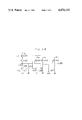
- FIG. 1 is a block diagram of a memory circuit having a known decoder
- FIG. 2 is a circuit diagram of the decoding circuit of the memory circuit shown in FIG. 1;
- FIG. 3A is a block diagram of a memory circuit having a decoder according to the present invention.
- FIG. 3B is a circuit diagram of a driver circuit used in the memory circuit of FIG. 3A for driving the decoder thereof;
- FIG. 4 is a circuit diagram of the decoding circuit of the memory circuit shown in FIG. 3A.
- FIG. 5 is a circuit diagram of a decoding circuit according to another embodiment of the present invention.
- FIG. 3A shows a memory circuit according to the present invention.
- Binary address signals A 0 , A 1 , . . . A n-1 are supplied to address buffers 1.
- These signals A i and A i are supplied to a NOR type decoder 2.
- the output lines or word line W j are connected respectively to rows of memory cells constituting a memory cell array 3. Hence each output line or word-line W j designates the corresponding row of cells when it is enabled.
- the NOR type decoder 2 comprises a plurality of decoding circuits 20 to which the output lines W j are connected, respectively, When all the address signals A i have a logic value "0" and thus designate the 0th address, the output line or word line W 0 is enabled and is turned to a logic value "1". In this case, therefore, the decoding circuit 20 functions as a NOR circuit.
- column C 0 is designated by a column decoder 5 and thus, the content of only the memory cell connected to the word line W 0 and connected to the bit lines D and D for column C 0 is output through a route of the output line 50 of the column decoder 5, the sense amplifier 51 and the data output buffer 52.
- the data input through a data input buffer 53 and a write amplifier 54 is written in, for example, a memory cell connected to the word line W 0 activated by the decoder 2 and connected to a column C 0 designated by the column decoder 5.
- a write-enable buffer 55 controls the data input buffer 53 to form a write-enable condition and also controls the data output buffer circuit 52 to obtain the output data.
- the decoder circuit 2 comprises four blocks 0 to 3, each of which is designated by two address signals A n-1 and A n-2 .
- the address signals A n-1 and A n-2 are supplied to the address buffers 1.
- the address buffer 1 generates two output signals A n-1 and A n-2 and two more output signals A n-1 and A n-2 are obtained by inverting the signals A n-1 and A n-2 .
- These four signals A n-1 , A n-2 , A n-1 and A n-2 are supplied to a two-bit decoder circuit 4.
- the two-bit decoder circuit 4 generates four signals BK 0 , BK 1 , BK 2 and BK 3 and four more signals BK 0 , BK 1 , BK 2 and BK 3 obtained by inverting the signals BK 0 , BK 1 , BK 2 and BK 3 , by using NOR circuits 410 and inverters 411.
- the signals BK 0 and BK 0 are coupled to the decoding circuits 20 of the block 0.
- the signals BK 1 and BK 1 are coupled to the decoding circuits 20 of the block 1, the signals BK 2 and BK 2 to the decoding circuits 20 of the block 2, and the signals BK 3 and BK 3 to the decoding circuits 20 of the block 3.
- FIG. 3B The detailed circuit diagram of the NOR circuit 410 and the inverter 411 in the decoder circuit 4 is shown in FIG. 3B, using MOS transistors.
- the address signals A n-1 and A n-2 are input to the respective gates of the transistor 4010 and 4020.
- the signals A n-1 and A n-2 are at the logic "1"
- either of transistors 4010 and 4020 is turned on.
- the chip select signal CS is at the logic "1”
- a transistor 4030 is turned on, thereby causing current to flow through a load transistor 4040.
- the cross point 4050 becomes the logic "0", thereby turning the transistors 4060 and 4070 off.
- the gate of a transistor 4080 comes up to a high level, i.e., logic "1", and is caused to turn on.
- the block designating signal BK 0 is a low level, i.e. logic "0". Then as a transistor 4100 is turned off, the block designating signal BK 0 is turned to a logic "1".
- both of the address signals A n-1 and A n-2 input to the transistors 4010 and 4020 are at the logic "0"
- the transistors 4060 and 4070 are turned on as they have high level signals at their gates, causing the transistor 4080 to turn off.
- the block designating signal BK 0 becomes the logic "1”.
- the transistor 4100 is turned on, thereby causing the block designating signal BK 0 to have a logic "0".
- the block designating signal BK 0 is output as the output of the NOR circuit when the address input signals A n-2 and A n-1 are input thereto. And the signal BK 0 is the inverted signal of the signal BK 0 .
- FIG. 4 shows each of the decoding circuits 20 used in the memory circuit shown in FIG. 3A.
- the decoding circuit of FIG. 4 is one of the decoding circuits 20 of the block 0 of the memory circuit shown in FIG. 3A.
- the signal BK 0 which designates the block 0 is supplied to the gate of transistor T 1 and the drain of a transistor T 2 . But the output signal BK 0 of the decoder circuit 4 is not supplied to the decoding circuit 20.
- the decoding circuit 20 supplies an output of a logic value "1" through its word line WD only when the block designating signal BK 0 has a logic value "1" and, at the same time, all the address signals A 0 -A n-3 have a logic value "0".
- the decoding circuit 20 is similar to the decoding circuit 20 shown in FIG. 2.
- the decoding circuit 20 supplies an output of a logic value "0" through its word line WD. Accordingly, the decoding circuit 20 functions as a NOR circuit.
- the drain of the transistor T 2 of the decoding circuit 20 is connected to a signal line for supplying the block designating signal BK 0 to the block 0. Therefore, when the word line WD (i.e. output line W 0 in FIG. 3A) is rendered active, the rising of the output signal is inevitably delayed and becomes unstable.
- the word line WD i.e. output line W 0 in FIG. 3A
- FIG. 5 shows another decoding circuit 20 which eliminates the above-mentioned drawback of the decoding circuit 20 shown in FIG. 4.
- this decoding circuit has a transistor 10 having a gate 103 which receives a block designating signal BK 0 having a drain 101 which is connected to a voltage source V CC , a transistor 20 having a drain 201 which is connected to the source 102 of the transistor 10 and the gate 203 and source 202 of which are connected to each other, and a transistor 30 having a drain 301 which is connected to the source 202 of the transistor 20, having a source 302 which is grounded and having a gate 303 which is coupled to receive a signal BK 0 obtained by inverting the block designating signal BK 0 .
- the decoding circuit further comprises a transistor 40 having a gate 403 connected to the source 202 of the transistor 20, having a drain 401 coupled to the voltage source V CC and having a source 402 connected to the word line WD.
- the decoding circuit still further comprises a plurality of transistors 50A to 50B. To gates 50A3 to 50B3 of these transistors 50A to 50B, the address signals A 0 to A n-3 are respectively applied.
- the drains 50A1 to 50B1 of the transistors 50A to 50B are connected commonly to the source 202 of the transistor 20, and the sources 50A2 to 50B2 are connected commonly to the ground.
- the decoding circuit of FIG. 5 is further provided with a transistor 60 whose gate 603 is connected to the drains 50A1 to 50B1 of the n-2 transistors 50A to 50B and whose drain 601 is connected to a gate 703 and source 702 of a load MOS transistor 70, the drain of which is coupled to the voltage source V CC .
- the source 602 of the transistor 60 is grounded.
- Still another transistor 80 is provided, having a gate 803 connected to the drain 601 of the transistor 60, having a drain 801 connected to the word line WD and having a source 802 connected to ground.
- the block 0 of the decoder 2 is comprised of a plurality of decoding circuits 20 which may be the same as the decoding circuits shown in FIG. 5.
- Each of the decoding circuits 20 of block 1 is connected to receive two block designating signals BK 0 and BK 0 .
- the logic values of these signals BK 0 and BK 0 determine whether or not the block 0 is rendered active or selected. Hence, only those of the blocks 0 to 3 which are selected become operative, and the non-selected blocks remain in-operative.
- the block designating signal BK 0 is fed to the gate 103 of the transistor 10 and the reversed block designating signal BK 0 to the gate 303 of the transistor 30.
- the word line WD of the decoding circuit is selected when all the word address signals A 1 -A n-3 are set to a low level (i.e. logical value "0"), and at the same time, both address lines A n-1 and A n-2 have a logic value "0".
- the signal BK 0 is at a high level and the signal BK 0 is at a low level, whereby the 0th address of the block 0, i.e. word line W 0 , is rendered active.
- the transistor is turned on, and the transistor 30 and the transistors 50A-50B receive the address signals and function as NOR circuits.
- no drain current flows in the transistor 10 or 20 and a voltage of V CC appears at a node C1 and thus sets the node C1 to a high level.
- a high-level voltage is applied to the gate 603 of the transistor 60, and current flows to the drain 601 of the transistor 60 through the load MOS transistor 70. Consequently, a high-level voltage is applied to the gate 403 of the transistor 40 and a low-level voltage is applied to the gate 803 of the transistor 80.
- the transistors 40 and 80 are thus turned on and off, respectively.
- the block designating signal BK 0 has a low level and the block designating signal BK 0 has a high level when the block 0 is not selected.
- the word address lines WA are set to either a high level or a low level, the transistor 10 is turned off, and no current flows through the transistor 10.
- the node C1 is set to a low level and the node C2 is set to a high level.
- An output of a logic value "0" is therefore supplied through the word line WD which is now set to a low level. If this is the case, the block 0 consumes no power.
- the memory circuit is so designed that the block designating signal BK 0 is at a low level when a chip selection signal CS is at a high level. Hence, when the block designating signal BK 0 has a low level, the block 0 is placed in a "stand-by” state. That is, the block can be brought into "stand-by” state without using a chip selection signal CS or CS.
- the present invention is characterized in that the most significant binary address signals are used, instead of the chip selection signals as in the prior art, to provide block designating signals for designating a plurality of blocks which comprise a decoder, whereby the current flowing in any block not designated by a block designating signal is reduced substantially to zero.
- the present invention can provide a memory circuit with a decoder which comprises a plurality of blocks and in which substantially no current is supplied to any block when the block is not designated.
- the block designating signals BK 0 and BK 0 are generated from the most significant word address signals A. If the decoder comprises four blocks as shown in FIG. 3A, the block designating signal BK 0 may be a logical sum of the most significant word address WA n-1 and the second most significant word address bit WA n-2 .
Landscapes
- Engineering & Computer Science (AREA)
- Microelectronics & Electronic Packaging (AREA)
- Static Random-Access Memory (AREA)
- Dram (AREA)
Applications Claiming Priority (2)
| Application Number | Priority Date | Filing Date | Title |
|---|---|---|---|
| JP55-187955 | 1980-12-29 | ||
| JP55187955A JPS5857838B2 (ja) | 1980-12-29 | 1980-12-29 | デコ−ド回路 |
Publications (1)
| Publication Number | Publication Date |
|---|---|
| US4470133A true US4470133A (en) | 1984-09-04 |
Family
ID=16215082
Family Applications (1)
| Application Number | Title | Priority Date | Filing Date |
|---|---|---|---|
| US06/331,289 Expired - Fee Related US4470133A (en) | 1980-12-29 | 1981-12-16 | Memory circuit having a decoder |
Country Status (5)
| Country | Link |
|---|---|
| US (1) | US4470133A (fr) |
| EP (1) | EP0055582B1 (fr) |
| JP (1) | JPS5857838B2 (fr) |
| DE (1) | DE3176075D1 (fr) |
| IE (1) | IE53053B1 (fr) |
Cited By (5)
| Publication number | Priority date | Publication date | Assignee | Title |
|---|---|---|---|---|
| US4561070A (en) * | 1983-07-01 | 1985-12-24 | Raytheon Company | Integrated circuit memory |
| US4616345A (en) * | 1982-12-07 | 1986-10-07 | Itt Industries, Inc. | Semiconductor memory |
| US4661724A (en) * | 1985-05-06 | 1987-04-28 | Motorola, Inc. | Row decoder |
| US5815024A (en) * | 1993-06-11 | 1998-09-29 | Altera Corporation | Look-up table using multi-level decode |
| US6037829A (en) * | 1993-06-11 | 2000-03-14 | Altera Corporation | Look-up table using multi-level decode |
Families Citing this family (5)
| Publication number | Priority date | Publication date | Assignee | Title |
|---|---|---|---|---|
| JPS589285A (ja) * | 1981-07-08 | 1983-01-19 | Toshiba Corp | 半導体装置 |
| JPS5933886A (ja) * | 1982-08-20 | 1984-02-23 | Hitachi Ltd | シリコン太陽電池 |
| DE3235662A1 (de) * | 1982-09-27 | 1984-03-29 | Siemens AG, 1000 Berlin und 8000 München | Decoderschaltung fuer auswahlleitungen von halbleiterspeichern |
| JPS59157884A (ja) * | 1983-02-25 | 1984-09-07 | Nec Corp | 半導体メモリ装置 |
| JPS61199297A (ja) * | 1985-02-28 | 1986-09-03 | Toshiba Corp | 半導体記憶装置 |
Citations (5)
| Publication number | Priority date | Publication date | Assignee | Title |
|---|---|---|---|---|
| US3703710A (en) * | 1970-01-05 | 1972-11-21 | Hitachi Ltd | Semiconductor memory |
| US3750116A (en) * | 1972-06-30 | 1973-07-31 | Ibm | Half good chip with low power dissipation |
| US3803554A (en) * | 1971-05-04 | 1974-04-09 | Ibm | Apparatus for addressing an electronic data storage |
| US3815106A (en) * | 1972-05-11 | 1974-06-04 | S Wiedmann | Flip-flop memory cell arrangement |
| US4387449A (en) * | 1979-11-08 | 1983-06-07 | Nippon Electric Co., Ltd. | Programmable memory device having reduced power consumption upon unselection |
-
1980
- 1980-12-29 JP JP55187955A patent/JPS5857838B2/ja not_active Expired
-
1981
- 1981-12-16 US US06/331,289 patent/US4470133A/en not_active Expired - Fee Related
- 1981-12-22 EP EP81306024A patent/EP0055582B1/fr not_active Expired
- 1981-12-22 DE DE8181306024T patent/DE3176075D1/de not_active Expired
- 1981-12-23 IE IE3067/81A patent/IE53053B1/en unknown
Patent Citations (5)
| Publication number | Priority date | Publication date | Assignee | Title |
|---|---|---|---|---|
| US3703710A (en) * | 1970-01-05 | 1972-11-21 | Hitachi Ltd | Semiconductor memory |
| US3803554A (en) * | 1971-05-04 | 1974-04-09 | Ibm | Apparatus for addressing an electronic data storage |
| US3815106A (en) * | 1972-05-11 | 1974-06-04 | S Wiedmann | Flip-flop memory cell arrangement |
| US3750116A (en) * | 1972-06-30 | 1973-07-31 | Ibm | Half good chip with low power dissipation |
| US4387449A (en) * | 1979-11-08 | 1983-06-07 | Nippon Electric Co., Ltd. | Programmable memory device having reduced power consumption upon unselection |
Cited By (6)
| Publication number | Priority date | Publication date | Assignee | Title |
|---|---|---|---|---|
| US4616345A (en) * | 1982-12-07 | 1986-10-07 | Itt Industries, Inc. | Semiconductor memory |
| US4561070A (en) * | 1983-07-01 | 1985-12-24 | Raytheon Company | Integrated circuit memory |
| US4661724A (en) * | 1985-05-06 | 1987-04-28 | Motorola, Inc. | Row decoder |
| US5815024A (en) * | 1993-06-11 | 1998-09-29 | Altera Corporation | Look-up table using multi-level decode |
| US6037829A (en) * | 1993-06-11 | 2000-03-14 | Altera Corporation | Look-up table using multi-level decode |
| US6351152B1 (en) * | 1993-06-11 | 2002-02-26 | Altera Corporation | Look-up table using multi-level decode |
Also Published As
| Publication number | Publication date |
|---|---|
| IE53053B1 (en) | 1988-05-25 |
| IE813067L (en) | 1982-06-29 |
| JPS57113481A (en) | 1982-07-14 |
| JPS5857838B2 (ja) | 1983-12-22 |
| EP0055582A2 (fr) | 1982-07-07 |
| EP0055582A3 (en) | 1984-04-11 |
| DE3176075D1 (en) | 1987-05-07 |
| EP0055582B1 (fr) | 1987-04-01 |
Similar Documents
| Publication | Publication Date | Title |
|---|---|---|
| US4389705A (en) | Semiconductor memory circuit with depletion data transfer transistor | |
| US5969995A (en) | Static semiconductor memory device having active mode and sleep mode | |
| US5301144A (en) | Semiconductor memory device having a decoding circuit for reducing electric field stress applied to memory cells | |
| USRE36655E (en) | Semiconductor memory device and method for reading and writing data therein | |
| US4631707A (en) | Memory circuit with power supply voltage detection means | |
| US5708599A (en) | Semiconductor memory device capable of reducing power consumption | |
| US4374430A (en) | Semiconductor PROM device | |
| US4393472A (en) | Semiconductor memory circuit | |
| US5396124A (en) | Circuit redundancy having a variable impedance circuit | |
| US4259731A (en) | Quiet row selection circuitry | |
| EP0055582B1 (fr) | Circuit de mémoire à décodeur | |
| KR970000331B1 (ko) | 반도체 기억장치 | |
| US5668485A (en) | Row decoder with level translator | |
| US5517461A (en) | Semiconductor storage device having latch circuitry coupled to data lines for eliminating through-current in sense amplifier | |
| KR970051351A (ko) | 다중값 정보를 기록할 수 있는 비휘발성 반도체 메모리 | |
| US4982365A (en) | Semiconductor memory device with a potential level-setting circuit | |
| JPH07211077A (ja) | 半導体記憶装置 | |
| EP0259862B1 (fr) | Mémoire à semi-conducteurs avec fonction d'écriture | |
| EP0136229A2 (fr) | Amplificateur de lecture | |
| US4563598A (en) | Low power consuming decoder circuit for a semiconductor memory device | |
| EP0271283B1 (fr) | Dispositif de mémoire à semi-conducteurs ayant une opération de hausse de tension pour lignes de but | |
| KR910014938A (ko) | 향상된 di/dt 제어가 가능한 집적회로 메모리 | |
| US4986666A (en) | Semiconductor memory device | |
| JPH0368479B2 (fr) | ||
| JPH0766675B2 (ja) | プログラマブルrom |
Legal Events
| Date | Code | Title | Description |
|---|---|---|---|
| AS | Assignment |
Owner name: FUJITSU LIMITED, 1015, KAMIKODANAKA, NAKAHARA-KU, Free format text: ASSIGNMENT OF ASSIGNORS INTEREST.;ASSIGNOR:TANIMOTO, KAZUO;REEL/FRAME:003957/0680 Effective date: 19811209 |
|
| CC | Certificate of correction | ||
| FPAY | Fee payment |
Year of fee payment: 4 |
|
| REMI | Maintenance fee reminder mailed | ||
| LAPS | Lapse for failure to pay maintenance fees | ||
| FP | Lapsed due to failure to pay maintenance fee |
Effective date: 19920906 |
|
| STCH | Information on status: patent discontinuation |
Free format text: PATENT EXPIRED DUE TO NONPAYMENT OF MAINTENANCE FEES UNDER 37 CFR 1.362 |