US4683384A - Integrated circuit having input and output drivers cascaded between I/O pads and internal circuitry - Google Patents
Integrated circuit having input and output drivers cascaded between I/O pads and internal circuitry Download PDFInfo
- Publication number
- US4683384A US4683384A US06/895,216 US89521686A US4683384A US 4683384 A US4683384 A US 4683384A US 89521686 A US89521686 A US 89521686A US 4683384 A US4683384 A US 4683384A
- Authority
- US
- United States
- Prior art keywords
- input
- output
- circuit
- external connection
- signal transmission
- Prior art date
- Legal status (The legal status is an assumption and is not a legal conclusion. Google has not performed a legal analysis and makes no representation as to the accuracy of the status listed.)
- Expired - Fee Related
Links
Images




Classifications
-
- H—ELECTRICITY
- H03—ELECTRONIC CIRCUITRY
- H03K—PULSE TECHNIQUE
- H03K19/00—Logic circuits, i.e. having at least two inputs acting on one output; Inverting circuits
- H03K19/02—Logic circuits, i.e. having at least two inputs acting on one output; Inverting circuits using specified components
- H03K19/173—Logic circuits, i.e. having at least two inputs acting on one output; Inverting circuits using specified components using elementary logic circuits as components
- H03K19/177—Logic circuits, i.e. having at least two inputs acting on one output; Inverting circuits using specified components using elementary logic circuits as components arranged in matrix form
- H03K19/17736—Structural details of routing resources
- H03K19/17744—Structural details of routing resources for input/output signals
-
- H—ELECTRICITY
- H03—ELECTRONIC CIRCUITRY
- H03K—PULSE TECHNIQUE
- H03K19/00—Logic circuits, i.e. having at least two inputs acting on one output; Inverting circuits
- H03K19/0175—Coupling arrangements; Interface arrangements
- H03K19/017509—Interface arrangements
- H03K19/017518—Interface arrangements using a combination of bipolar and field effect transistors [BIFET]
-
- H—ELECTRICITY
- H03—ELECTRONIC CIRCUITRY
- H03K—PULSE TECHNIQUE
- H03K19/00—Logic circuits, i.e. having at least two inputs acting on one output; Inverting circuits
- H03K19/02—Logic circuits, i.e. having at least two inputs acting on one output; Inverting circuits using specified components
- H03K19/173—Logic circuits, i.e. having at least two inputs acting on one output; Inverting circuits using specified components using elementary logic circuits as components
- H03K19/177—Logic circuits, i.e. having at least two inputs acting on one output; Inverting circuits using specified components using elementary logic circuits as components arranged in matrix form
- H03K19/17704—Logic circuits, i.e. having at least two inputs acting on one output; Inverting circuits using specified components using elementary logic circuits as components arranged in matrix form the logic functions being realised by the interconnection of rows and columns
-
- H—ELECTRICITY
- H03—ELECTRONIC CIRCUITRY
- H03K—PULSE TECHNIQUE
- H03K19/00—Logic circuits, i.e. having at least two inputs acting on one output; Inverting circuits
- H03K19/02—Logic circuits, i.e. having at least two inputs acting on one output; Inverting circuits using specified components
- H03K19/173—Logic circuits, i.e. having at least two inputs acting on one output; Inverting circuits using specified components using elementary logic circuits as components
- H03K19/177—Logic circuits, i.e. having at least two inputs acting on one output; Inverting circuits using specified components using elementary logic circuits as components arranged in matrix form
- H03K19/1778—Structural details for adapting physical parameters
Definitions
- This invention relates generally to an integrated circuit. More particularly, the present invention relates to technique which can be applied effectively to an integrated circuit having regions in which a plurality each of input and output circuits can be formed in such a manner as to form pairs that correspond to a plurality of external connection pads, respectively, such as gate arrays.
- Integrated circuits (which will also be called “ICs” hereafter) can be broadly classified into ICs having high versatility, such as standard logic semiconductor integrated circuits, and custom ICs, such as gate arrays, that are produced in accordance with customers' requirements. Being mass-produced, versatile ICs are economical but are not free from the problem that a large number of ICs are necessary in order to form circuits that are required by customers. The custom ICs are produced in order to solve this problem. Various contrivances are made to the custom ICs in order to satisfy customers' requirements. An example of such contrivances can be seen in ICs for gate arrays.
- a large number of buffer portions are formed around an internal circuit which includes a large number of basic cells.
- the internal circuit includes a large number of basic cells in order to easily form a logic circuit required by a customer, and the desired logic circuit can be constituted within a short period by connecting these basic cells by aluminum wirings, whenever necessary.
- the buffer portions have an input circuit region and an output circuit region so that the input and output circuits can form pairs which correspond to a plurality of external connection pads, and that the arrangement of the input-output pins can be obtained easily as stipulated by the customer.
- the corresponding external connection pads are input pins, only the input circuit region is used with the output circuit region being not used.
- the corresponding external connection pads are output pins, on the contrary, only the output circuit region is used while the input circuit region is not used.
- the utilization ratio of an internal circuit portion has become extremely high as the scale of systems is ever-increasing. However, only a predetermined number of basic cells, which are contained in the internal circuit, are disposed on one main plane of a substrate. On the other hand, as to the buffer portion, the utilization ratio is low and many useless regions are contained as described above.
- the present invention contemplates to improve the substrate utilization ratio of custom ICs such as gate arrays.
- a plurality of each of input and output circuits are disposed on the main surface of a substrate in such a manner as to form pairs that correspond to a plurality of external connection pads, respectively, and are used selectively, and the signal transmission function of the non-selected input or output circuits (which are not used in the prior art circuits) is used as part of the functions of an internal circuit.
- a signal transmission path of an input circuit formed so as to correspond to an external connection pad to which an external input signal is applied, and at least part of a signal transmission path of an output circuit formed so as to correspond to the external connection pad are connected in series between the external connection pad and an input terminal of the internal circuit in order to use the signal transmission function of the output circuit as the function of the internal circuit.
- At an output portion on the other hand, at least part of the signal transmission path of an input circuit formed so as to correspond to an external connection pad for delivering an output signal to the outside and a signal transmission path of an output circuit formed so as to correspond to the external connection pad are connected in series between the output terminal of the internal circuit and the external connection pad in order to use the signal transmission function of the input circuit as the function of the internal circuit.
- the non-selected input and output circuits that are not used in the prior art, are positively used in the present invention to eliminate the useless space on the substrate and to improve the substrate utilization ratio. Furthermore, even when the utilization ratio of the internal circuit is high, at least part of the signal transmission function of the input and output circuits can easily replace the function of the internal circuit.
- the two methods described above can be applied to all the input circuits and output circuits that are formed so as to correspond to the external connection pads, but can of course be applied to at least one of these external connection pads. In such a case, an ordinary method can be applied to those portions to which the present invention is not applied.
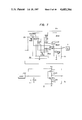
- FIG. 1 is a conceptual view showing one embodiment of the present invention
- FIG. 2 is a block diagram showing a gate array to which the present invention is applied;
- FIG. 3 is a plan view of a device layout showing the internal state of a gate array to which the present invention is applied;
- FIG. 4 is a circuit diagram showing an example of an input circuit
- FIG. 5 is a circuit diagram showing an example of an output circuit
- FIG. 6 is a definite circuit diagram showing the circuit portions near an external connection pad portion for input to which the present invention is applied;
- FIG. 7 is a definite circuit diagram showing the circuit portions near an external connection pad portion for output to which the present invention is applied;
- FIG. 8 is a plan view of device layout of a gate array to which the present invention is applied.
- FIGS. 9 to 11 show the construction of basic cells, respectively.
- FIGS. 12 and 13 show an example of the circuit constituted by use of the basic cells.
- FIG. 14 shows an example of the content of a buffer portion.
- FIG. 1 shows an example of the principal portions of an integrated circuit (hereinafter called “IC” or “semiconductor integrated circuit device”).
- IC integrated circuit
- This drawing shows the portions close to an I/O (input/output) buffer portion 2 of a semiconductor integrated circuit device in which a gate array is formed.
- the buffer portion 2 is disposed between an internal circuit 200 and an external connection pad 3.
- a region 2a for an input buffer circuit (111) as an input circuit and a region 2b for an output buffer circuit 121 as an output circuit are formed as a pair on one main surface of a substrate of the buffer portion 2 which is disposed in such a manner as to correspond to the external connection pad 3.
- Circuit elements (such as diodes, transistors, resistors, etc.) for constituting the input buffer circuit (111) are formed in the region 2a, while circuit elements for constituting the output buffer circuit 121 are formed in the region 2b.
- the buffer portion 2 shown in FIG. 1 is used as an output buffer portion. Therefore, the output buffer portion 121 is formed in the region 2b, while all the circuit elements of the input buffer circuit (111) are not connected in the region 2a. Instead, a circuit 111' formed by connecting part of the circuit elements of the input buffer circuit (111) is formed in the region 2a where the input buffer circuit (111) is to be formed. In other words, the circuit 111' formed in the region 2a is utilized as a substitute for basic cells in the internal circuit 200.
- At least a part of a signal transmission path between the input and output of the input circuit, which is formed in such a manner as to correspond to the external connection pad 3 (the signal transmission path of the circuit 111'), and a signal transmission path between the input and output of the output circuit 121 formed in such a manner as to correspond to the pad 3 are connected in series between the output terminal of the internal circuit 200 and the pad 3, so that the output signal of the output circuit 121 is responsive to the output signal from the output terminal of the internal circuit 200 in the signal transmission relation that is determined by the signal transmission function of the input circuit (the circuit 111') and the signal transmission function of the output circuit 121, and the output signal of the output circuit 121 is delivered from the external connection pad 3 outside the integrated circuit IC.
- the signal transmission function of the circuit 111' formed by use of a part of the input circuit is utilized as a substitute for the logical function of the internal circuit 200.
- the circuit elements for constituting the input buffer circuit (or the output buffer circuit) inside the buffer portion 2 is utilized in place of the basic cells inside the internal circuit 200, it becomes possible to more effectively utilize the circuit elements inside the buffer portion 2, to increase the number of basic cells that can be utilized in practice, and to improve the function of a gate array having the same scale.
- FIG. 2 shows the outline of the gate array.
- an input buffer portion 110 and output buffer portion 120 are formed together with an internal circuit 200 in a semiconductor integrated circuit device IC in which the gate array is constituted.
- the input and output buffer portions 110 and 120 are interposed between external connection pads 3 and the internal circuit 200, respectively, and function as buffers involving level conversion.
- V ith represents an input threshold value
- V IH is an input logic level at the time of a high (H) level
- V OH is an output logic level at the time of the high (H) level
- V IL is an input logic level at the time of a low (L) level
- V OL is an output logic level at the time of the low (L) level.
- Symbols inl ⁇ ink represent logic inputs to the outside and outl ⁇ outm represent logic outputs to the outside.
- the logic input/output to the outside is at a TTL level (with the high level of being at least 2.0 V and the low level being up to 0.8 V) while the logic level inside IC is at a CMOS level (with the high level being at least 4.4 V and the low level being up to 0.6 V).
- FIG. 3 shows the outline of the circuits inside the semiconductor integrated circuit device IC of FIG. 2.
- a large number of logic function units (micro-cells) 201 ⁇ 20n and wirings (dotted lines) for mutually connecting these units are formed inside the internal circuit 200 in accordance with a customer's requirement.
- a large number of input buffer circuits 111 are formed in the input buffer portion 110 while a large number of output buffer circuits 121 are formed in the output buffer portion 120 in a corresponding manner.
- a plurality of input buffer circuits 111 and a plurality of output buffer circuits 121 are disposed on the main surface of the substrate 10 around the internal circuit 200 in such a manner as to form pairs with respect to a plurality of external connection pads 3.
- the portions to which the present invention are applied are those represented by symbols A and B in the drawing.
- the input circuit 111 and the output circuit 121 are interposed in series between the external connection pad 3 and the unit 202 of the internal circuit 200.
- the input circuit 111' that has been described with reference to FIG. 1 and the output circuit 121 are interposed in series between the output terminal of the unit 20n of the internal circuit 200 and the external connection pad 3. Since the signal transmission path is constituted in this manner, a logic function such as that performed by the internal circuit 200 replaces the normal output signal transmission function of the output circuit 121 in the A portion (and the normal input signal transmission function of the input circuit 111' in the B portion).
- the input circuit 111 is shown disposed between the external connection pad (first pad) 3 and the input terminal of the unit 201 of the internal circuit in the portion represented by symbol C.
- the input signal is transferred to the unit 201 of the internal circuit 200 without passing through the signal transmission path of the output circuit 121 formed in such a manner as to correspond to ths first pad 3.
- the output circuit 121 is shown disposed between the output terminal of the unit 203 of the internal circuit and the external connection pad (second pad) 3, and the output signal of the unit 203 of the internal circuit 200 is transferred to this second pad 3 without passing through the signal transmission path of the input circuit 111 formed in such a manner as to correspond to the second pad 3.
- the output circuit 121 of the A portion and the input circuit 111' of the B portion will be modified to differ somewhat from the output circuit 121 of the D portion and the input circuit 111 of the C portion. However, at least part of their signal transmission path is utilized which would otherwise be wasted.
- reference numeral 11 represents a lead and 12 represents a wire.
- An input signal to IC from outside IC and an output signal from IC to outside IC are applied and taken out, respectively, through the lead 11 and the wire 12.
- FIG. 4 shows an example of the circuit corresponding to the C portion shown in FIG. 3.
- the input circuit 111 is comprised of a P-channel MOS field effect transistor M 11 , N-channel MOS field effect transistors M 12 , M 13 , NPN type bipolar transistors Q 11 , Q 12 , a PNP type bipolar transistor Q 13 , diodes D 11 , D 12 and resistors R 11 , R 12 , R 13 .
- the PNP transistor Q 13 as the input stage circuit receives a logic input of the TTL level applied to the external connection pad 3.
- the PNP transistor Q 13 When the level of the logic input signal is at the low level (L: up to 0.8 V), the PNP transistor Q 13 becomes conductive and shifts down the level of a CMOS inverter as a next stage circuit comprised of the MOS field effect transistors M 11 , M 12 to the low level, so that the bipolar transistors Q 11 and Q 12 of the totempole output stage are turned on and off, respectively, and the output OUT is shifted up to the high (H) level.
- the logic input signal is at the high level (H: at least 2.0 V)
- the bipolar transistor Q 12 becomes conductive while Q 11 becomes non-conductive so that the output OUT falls to the low level.
- the signal transmission function of this input circuit 111 is to perform the logic function of an inverter.
- a diode D 11 as an input protection circuit is added to the input buffer circuit 111 shown in FIG. 4. Since the PNP bipolar transistor Q 13 whose dielectric breakdown strength is greater than that of the MOS transistors M 11 , M 12 is used as the input stage circuit, the dielectric breakdown strength with respect to static electricity that might be applied from the pad 3 can be improved.
- FIG. 5 shows an example of the circuit of the output circuit 121 of the D portion shown in FIG. 3.
- This output buffer circuit 121 consists of MOS field effect transistors M 21 ⁇ M 30 , bipolar transistors Q 21 , Q 22 , diodes D 21 ⁇ D 23 and resistors R 21 , R 22 .
- This output buffer circuit 121 is a tri-state type inverter, and symbol EN represents a control signal which selects its output state.
- the MOS field effect transistors M 24 and M 29 constitute a CMOS inverter and drives the base electrode of the bipolar transistor Q 21 by a signal having the opposite phase to that of the input signal.
- the source-follower transistors M 27 and M 29 drive the base electrode of the bipolar transistor Q 22 by a signal having the same phase as that of the input signal.
- the source-follower transistor M 27 is disposed in order to drive the base electrode of Q 22 at a high level (near a power source voltage V cc ).
- the source-follower transistor M 29 supplies the charge of the output OUT to the base electrode of the bipolar transistor Q 22 through the diode D 23 and the source-drain path of the MOS field effect transistor M 31 .
- a current which is the product of the charge supplied to the base electrode by the current amplification factor flows through the collector-emitter path of the bipolar transistor Q 22 and discharges at a high speed the charge of the output OUT.
- both the MOS field effect transistors M 28 and M 30 become conductive, and since the base electrodes of the bipolar transistors Q 21 and Q 22 fall to the low (L) level, the output OUT of the output circuit 121 is brought into the floating state irrespective of the logic level of the input signal from the input in of the output circuit.
- the control signal EN is at the low (L) level, both the transistors M 28 and M 30 are non-conductive and the CMOS inverter consisting of the field effect transistors M 24 and M 29 becomes operative.
- the base electrode of the bipolar transistor Q 22 When the logic level of the input signal is at the high level, the base electrode of the bipolar transistor Q 22 is shifted up to the high level, whereby Q 22 is conductive with Q 21 being non-conductive, and the output OUT of the output circuit 121 falls down to the low level.
- the base electrode of the bipolar transistor Q 21 When the logic level of the input signal is at the low level, the base electrode of the bipolar transistor Q 21 is shifted up to the high level, whereby Q 21 becomes conductive with Q 22 being non-conductive and the output OUT of the output circuit 121 is shifted up to the high level.
- FIG. 6 shows an example of the circuit of the A portion shown in FIG. 3.
- the circuit shown in FIG. 6 consists of the combination of the input buffer circuit 111 and the output buffer circuit 121 shown in FIGS. 4 and 5, respectively.
- the terminal, to which the control signal EN is applied in FIG. 5 is grounded (to a ground potential GND). Therefore, the output circuit 121 shown in FIG. 6 is an ordinary inverter which will operate at the CMOS levels shown in FIG. 2 rather than converting the CMOS levels to TTL levels.
- the external input signal applied to the external connection pad 3 passes through the signal transmission path between the input and output of the input buffer circuit 111, then through the signal transmission path of the input and output of the output circuit 121 and is transmitted to the internal circuit 200.
- the output signal of the output buffer circuit 121 responds to the external input signal in the signal transmission relation that is determined by the signal transmission function of the input buffer circuit 111 (the inverter) and the signal transmission function of the output circuit 121 (the inverter), and is applied to the internal circuit 200.
- the external input signal is transmitted in the same phase to the internal circuit 200 and at the CMOS level.
- FIG. 7 shows an example of the circuit of the B portion shown in FIGS. 1 and 3.
- the diagram shows an example wherein the output circuit 121 shown in FIG. 5 and the inverter circuit 111' using part of the signal transmission path of the input buffer circuit 111 shown in FIG. 4 are connected.
- the output signal of the internal circuit 200 passes through part of the signal transmission path of the input buffer circuit 111 (the signal transmission path of the inverter circuit 111') and is then transmitted to the external connection pad 3 through the signal transmission path of the output buffer circuit 121, and delivered outside the integrated circuit.
- the inverter circuit 111' shown in this drawing consists of the MOS field effect transistors M 11 , the bipolar transistor Q 11 , Q 12 and the resistors R 12 , R 13 inside the input buffer circuit 111 shown in FIG. 4.
- the characterizing feature of this circuit is that the PNP transistor Q 13 as the input stage circuit of the input buffer circuit 111 is deliberately not connected to at least part of the signal transmission path between the input and output of the input circuit.
- the logic input signal supplied to the input terminal in of the input buffer circuit 111 shown in FIG. 4 is a TTL level signal whose high level input voltage V iH is at least 2.0 V and whose low level input voltage V iL is up to 0.8 V. Therefore, the input threshold voltage V ith of the input buffer circuit 111 is set to the range of from 1.3 to 1.5 V between 0.8 V 2.0 V.
- the input signal applied to the input of the inverter circuit 111' shown in FIG. 7 is at the CMOS level whose high level input voltage V IH is at least 4.4 V and whose low level input voltage V IL is up to 0.6 V. Therefore, the input logic threshold voltage V ith of the inverter circuit 111' may be set to a voltage ranging from about 2.0 to about 3.0 V between these voltages 4.4 V and 0.6 V. In other words, it is necessary that the PNP transistor Q 13 be positively disconnected when the CMOS level input signal supplied from the internal circuit 200 is received without changing the input logic threshold voltage of the CMOS inverter shown in FIG. 4. For the reason described above, the inverter circuit 111' shown in FIG. 7 which corresponds at least to part of the signal transmission path of the input buffer circuit 111 shown in FIG. 4 does not use the PNP transistor Q 13 .
- the ratio W/L between the channel width W and the channel length L of each MOS field effect transistors M 11 , M 12 , M 13 is set to 30/2, 25/2, 32/2, respectively. Therefore, the MOS field effect transistors to be used for the inverter circuit 111' in FIG. 7 may be M 11 and M 13 instead of M 11 and M 12 . In this case, the ratio W/L of the MOS field effect transistor M 11 is approximate to that of the MOS field effect transistor M 13 , so that the input logic threshold voltage can be set easily.
- the inverter circuit 111' shown in FIG. 7 uses the bipolar transistors Q 11 and Q 12 of the totempole type output stage of the input buffer circuit 111.
- the output stage circuit of the bipolar transistors Q 11 and Q 12 is not always necessary. In other words, it is of course possible to use the inverter circuit comprised only of M 11 and M 12 or M 11 and M 13 .
- the present invention can be used effectively and advantageously for the following cases.
- Automatic wiring technique using a computer is used for wiring a plurality of basic cells 1 inside the internal circuit 200 (e.g. see FIG. 8).
- the utilization ratio of the basic cells inside the internal circuit 200 becomes high, however, the automatic wiring technique cannot sometimes wire the basic cells with one another (i.e., non-wiring occurs). This phenomenon becomes significant particularly when the utilization ratio of the basic cells is as high as 95%, and depends upon the program content of the program of the automatic wiring technique.
- the output circuit 121 corresponding to the external connection pad of the input portion and the input circuit 111' corresponding to the external connection pad of the output portion are used to obtain the function of the internal circuit in accordance with the present invention, however, the utilization ratio of the basic cells within the internal circuit 200 drops also even when the automatic wiring technique is used. Incidentally, about two hours' time is necessary for connecting one wiring layer, and the drop of the non-wiring ratio contributes greatly to the reduction of the design time.
- FIG. 8 shows the layout structure of the semiconductor integrated circuit device IC described above.
- reference numeral 1 represents each basic cell. Circuit elements necessary for constituting a basic logic circuit, that is, part or the whole of the circuit elements necessary for constituting the basic logic circuit, are formed in this basic cell 1. A great number of basic cells 1 having the same pattern are arranged. Reference numeral 4 represents each wiring region necessary for communicating the basic cells 1 with one another.
- the logic circuit units (macro-cells) 201 ⁇ 20n shown in FIG. 3 are constituted by use of one or a plurality of basic cells 1.
- Reference numeral 2 represents each I/O buffer portion. Either one of the input buffer circuit 111 and the output buffer circuit 121 is selectively formed in the buffer portion 2. A great number of buffer portions 2 are arranged around the internal circuit portion 200. The internal circuit 200 is disposed in order to receive the output signals of a plurality of input circuits and to generate the output signals for driving the inputs of a plurality of output circuits.
- Reference numeral 3 represents each external connection terminal pad 3.
- a great number of terminal pads 3 are arranged outside the buffer portion 2 around the four sides of a rectangular substrate, and are used as the input terminals or the output terminals in accordance with the kind of the circuits formed in the buffer portions 2 at the corresponding positions.
- terminal pads 3 that are used as the input and output terminals
- terminal pads 3a, 3b that are used as a power terminal and a ground terminal, respectively, are also provided.
- FIGS. 9, 10 and 11 show the content of the basic cell 1 described above.
- circuit elements necessary for constituting the basic logic circuit that is, part or the whole of the circuit elements necessary for constituting the basic logic circuit, are formed inside the basic cell 1.
- P-channel MOSFETs MOS field effect transistors
- M 1 , M 2 , M 3 , N-channel MOSFETS M 4 , M 5 , M 6 , resistors R 1 and R 2 and bipolar transistors Q 1 and Q 2 are formed as shown in FIG. 9.
- FIG. 10 shows the layout state of the basic cell 1.
- reference numeral 11 represents a P + -type diffusion layer forming the source-drain region of the P-channel MOSFETs M 1 , M 2 , M 3 and 12 represents an N + -type diffusion layer forming the source-drain region of the N-channel MOSFETs M 4 , M 5 , M 6 .
- Reference numeral 13 represents an n - -type epitaxial layer portion in which the NPN bipolar transistors Q 1 , Q 2 are to be formed, and 14 represents a diffusion layer for current collection of a collector (C) electrode.
- Reference numeral 15 represents a base (B) diffusion layer
- 16 is an emitter (E) diffusion layer
- 17 is a p-type diffusion layer for forming the resistors R 1 , R 2 .
- Reference numerals 18a, 18b and 18c represent electrode portions which are made of polycrystalline silicon or the like and serve as the gate electrodes of MOSFETs M 1 ⁇ M 6 and as cell terminal portions in1a, in1b, in2a, in2b, in3a, in3b.
- the cell terminal portions in1a, in1b, in2a and in2b are taken outside the basic cell 1, but the terminals in3a and in3b are placed inside the basic cell 1 as hidden terminal portions. They are used for wiring adjacent basic cells with one another, and the like.
- FIG. 11 illustrates the basic cell 1 described above as one block, and its explanation is omitted.
- FIGS. 12 and 13 show an example of circuits constituted by the basic cells 1 described above.
- FIG. 12 shows a definite circuit diagram of the circuit expressed by logic symbols in FIG. 13.
- its pre-stage side consists of MOSFETs M 1 ⁇ M 6 that are connected with one another in a complementary arrangement, while its output stage consists of the bipolar transistors Q 1 and Q 2 .
- This circuit arrangement can accomplish lower power consumption and higher speed operation by higher driving force.
- the logic symbol whose output side is colored black is hereby assumed to represent a logic circuit whose output stage consists of bipolar transistors.
- FIG. 14 shows in further detail the content of the buffer portion 2 described above prior to wiring connections being made. As shown in this diagram, a pair constituted of a region 2a for the input buffer circuit and a region 2b for the output buffer circuit is formed inside the buffer portion 2.
- the present invention connects in series the signal transmission path between the input and output of the input circuit corresponding to one of a plurality of external connection pads and at least a part of the signal transmission path between the input and output of the output circuit between one external connection pad described above and one of the input terminals of the internal circuit. Therefore, the signal transmission function of the output circuit can be utilized as part of the functions of the internal circuit. As a result, the utilization ratio of the substrate having formed thereon the integrated circuit can be improved, and hence the circuit function of the integrated circuit can be improved as a whole.
- At least part of the signal transmission path of the input circuit and the signal transmission path of the output circuit which is disposed in such a manner as to form a pair together with the input circuit and to correspond to the external connection pad, are connected in series between one of the output terminals of the internal circuit and the external connection pad.
- the signal transmission function of the input circuit can be utilized as part of the functions of the internal circuit, so that the utilization ratio of the substrate having formed thereon the integrated circuit can be improved, and the circuit function of the integrated circuit can as a whole be improved.
- the signal transmission function of the input and output circuits may be a linear function instead of a logic function.
- the logic function of the circuit shown in FIG. 6 is not particularly limited to being an inverter.
- the particular elements and circuits shown in the buffers 2 could be changed to allow for other functions while still falling within the scope of this invention in making use of normally unused portions of input or output areas.
- FIG. 7 although a two-FET arrangement of M 11 and M 12 is shown, the three transistors M 11 , M 12 and M 13 could be used together to improve characteristics of the CMOS circuit.
Landscapes
- Physics & Mathematics (AREA)
- Mathematical Physics (AREA)
- Engineering & Computer Science (AREA)
- Computer Hardware Design (AREA)
- Computing Systems (AREA)
- General Engineering & Computer Science (AREA)
- Computer Networks & Wireless Communication (AREA)
- Logic Circuits (AREA)
- Design And Manufacture Of Integrated Circuits (AREA)
Applications Claiming Priority (2)
| Application Number | Priority Date | Filing Date | Title |
|---|---|---|---|
| JP60-174133 | 1985-08-09 | ||
| JP60174133A JPS6235716A (ja) | 1985-08-09 | 1985-08-09 | 半導体集積回路装置 |
Publications (1)
| Publication Number | Publication Date |
|---|---|
| US4683384A true US4683384A (en) | 1987-07-28 |
Family
ID=15973235
Family Applications (1)
| Application Number | Title | Priority Date | Filing Date |
|---|---|---|---|
| US06/895,216 Expired - Fee Related US4683384A (en) | 1985-08-09 | 1986-08-11 | Integrated circuit having input and output drivers cascaded between I/O pads and internal circuitry |
Country Status (2)
| Country | Link |
|---|---|
| US (1) | US4683384A (ja) |
| JP (1) | JPS6235716A (ja) |
Cited By (16)
| Publication number | Priority date | Publication date | Assignee | Title |
|---|---|---|---|---|
| US4761567A (en) * | 1987-05-20 | 1988-08-02 | Advanced Micro Devices, Inc. | Clock scheme for VLSI systems |
| US4839537A (en) * | 1986-11-29 | 1989-06-13 | Kabushiki Kaisha Toshiba | BicMO logic circuit |
| US5017813A (en) * | 1990-05-11 | 1991-05-21 | Actel Corporation | Input/output module with latches |
| US5097150A (en) * | 1989-05-19 | 1992-03-17 | Fujitsu Limited | Bi-cmos logic circuit |
| US5194932A (en) * | 1990-05-30 | 1993-03-16 | Nec Corporation | Semiconductor integrated circuit device |
| US5198986A (en) * | 1989-12-22 | 1993-03-30 | Mitsubishi Denki Kabushiki Kaisha | Crosstalk verification device |
| US5208764A (en) * | 1990-10-29 | 1993-05-04 | Sun Microsystems, Inc. | Method for optimizing automatic place and route layout for full scan circuits |
| US5231589A (en) * | 1989-12-11 | 1993-07-27 | Hitachi, Ltd. | Input/output pin assignment method |
| US5296755A (en) * | 1990-11-29 | 1994-03-22 | Hitachi, Ltd. | High speed BI CMOS logic circuit and a semiconductor integrated circuit device using same |
| US5625567A (en) * | 1993-11-12 | 1997-04-29 | Viewlogic Systems, Inc. | Electronic circuit design system and method with programmable addition and manipulation of logic elements surrounding terminals |
| US5694328A (en) * | 1992-08-06 | 1997-12-02 | Matsushita Electronics Corporation | Method for designing a large scale integrated (LSI) layout |
| US5995740A (en) * | 1996-12-23 | 1999-11-30 | Lsi Logic Corporation | Method for capturing ASIC I/O pin data for tester compatibility analysis |
| US20020143510A1 (en) * | 1994-09-01 | 2002-10-03 | Peters Michael J. | Integrated circuit I/O pad cell modeling |
| US6684378B2 (en) * | 1998-04-23 | 2004-01-27 | Matsushita Electric Industrial Co., Ltd. | Method for designing power supply circuit and semiconductor chip |
| US20050182828A1 (en) * | 1999-04-21 | 2005-08-18 | Interactual Technologies, Inc. | Platform specific execution |
| US20250030422A1 (en) * | 2023-07-18 | 2025-01-23 | Raytheon Company | Compact integrated circuit input with level-shifting to support range of i/o voltages |
Families Citing this family (1)
| Publication number | Priority date | Publication date | Assignee | Title |
|---|---|---|---|---|
| FR2653952A1 (fr) * | 1989-10-31 | 1991-05-03 | Thomson Composants Microondes | Circuit integre logique prediffuse comportant au moins un amplificateur. |
Citations (7)
| Publication number | Priority date | Publication date | Assignee | Title |
|---|---|---|---|---|
| US4350906A (en) * | 1978-06-23 | 1982-09-21 | Rca Corporation | Circuit with dual-purpose terminal |
| JPS5928726A (ja) * | 1982-08-11 | 1984-02-15 | Hitachi Ltd | 半導体集積回路 |
| US4479067A (en) * | 1980-08-29 | 1984-10-23 | Fujitsu Limited | Output buffer circuit |
| US4523106A (en) * | 1981-08-28 | 1985-06-11 | Fujitsu Limited | Integrated circuit having predetermined outer to inner cell pitch ratio |
| US4575646A (en) * | 1983-06-02 | 1986-03-11 | At&T Bell Laboratories | High-speed buffer arrangement with no delay distortion |
| US4600995A (en) * | 1982-12-27 | 1986-07-15 | Tokyo Shibaura Denki Kabushiki Kaisha | Method for manufacturing a custom-circuit LSI, and a gate array device |
| US4612466A (en) * | 1984-08-31 | 1986-09-16 | Rca Corporation | High-speed output driver |
-
1985
- 1985-08-09 JP JP60174133A patent/JPS6235716A/ja active Pending
-
1986
- 1986-08-11 US US06/895,216 patent/US4683384A/en not_active Expired - Fee Related
Patent Citations (7)
| Publication number | Priority date | Publication date | Assignee | Title |
|---|---|---|---|---|
| US4350906A (en) * | 1978-06-23 | 1982-09-21 | Rca Corporation | Circuit with dual-purpose terminal |
| US4479067A (en) * | 1980-08-29 | 1984-10-23 | Fujitsu Limited | Output buffer circuit |
| US4523106A (en) * | 1981-08-28 | 1985-06-11 | Fujitsu Limited | Integrated circuit having predetermined outer to inner cell pitch ratio |
| JPS5928726A (ja) * | 1982-08-11 | 1984-02-15 | Hitachi Ltd | 半導体集積回路 |
| US4600995A (en) * | 1982-12-27 | 1986-07-15 | Tokyo Shibaura Denki Kabushiki Kaisha | Method for manufacturing a custom-circuit LSI, and a gate array device |
| US4575646A (en) * | 1983-06-02 | 1986-03-11 | At&T Bell Laboratories | High-speed buffer arrangement with no delay distortion |
| US4612466A (en) * | 1984-08-31 | 1986-09-16 | Rca Corporation | High-speed output driver |
Non-Patent Citations (2)
| Title |
|---|
| Vicary, "Semiconductor Chip Layout of a Driver/Receiver Circuit", IBM T.D.B., vol. 19, No. 10, Mar. 1977, pp. 3739-3740. |
| Vicary, Semiconductor Chip Layout of a Driver/Receiver Circuit , IBM T.D.B., vol. 19, No. 10, Mar. 1977, pp. 3739 3740. * |
Cited By (17)
| Publication number | Priority date | Publication date | Assignee | Title |
|---|---|---|---|---|
| US4839537A (en) * | 1986-11-29 | 1989-06-13 | Kabushiki Kaisha Toshiba | BicMO logic circuit |
| US4761567A (en) * | 1987-05-20 | 1988-08-02 | Advanced Micro Devices, Inc. | Clock scheme for VLSI systems |
| US5097150A (en) * | 1989-05-19 | 1992-03-17 | Fujitsu Limited | Bi-cmos logic circuit |
| US5231589A (en) * | 1989-12-11 | 1993-07-27 | Hitachi, Ltd. | Input/output pin assignment method |
| US5198986A (en) * | 1989-12-22 | 1993-03-30 | Mitsubishi Denki Kabushiki Kaisha | Crosstalk verification device |
| US5017813A (en) * | 1990-05-11 | 1991-05-21 | Actel Corporation | Input/output module with latches |
| US5194932A (en) * | 1990-05-30 | 1993-03-16 | Nec Corporation | Semiconductor integrated circuit device |
| US5208764A (en) * | 1990-10-29 | 1993-05-04 | Sun Microsystems, Inc. | Method for optimizing automatic place and route layout for full scan circuits |
| US5296755A (en) * | 1990-11-29 | 1994-03-22 | Hitachi, Ltd. | High speed BI CMOS logic circuit and a semiconductor integrated circuit device using same |
| US5694328A (en) * | 1992-08-06 | 1997-12-02 | Matsushita Electronics Corporation | Method for designing a large scale integrated (LSI) layout |
| US5625567A (en) * | 1993-11-12 | 1997-04-29 | Viewlogic Systems, Inc. | Electronic circuit design system and method with programmable addition and manipulation of logic elements surrounding terminals |
| US20020143510A1 (en) * | 1994-09-01 | 2002-10-03 | Peters Michael J. | Integrated circuit I/O pad cell modeling |
| US6480817B1 (en) * | 1994-09-01 | 2002-11-12 | Hynix Semiconductor, Inc. | Integrated circuit I/O pad cell modeling |
| US5995740A (en) * | 1996-12-23 | 1999-11-30 | Lsi Logic Corporation | Method for capturing ASIC I/O pin data for tester compatibility analysis |
| US6684378B2 (en) * | 1998-04-23 | 2004-01-27 | Matsushita Electric Industrial Co., Ltd. | Method for designing power supply circuit and semiconductor chip |
| US20050182828A1 (en) * | 1999-04-21 | 2005-08-18 | Interactual Technologies, Inc. | Platform specific execution |
| US20250030422A1 (en) * | 2023-07-18 | 2025-01-23 | Raytheon Company | Compact integrated circuit input with level-shifting to support range of i/o voltages |
Also Published As
| Publication number | Publication date |
|---|---|
| JPS6235716A (ja) | 1987-02-16 |
Similar Documents
| Publication | Publication Date | Title |
|---|---|---|
| US5053909A (en) | Semiconductor integrated circuit device | |
| US4280065A (en) | Tri-state type driver circuit | |
| US4649294A (en) | BIMOS logic gate | |
| KR940010669B1 (ko) | Mos 트랜지스터와 바이폴라 트랜지스터를 구비한 반도체장치 | |
| JP2002151590A (ja) | I/oセル配置方法及び半導体装置 | |
| EP0250947A2 (en) | Bimos logic gate | |
| JPH0563555A (ja) | マルチモード入力回路 | |
| US5083181A (en) | Semiconductor integrated circuit device and wiring method thereof | |
| EP0023118A1 (en) | Integrated semiconductor devices | |
| JPS6235716A (ja) | 半導体集積回路装置 | |
| US4952997A (en) | Semiconductor integrated-circuit apparatus with internal and external bonding pads | |
| CA1192626A (en) | Low power partitioned pla | |
| EP0068883A2 (en) | A level converter circuit | |
| EP0140744B1 (en) | Integrated circuit device | |
| US4593205A (en) | Macrocell array having an on-chip clock generator | |
| EP0011961B1 (en) | Three-state output circuit | |
| US5561388A (en) | Semiconductor device having CMOS circuit and bipolar circuit mixed | |
| US4675555A (en) | IC input buffer emitter follower with current source value dependent upon connection length for equalizing signal delay | |
| US4158782A (en) | I2 L interface with external inputs and method thereof | |
| KR0127492B1 (ko) | 반 주문형 집적 회로 | |
| EP0144218B1 (en) | Ecl gate array | |
| US5053644A (en) | Semiconductor integrated circuit | |
| JP2590681B2 (ja) | 半導体論理回路装置 | |
| EP0774786A2 (en) | CMOS semiconductor device | |
| KR100414740B1 (ko) | 범용 입력패드를 가지는 반도체칩 |
Legal Events
| Date | Code | Title | Description |
|---|---|---|---|
| AS | Assignment |
Owner name: HITACHI, LTD., TOKYO 100, JAPAN Free format text: ASSIGNMENT OF ASSIGNORS INTEREST.;ASSIGNORS:SHIBATA, MANABU;URAGAMI, AKIRA;REEL/FRAME:004672/0478 Effective date: 19861006 |
|
| FPAY | Fee payment |
Year of fee payment: 4 |
|
| FEPP | Fee payment procedure |
Free format text: PAYOR NUMBER ASSIGNED (ORIGINAL EVENT CODE: ASPN); ENTITY STATUS OF PATENT OWNER: LARGE ENTITY |
|
| FPAY | Fee payment |
Year of fee payment: 8 |
|
| REMI | Maintenance fee reminder mailed | ||
| LAPS | Lapse for failure to pay maintenance fees | ||
| FP | Lapsed due to failure to pay maintenance fee |
Effective date: 19990728 |
|
| STCH | Information on status: patent discontinuation |
Free format text: PATENT EXPIRED DUE TO NONPAYMENT OF MAINTENANCE FEES UNDER 37 CFR 1.362 |