US4724472A - Semiconductor device - Google Patents
Semiconductor device Download PDFInfo
- Publication number
- US4724472A US4724472A US07/006,347 US634787A US4724472A US 4724472 A US4724472 A US 4724472A US 634787 A US634787 A US 634787A US 4724472 A US4724472 A US 4724472A
- Authority
- US
- United States
- Prior art keywords
- conductor
- package
- semiconductor device
- pads
- pins
- Prior art date
- Legal status (The legal status is an assumption and is not a legal conclusion. Google has not performed a legal analysis and makes no representation as to the accuracy of the status listed.)
- Expired - Lifetime
Links
Images


Classifications
-
- H—ELECTRICITY
- H10—SEMICONDUCTOR DEVICES; ELECTRIC SOLID-STATE DEVICES NOT OTHERWISE PROVIDED FOR
- H10W—GENERIC PACKAGES, INTERCONNECTIONS, CONNECTORS OR OTHER CONSTRUCTIONAL DETAILS OF DEVICES COVERED BY CLASS H10
- H10W72/00—Interconnections or connectors in packages
- H10W72/30—Die-attach connectors
-
- H—ELECTRICITY
- H05—ELECTRIC TECHNIQUES NOT OTHERWISE PROVIDED FOR
- H05K—PRINTED CIRCUITS; CASINGS OR CONSTRUCTIONAL DETAILS OF ELECTRIC APPARATUS; MANUFACTURE OF ASSEMBLAGES OF ELECTRICAL COMPONENTS
- H05K3/00—Apparatus or processes for manufacturing printed circuits
- H05K3/30—Assembling printed circuits with electric components, e.g. with resistors
- H05K3/32—Assembling printed circuits with electric components, e.g. with resistors electrically connecting electric components or wires to printed circuits
- H05K3/34—Assembling printed circuits with electric components, e.g. with resistors electrically connecting electric components or wires to printed circuits by soldering
- H05K3/341—Surface mounted components
- H05K3/3421—Leaded components
- H05K3/3426—Leaded components characterised by the leads
-
- H—ELECTRICITY
- H10—SEMICONDUCTOR DEVICES; ELECTRIC SOLID-STATE DEVICES NOT OTHERWISE PROVIDED FOR
- H10W—GENERIC PACKAGES, INTERCONNECTIONS, CONNECTORS OR OTHER CONSTRUCTIONAL DETAILS OF DEVICES COVERED BY CLASS H10
- H10W70/00—Package substrates; Interposers; Redistribution layers [RDL]
- H10W70/60—Insulating or insulated package substrates; Interposers; Redistribution layers
- H10W70/611—Insulating or insulated package substrates; Interposers; Redistribution layers for connecting multiple chips together
-
- H—ELECTRICITY
- H10—SEMICONDUCTOR DEVICES; ELECTRIC SOLID-STATE DEVICES NOT OTHERWISE PROVIDED FOR
- H10W—GENERIC PACKAGES, INTERCONNECTIONS, CONNECTORS OR OTHER CONSTRUCTIONAL DETAILS OF DEVICES COVERED BY CLASS H10
- H10W76/00—Containers; Fillings or auxiliary members therefor; Seals
- H10W76/10—Containers or parts thereof
- H10W76/12—Containers or parts thereof characterised by their shape
- H10W76/15—Containers comprising an insulating or insulated base
- H10W76/157—Containers comprising an insulating or insulated base having interconnections parallel to the insulating or insulated base
-
- H—ELECTRICITY
- H10—SEMICONDUCTOR DEVICES; ELECTRIC SOLID-STATE DEVICES NOT OTHERWISE PROVIDED FOR
- H10W—GENERIC PACKAGES, INTERCONNECTIONS, CONNECTORS OR OTHER CONSTRUCTIONAL DETAILS OF DEVICES COVERED BY CLASS H10
- H10W90/00—Package configurations
- H10W90/401—Package configurations characterised by multiple insulating or insulated package substrates, interposers or RDLs
-
- H—ELECTRICITY
- H10—SEMICONDUCTOR DEVICES; ELECTRIC SOLID-STATE DEVICES NOT OTHERWISE PROVIDED FOR
- H10W—GENERIC PACKAGES, INTERCONNECTIONS, CONNECTORS OR OTHER CONSTRUCTIONAL DETAILS OF DEVICES COVERED BY CLASS H10
- H10W90/00—Package configurations
- H10W90/701—Package configurations characterised by the relative positions of pads or connectors relative to package parts
-
- H—ELECTRICITY
- H05—ELECTRIC TECHNIQUES NOT OTHERWISE PROVIDED FOR
- H05K—PRINTED CIRCUITS; CASINGS OR CONSTRUCTIONAL DETAILS OF ELECTRIC APPARATUS; MANUFACTURE OF ASSEMBLAGES OF ELECTRICAL COMPONENTS
- H05K2201/00—Indexing scheme relating to printed circuits covered by H05K1/00
- H05K2201/10—Details of components or other objects attached to or integrated in a printed circuit board
- H05K2201/10613—Details of electrical connections of non-printed components, e.g. special leads
- H05K2201/10621—Components characterised by their electrical contacts
- H05K2201/10704—Pin grid array [PGA]
-
- H—ELECTRICITY
- H05—ELECTRIC TECHNIQUES NOT OTHERWISE PROVIDED FOR
- H05K—PRINTED CIRCUITS; CASINGS OR CONSTRUCTIONAL DETAILS OF ELECTRIC APPARATUS; MANUFACTURE OF ASSEMBLAGES OF ELECTRICAL COMPONENTS
- H05K2201/00—Indexing scheme relating to printed circuits covered by H05K1/00
- H05K2201/10—Details of components or other objects attached to or integrated in a printed circuit board
- H05K2201/10613—Details of electrical connections of non-printed components, e.g. special leads
- H05K2201/10742—Details of leads
- H05K2201/10886—Other details
- H05K2201/10909—Materials of terminal, e.g. of leads or electrodes of components
-
- H—ELECTRICITY
- H05—ELECTRIC TECHNIQUES NOT OTHERWISE PROVIDED FOR
- H05K—PRINTED CIRCUITS; CASINGS OR CONSTRUCTIONAL DETAILS OF ELECTRIC APPARATUS; MANUFACTURE OF ASSEMBLAGES OF ELECTRICAL COMPONENTS
- H05K2201/00—Indexing scheme relating to printed circuits covered by H05K1/00
- H05K2201/20—Details of printed circuits not provided for in H05K2201/01 - H05K2201/10
- H05K2201/2081—Compound repelling a metal, e.g. solder
-
- H—ELECTRICITY
- H10—SEMICONDUCTOR DEVICES; ELECTRIC SOLID-STATE DEVICES NOT OTHERWISE PROVIDED FOR
- H10W—GENERIC PACKAGES, INTERCONNECTIONS, CONNECTORS OR OTHER CONSTRUCTIONAL DETAILS OF DEVICES COVERED BY CLASS H10
- H10W70/00—Package substrates; Interposers; Redistribution layers [RDL]
- H10W70/60—Insulating or insulated package substrates; Interposers; Redistribution layers
- H10W70/67—Insulating or insulated package substrates; Interposers; Redistribution layers characterised by their insulating layers or insulating parts
- H10W70/68—Shapes or dispositions thereof
- H10W70/682—Shapes or dispositions thereof comprising holes having chips therein
-
- H—ELECTRICITY
- H10—SEMICONDUCTOR DEVICES; ELECTRIC SOLID-STATE DEVICES NOT OTHERWISE PROVIDED FOR
- H10W—GENERIC PACKAGES, INTERCONNECTIONS, CONNECTORS OR OTHER CONSTRUCTIONAL DETAILS OF DEVICES COVERED BY CLASS H10
- H10W70/00—Package substrates; Interposers; Redistribution layers [RDL]
- H10W70/60—Insulating or insulated package substrates; Interposers; Redistribution layers
- H10W70/67—Insulating or insulated package substrates; Interposers; Redistribution layers characterised by their insulating layers or insulating parts
- H10W70/68—Shapes or dispositions thereof
- H10W70/685—Shapes or dispositions thereof comprising multiple insulating layers
-
- H—ELECTRICITY
- H10—SEMICONDUCTOR DEVICES; ELECTRIC SOLID-STATE DEVICES NOT OTHERWISE PROVIDED FOR
- H10W—GENERIC PACKAGES, INTERCONNECTIONS, CONNECTORS OR OTHER CONSTRUCTIONAL DETAILS OF DEVICES COVERED BY CLASS H10
- H10W72/00—Interconnections or connectors in packages
- H10W72/30—Die-attach connectors
- H10W72/381—Auxiliary members
-
- H—ELECTRICITY
- H10—SEMICONDUCTOR DEVICES; ELECTRIC SOLID-STATE DEVICES NOT OTHERWISE PROVIDED FOR
- H10W—GENERIC PACKAGES, INTERCONNECTIONS, CONNECTORS OR OTHER CONSTRUCTIONAL DETAILS OF DEVICES COVERED BY CLASS H10
- H10W72/00—Interconnections or connectors in packages
- H10W72/50—Bond wires
- H10W72/551—Materials of bond wires
- H10W72/552—Materials of bond wires comprising metals or metalloids, e.g. silver
- H10W72/5525—Materials of bond wires comprising metals or metalloids, e.g. silver comprising copper [Cu]
-
- H—ELECTRICITY
- H10—SEMICONDUCTOR DEVICES; ELECTRIC SOLID-STATE DEVICES NOT OTHERWISE PROVIDED FOR
- H10W—GENERIC PACKAGES, INTERCONNECTIONS, CONNECTORS OR OTHER CONSTRUCTIONAL DETAILS OF DEVICES COVERED BY CLASS H10
- H10W90/00—Package configurations
- H10W90/701—Package configurations characterised by the relative positions of pads or connectors relative to package parts
- H10W90/751—Package configurations characterised by the relative positions of pads or connectors relative to package parts of bond wires
- H10W90/754—Package configurations characterised by the relative positions of pads or connectors relative to package parts of bond wires between a chip and a stacked insulating package substrate, interposer or RDL
-
- Y—GENERAL TAGGING OF NEW TECHNOLOGICAL DEVELOPMENTS; GENERAL TAGGING OF CROSS-SECTIONAL TECHNOLOGIES SPANNING OVER SEVERAL SECTIONS OF THE IPC; TECHNICAL SUBJECTS COVERED BY FORMER USPC CROSS-REFERENCE ART COLLECTIONS [XRACs] AND DIGESTS
- Y02—TECHNOLOGIES OR APPLICATIONS FOR MITIGATION OR ADAPTATION AGAINST CLIMATE CHANGE
- Y02P—CLIMATE CHANGE MITIGATION TECHNOLOGIES IN THE PRODUCTION OR PROCESSING OF GOODS
- Y02P70/00—Climate change mitigation technologies in the production process for final industrial or consumer products
- Y02P70/50—Manufacturing or production processes characterised by the final manufactured product
Definitions
- the present invention relates to a package of a semiconductor device, more particularly to a structure of a package having pins which electrically connect to a circuit board, under a contacting condition.
- leadless packages also known as chip carriers
- IC integrated circuits
- LSI large-scale integrated circuits
- leadless packages accommodate an IC chip therein and outer pads of the leadless package are electrically connected to the substrate and circuit board by soldering. They therefore can be used in popular assembly processes.
- provision of conductor pads as outer pads in place of outer leads enables a more compact structure. Therefore, such packages can be mounted at a higher density on a circuit board, etc. compared with other packages. This highly prized feature has resulted in leadless packages being widely used in a broad range of fields.
- An object of the present invention is to eliminate the problem of heat-induced breakage between the package and circuit board.
- Another object of the present invention is to provide a semiconductor device assembly in which reliability of the electronic circuits formed on the circuit board can be increased.
- a semiconductor device for mounting on a circuit board comprising: a semiconductor chip; a package for mounting the semiconductor chip; a plurality of conductor pads provided on the outer surface of the package; and a plurality of conductor pins, connected to the conductor pads under a substantially vertical contact condition, for connecting to the circuit board under a contacting condition.
- a semiconductor device assembly comprising: a semiconductor chip; a package for mounting the semiconductor chip; a plurality of first conductor pads provided on the outer surface of the package; a plurality of conductor pins fixed to the first conductor pads under a substantially vertical contact condition; and a circuit board having a plurality of second conductor pads corresponding to the conductor pins, the conductor pins being connected to the second conductor pads of the circuit board under a contacting condition.
- FIG. 1A is a partial cross-sectional view of a conventional semiconductor device assembly
- FIG. 1B is a schematic plane view of the package of FIG. 1A;
- FIG. 2 is a schematic view of a conventional semiconductor device
- FIG. 3 is a cross-sectional view of a conventional semiconductor device assembly
- FIG. 4 is an elevational, partially cross-sectional view of an embodiment of a package according to the present invention.
- FIG. 5A is an elevational, partially cross-sectional view of an embodiment of a semiconductor device assembly according to the present invention.
- FIG. 5B is an enlarged cross-sectional view of connecting portions shown in FIG. 5A;
- FIG. 6A is an elevational, partially cross-sectional view of another embodiment of a package according to the present invention.
- FIG. 6B is a plan view of the package shown in FIG. 6A.
- FIG. 1A is a partial cross-sectional view of a conventional semiconductor device assembly comprising a plurality of LSI's in packages, and a circuit board.
- FIG. 1A there is a package 1 electrically connected to a circuit board 2 through conductor pads 3 and solder 4.
- Reference numerals 5, 6, 7, and 8 denote an IC chip, wiring, a cap, and a heat sinking plate, respectively.
- FIG. 1B is a schematic plane view of the package of FIG. 1A.
- Connecting electrodes 9 provided on the circuit board 2 are connected to the conductor pads 3 of the package 1 by the solder 4, which has a thickness of about 50 ⁇ m.
- the soldered connecting portion When thermal shock is generated during the operation of the circuit, the soldered connecting portion sometimes breaks, e.g., the solder cracks and falls off or the connecting electrodes 9 are separated from the circuit board 2.
- the main reason for the heat-induced breakage is that the circuit board 2 is made of epoxy, polyimide, or other organic resins, which have a large thermal expansion coefficient, while the package 1 is made of ceramic, which has a small thermal expansion coefficient. Thus, the stress is given to the soldered connecting portion.
- the circuit board 2 can be made of ceramic too, which would eliminate the stress problem and thus, breakage of the soldered connecting portions.
- ceramic has a high dielectric constant and would slow down the operation of the electronic circuits. Thus, ceramic is unsuitable for circuit boards except in special cases.
- FIG. 2 is a schematic view of a semiconductor device disclosed in IBM Technical Disclosure Bulletin, vol. 18, No. 5, October 1975, PP 1379-1380.
- a semiconductor device 17 is mounted and connected to a carrier 15 provided with pins 16 through a plurality of flexible strands 18.
- the bottom ends of the flexible strands 18 are aligned with solder mounds 19 on the top surface of the carrier 15.
- the top ends of the flexible strands 18 are connected to solder mounds 20 on the semiconductor device 17.
- the flexible strands form an electrical connection between the package and substrate. They are typically formed of thin copper wire.
- the strands are not, however, strong enough to be used advantageously as connecting portions between a package and circuit board. That is, since the strands are flexible, it becomes very complicated to assemble these flexible strands 18 to the semiconductor device 17 and the carrier 15. In fact, this publication discloses a complicated method where a special interposer 16 is used for assembling.
- the flexible strands 18 have a problem in which, the structure has a weak kinetic intensity against the pressure 21 in the horizontal direction.
- FIG. 3 is a cross-sectional view of a conventional semiconductor device assembly disclosed in IBM Technical Disclosure Bulletin, vol. 19, No. 4, September 1976, PP 1207-1271.
- a multilayer ceramic substrate 25 with semiconductor devices 17 mounted on the top surface is provided with a plurality of pads 26 on the bottom surface.
- the multilayer ceramic substrate 25 is electrically connected to a multilayer laminated input/output distribution board 27 provided with pads 28 and wiring 29 through a spring-biased pin contact element 30 which includes a pair of slidably mounted pins 31 biased by a suitable spring 32 including a flange 33.
- the spring-biased pin contact element 30 is mounted on a socket board 35 provided with a suitable aperture 36.
- a socket retainer board 37 is disposed over the element 30 retaining it in position.
- Such a structure is not suitable for high density integration. The reason for this is that the socket board 35 provides holes through which every flange 33 penetrates. Making holes for connecting pins, i.e., flanges, means a reduction of pin density and an increase of the package size of the semiconductor device.
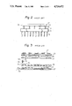
- FIG. 4 is an elevational, partially cross-sectional view of an embodiment of a package according to the present invention.
- a package 1 is provided with conductor pins 40 through conductor pads 3.
- the conductor pins 40 are brazed to the conductor pads 3.
- Elements the same as in FIG. 1A are denoted by the same reference numerals.
- the package of FIG. 4 is soldered through the conductor pins 40 to pads 9 provided on the top surface of the circuit board 2, as shown in FIG. 5A.
- FIG. 5B is an enlarged cross-sectional view of the connecting portions shown in FIG. 5A.
- the package 1 and the circuit board 2 have conductor pads 3 and 9 on the respective surface thereof.
- the conductor pads 3 of the package 1 are formed as a metallized layer during sintering of the ceramic substrate and are plated with nickel.
- the conductor pins 40 are brazed to the metallized conductor pads 3 with silver alloy 41, such as silver and copper, at a brazing temperature of 800° C. to 850° C.
- the conductor pins 40 are fixed to the surface of the conductor pads 3 in a substantially vertical contact condition.
- the surface of the conductor pads 3, conductor pins 40, and silver alloy 41 are generally plated with nickel and gold, i.e., two plating layers.
- the other conductor pads 3' are provided on the other side of the package. These are used for test pins.
- the conductor pins 40 are soldered to conductor pads 9 of the circuit board 2 using solder 42 at a well-known soldering temperature of, for example, 150° C. to 200° C.
- the conductor pads 9 consist of a copper layer plated with soft solder consisting of, for example, lead or tin alloy and the like.
- conductor pins 40 having a length of 0.5 to 1.5 mm and a diameter of 0.1 to 0.2 mm are preferably used.
- the conductor pins are preferably made of a low expansion coefficient alloy such as Iron-Nickel alloy, Iron-Nickel-Cobalt alloy, or tungsten, molybdenum, or copper alloy which have strengths of 200 g to 400 g/Iron-Nickel-Cobalt alloy pin.
- a low expansion coefficient alloy such as Iron-Nickel alloy, Iron-Nickel-Cobalt alloy, or tungsten, molybdenum, or copper alloy which have strengths of 200 g to 400 g/Iron-Nickel-Cobalt alloy pin.
- the structure shown in FIG. 4 has the merits that when the package is electrically connected to the circuit board or the like, the thermal stress generated during the operation of the assembly can be absorbed by the conductor pins 40 since they act as buffers of thermal stress. Thus, fractures of the connecting portions can be prevented.
- FIG. 6A is an elevational, partially cross-sectional view of another embodiment of a package according to the present invention.
- FIG. 6B is a schematic plan view of FIG. 6A.
- the semiconductor chip 5 is mounted on the base substrate 50 and the conductor pins 40 are provided on the same base substrate 50.
- the base substrate comprises a multi-layer ceramic substrate in which signal lines and through holes are provided for connection between the chip 5 and the conductor pins 40. Therefore, the conductor pins 40 can be provided on the entire back surface of the package 1.
- the conductor pins 40 are brazed to the conductor pads 3 as explained above.
- Such a package structure has the same effect as that explained in FIGS. 4 and 5A.
- the semiconductor device of the present invention has a structure in which the outer pins, e.g., conductor pins are electrically connected to the conductor pads 9 of the circuit board 2 under a contacting condition which is different from an inserted condition.
- the outer pins provided on the package are inserted into holes of the circuit board.
- using holes for insertion of the outer pins means a reduction of pin density and an increase of the package size.
- the present invention does not use the hole connection type but the contacting connection type which is the same as the leadless package, i.e., the chip carrier having outer pads, not pins, the density of the conductor pins is much higher than that of conventional packages. This means the size of the package can be small and also the density of the semiconductor device packages on the circuit board is high.
Landscapes
- Engineering & Computer Science (AREA)
- Manufacturing & Machinery (AREA)
- Microelectronics & Electronic Packaging (AREA)
- Lead Frames For Integrated Circuits (AREA)
Applications Claiming Priority (2)
| Application Number | Priority Date | Filing Date | Title |
|---|---|---|---|
| JP58-025858 | 1983-02-17 | ||
| JP58025858A JPS59151443A (ja) | 1983-02-17 | 1983-02-17 | 半導体装置 |
Related Parent Applications (1)
| Application Number | Title | Priority Date | Filing Date |
|---|---|---|---|
| US06579127 Continuation | 1984-02-10 |
Publications (1)
| Publication Number | Publication Date |
|---|---|
| US4724472A true US4724472A (en) | 1988-02-09 |
Family
ID=12177513
Family Applications (1)
| Application Number | Title | Priority Date | Filing Date |
|---|---|---|---|
| US07/006,347 Expired - Lifetime US4724472A (en) | 1983-02-17 | 1987-01-14 | Semiconductor device |
Country Status (4)
| Country | Link |
|---|---|
| US (1) | US4724472A (de) |
| EP (1) | EP0117111B1 (de) |
| JP (1) | JPS59151443A (de) |
| DE (1) | DE3484540D1 (de) |
Cited By (34)
| Publication number | Priority date | Publication date | Assignee | Title |
|---|---|---|---|---|
| US4963974A (en) * | 1985-10-14 | 1990-10-16 | Hitachi, Ltd. | Electronic device plated with gold by means of an electroless gold plating solution |
| US4970577A (en) * | 1988-04-12 | 1990-11-13 | Hitachi, Ltd. | Semiconductor chip module |
| US4982311A (en) * | 1987-09-29 | 1991-01-01 | Bull S.A. | Package for very large scale integrated circuit |
| US5041899A (en) * | 1988-06-08 | 1991-08-20 | Fujitsu Limited | Integrated circuit device having an improved package structure |
| US5046971A (en) * | 1988-12-14 | 1991-09-10 | Olin Corporation | Terminal pins for flexible circuits |
| US5057904A (en) * | 1988-03-18 | 1991-10-15 | Fujitsu Limited | Socket unit for package having pins and pads |
| US5097318A (en) * | 1988-04-04 | 1992-03-17 | Hitachi, Ltd. | Semiconductor package and computer using it |
| US5107329A (en) * | 1988-02-26 | 1992-04-21 | Hitachi, Ltd. | Pin-grid array semiconductor device |
| US5107328A (en) * | 1991-02-13 | 1992-04-21 | Micron Technology, Inc. | Packaging means for a semiconductor die having particular shelf structure |
| US5157479A (en) * | 1987-04-28 | 1992-10-20 | Sumitomo Electric Industries, Ltd. | Semiconductor device being capable of improving the packing density with a high heat radiation characteristics |
| US5170245A (en) * | 1988-06-15 | 1992-12-08 | International Business Machines Corp. | Semiconductor device having metallic interconnects formed by grit blasting |
| US5324892A (en) * | 1992-08-07 | 1994-06-28 | International Business Machines Corporation | Method of fabricating an electronic interconnection |
| US5379191A (en) * | 1991-02-26 | 1995-01-03 | Microelectronics And Computer Technology Corporation | Compact adapter package providing peripheral to area translation for an integrated circuit chip |
| US5393613A (en) * | 1991-12-24 | 1995-02-28 | Microelectronics And Computer Technology Corporation | Composition for three-dimensional metal fabrication using a laser |
| USRE34887E (en) * | 1986-06-06 | 1995-03-28 | Hitachi, Ltd. | Ceramic multilayer circuit board and semiconductor module |
| US5483421A (en) * | 1992-03-09 | 1996-01-09 | International Business Machines Corporation | IC chip attachment |
| US5490040A (en) * | 1993-12-22 | 1996-02-06 | International Business Machines Corporation | Surface mount chip package having an array of solder ball contacts arranged in a circle and conductive pin contacts arranged outside the circular array |
| US5536973A (en) * | 1993-05-28 | 1996-07-16 | Kabushiki Kaisha Toshiba | Semiconductor device including a semiconductor element mounted on a substrate using bump-shaped connecting electrodes |
| US5548486A (en) * | 1994-01-21 | 1996-08-20 | International Business Machines Corporation | Pinned module |
| US5574311A (en) * | 1994-01-28 | 1996-11-12 | Fujitsu Limited | Device having pins formed of hardened mixture of conductive metal particle and resin |
| US5633783A (en) * | 1994-09-29 | 1997-05-27 | Fujitsu Limited | Multi-chip ceramic module for mounting electric parts on both substrate and cap connected through interconnecting pins |
| US5675183A (en) * | 1995-07-12 | 1997-10-07 | Dell Usa Lp | Hybrid multichip module and methods of fabricating same |
| US5710459A (en) * | 1995-05-12 | 1998-01-20 | Industrial Technology Research Institute | Integrated circuit package provided with multiple heat-conducting paths for enhancing heat dissipation and wrapping around cap for improving integrity and reliability |
| US5859470A (en) * | 1992-11-12 | 1999-01-12 | International Business Machines Corporation | Interconnection of a carrier substrate and a semiconductor device |
| US5878483A (en) * | 1995-06-01 | 1999-03-09 | International Business Machines Corporation | Hammer for forming bulges in an array of compliant pin blanks |
| US5885853A (en) * | 1990-06-22 | 1999-03-23 | Digital Equipment Corporation | Hollow chip package and method of manufacture |
| US5889326A (en) * | 1996-02-27 | 1999-03-30 | Nec Corporation | Structure for bonding semiconductor device to substrate |
| US5892280A (en) * | 1994-03-11 | 1999-04-06 | Crane, Jr.; Stanford W. | Semiconductor chip carrier affording a high-density external interface |
| US5991160A (en) * | 1995-12-27 | 1999-11-23 | Infineon Technologies Corporation | Surface mount LED alphanumeric display |
| US6141869A (en) * | 1998-10-26 | 2000-11-07 | Silicon Bandwidth, Inc. | Apparatus for and method of manufacturing a semiconductor die carrier |
| US6543674B2 (en) | 2001-02-06 | 2003-04-08 | Fujitsu Limited | Multilayer interconnection and method |
| GB2396978B (en) * | 2002-11-18 | 2004-12-15 | Visteon Global Tech Inc | Electrical communications apparatus |
| US20050124184A1 (en) * | 2003-12-09 | 2005-06-09 | Xytrans, Inc. | Board-to-board connector |
| US20160343646A1 (en) * | 2015-05-21 | 2016-11-24 | Qualcomm Incorporated | High aspect ratio interconnect for wafer level package (wlp) and integrated circuit (ic) package |
Families Citing this family (6)
| Publication number | Priority date | Publication date | Assignee | Title |
|---|---|---|---|---|
| FR2622741A1 (fr) * | 1987-11-04 | 1989-05-05 | Nec Corp | Structure pour connexion de substrats a coefficients de dilatation thermique differents |
| JPH0741162Y2 (ja) * | 1989-10-26 | 1995-09-20 | 京セラ株式会社 | 半導体素子収納用パッケージ |
| JPH0363944U (de) * | 1989-10-26 | 1991-06-21 | ||
| JPH04256342A (ja) * | 1991-02-08 | 1992-09-11 | Toshiba Corp | 半導体パッケージ |
| JP3210503B2 (ja) * | 1993-09-30 | 2001-09-17 | 株式会社東芝 | マルチチップモジュールおよびその製造方法 |
| KR100416838B1 (ko) * | 2001-06-29 | 2004-02-05 | 주식회사 하이닉스반도체 | 반도체의 패키지장치 및 그 방법 |
Citations (4)
| Publication number | Priority date | Publication date | Assignee | Title |
|---|---|---|---|---|
| US3561107A (en) * | 1964-12-02 | 1971-02-09 | Corning Glass Works | Semiconductor process for joining a transistor chip to a printed circuit |
| EP0027017A1 (de) * | 1979-10-04 | 1981-04-15 | Fujitsu Limited | Kapselung für eine integrierte Halbleiterschaltung |
| US4338621A (en) * | 1980-02-04 | 1982-07-06 | Burroughs Corporation | Hermetic integrated circuit package for high density high power applications |
| JPS57181144A (en) * | 1981-05-01 | 1982-11-08 | Toshiba Corp | Semiconductor device |
Family Cites Families (2)
| Publication number | Priority date | Publication date | Assignee | Title |
|---|---|---|---|---|
| DE1234817B (de) * | 1963-12-27 | 1967-02-23 | Ibm | Mikroverbindung fuer auf eine mikroelektronische Schaltkarte aufzubringende Mikroschaltungs-elemente und Verfahren zu ihrer Herstellung |
| JPS5559746A (en) * | 1978-10-27 | 1980-05-06 | Hitachi Ltd | Semiconductor device and its mounting circuit device |
-
1983
- 1983-02-17 JP JP58025858A patent/JPS59151443A/ja active Pending
-
1984
- 1984-02-13 EP EP84300895A patent/EP0117111B1/de not_active Expired - Lifetime
- 1984-02-13 DE DE8484300895T patent/DE3484540D1/de not_active Expired - Lifetime
-
1987
- 1987-01-14 US US07/006,347 patent/US4724472A/en not_active Expired - Lifetime
Patent Citations (4)
| Publication number | Priority date | Publication date | Assignee | Title |
|---|---|---|---|---|
| US3561107A (en) * | 1964-12-02 | 1971-02-09 | Corning Glass Works | Semiconductor process for joining a transistor chip to a printed circuit |
| EP0027017A1 (de) * | 1979-10-04 | 1981-04-15 | Fujitsu Limited | Kapselung für eine integrierte Halbleiterschaltung |
| US4338621A (en) * | 1980-02-04 | 1982-07-06 | Burroughs Corporation | Hermetic integrated circuit package for high density high power applications |
| JPS57181144A (en) * | 1981-05-01 | 1982-11-08 | Toshiba Corp | Semiconductor device |
Non-Patent Citations (4)
| Title |
|---|
| IBM Technical Disclosure Bulletin, vol. 18, No. 5, Oct. 1975, "Flexible Solder Connection and Method of Fabricating", by P. Geldermans, pp. 1379-1380. |
| IBM TECHNICAL DISCLOSURE BULLETIN, vol. 18, no. 5, October 1975, pages 1379-1380, Armonk, US; P.GELDERMANS: "Flexible solder connection and method of fabricating" * |
| Patent Abstracts of Japan, vol. 7, No. 27, Feb. 1983. |
| PATENTS ABSTRACTS OF JAPAN, vol. 7, no. 27 (E-156)[1172], 3rd February 1983; & JP-A-57 181 144 (TOKYO SHIBAURA DENKI K.K.) 08-11-1982 * |
Cited By (45)
| Publication number | Priority date | Publication date | Assignee | Title |
|---|---|---|---|---|
| US4963974A (en) * | 1985-10-14 | 1990-10-16 | Hitachi, Ltd. | Electronic device plated with gold by means of an electroless gold plating solution |
| USRE34887E (en) * | 1986-06-06 | 1995-03-28 | Hitachi, Ltd. | Ceramic multilayer circuit board and semiconductor module |
| US5157479A (en) * | 1987-04-28 | 1992-10-20 | Sumitomo Electric Industries, Ltd. | Semiconductor device being capable of improving the packing density with a high heat radiation characteristics |
| US4982311A (en) * | 1987-09-29 | 1991-01-01 | Bull S.A. | Package for very large scale integrated circuit |
| US5107329A (en) * | 1988-02-26 | 1992-04-21 | Hitachi, Ltd. | Pin-grid array semiconductor device |
| US5057904A (en) * | 1988-03-18 | 1991-10-15 | Fujitsu Limited | Socket unit for package having pins and pads |
| US5097318A (en) * | 1988-04-04 | 1992-03-17 | Hitachi, Ltd. | Semiconductor package and computer using it |
| US4970577A (en) * | 1988-04-12 | 1990-11-13 | Hitachi, Ltd. | Semiconductor chip module |
| US5041899A (en) * | 1988-06-08 | 1991-08-20 | Fujitsu Limited | Integrated circuit device having an improved package structure |
| US5170245A (en) * | 1988-06-15 | 1992-12-08 | International Business Machines Corp. | Semiconductor device having metallic interconnects formed by grit blasting |
| US5046971A (en) * | 1988-12-14 | 1991-09-10 | Olin Corporation | Terminal pins for flexible circuits |
| US5885853A (en) * | 1990-06-22 | 1999-03-23 | Digital Equipment Corporation | Hollow chip package and method of manufacture |
| US5107328A (en) * | 1991-02-13 | 1992-04-21 | Micron Technology, Inc. | Packaging means for a semiconductor die having particular shelf structure |
| US5379191A (en) * | 1991-02-26 | 1995-01-03 | Microelectronics And Computer Technology Corporation | Compact adapter package providing peripheral to area translation for an integrated circuit chip |
| US5393613A (en) * | 1991-12-24 | 1995-02-28 | Microelectronics And Computer Technology Corporation | Composition for three-dimensional metal fabrication using a laser |
| US5483421A (en) * | 1992-03-09 | 1996-01-09 | International Business Machines Corporation | IC chip attachment |
| US5324892A (en) * | 1992-08-07 | 1994-06-28 | International Business Machines Corporation | Method of fabricating an electronic interconnection |
| US5920125A (en) * | 1992-11-12 | 1999-07-06 | International Business Machines Corporation | Interconnection of a carrier substrate and a semiconductor device |
| US5859470A (en) * | 1992-11-12 | 1999-01-12 | International Business Machines Corporation | Interconnection of a carrier substrate and a semiconductor device |
| US5536973A (en) * | 1993-05-28 | 1996-07-16 | Kabushiki Kaisha Toshiba | Semiconductor device including a semiconductor element mounted on a substrate using bump-shaped connecting electrodes |
| US5490040A (en) * | 1993-12-22 | 1996-02-06 | International Business Machines Corporation | Surface mount chip package having an array of solder ball contacts arranged in a circle and conductive pin contacts arranged outside the circular array |
| US5548486A (en) * | 1994-01-21 | 1996-08-20 | International Business Machines Corporation | Pinned module |
| CN1051409C (zh) * | 1994-01-21 | 2000-04-12 | 国际商业机器公司 | 销接组件 |
| US5715595A (en) * | 1994-01-21 | 1998-02-10 | International Business Machines Corporation | Method of forming a pinned module |
| US5574311A (en) * | 1994-01-28 | 1996-11-12 | Fujitsu Limited | Device having pins formed of hardened mixture of conductive metal particle and resin |
| US5843798A (en) * | 1994-01-28 | 1998-12-01 | Fujitsu Limited | Method for manufacturing semiconductor device having step of forming electrode pins on semiconductor chip using electrode-pin forming mask, and method for testing semiconductor chip using electrode-pin forming mask |
| US6097086A (en) * | 1994-03-11 | 2000-08-01 | Silicon Bandwidth, Inc. | Semiconductor chip carrier including an interconnect component interface |
| US20040007774A1 (en) * | 1994-03-11 | 2004-01-15 | Silicon Bandwidth, Inc. | Semiconductor chip carrier affording a high-density external interface |
| US5892280A (en) * | 1994-03-11 | 1999-04-06 | Crane, Jr.; Stanford W. | Semiconductor chip carrier affording a high-density external interface |
| US7183646B2 (en) | 1994-03-11 | 2007-02-27 | Silicon Bandwidth, Inc. | Semiconductor chip carrier affording a high-density external interface |
| US6577003B1 (en) | 1994-03-11 | 2003-06-10 | Silicon Bandwidth, Inc. | Semiconductor chip carrier affording a high-density external interface |
| US5633783A (en) * | 1994-09-29 | 1997-05-27 | Fujitsu Limited | Multi-chip ceramic module for mounting electric parts on both substrate and cap connected through interconnecting pins |
| US5710459A (en) * | 1995-05-12 | 1998-01-20 | Industrial Technology Research Institute | Integrated circuit package provided with multiple heat-conducting paths for enhancing heat dissipation and wrapping around cap for improving integrity and reliability |
| US5878483A (en) * | 1995-06-01 | 1999-03-09 | International Business Machines Corporation | Hammer for forming bulges in an array of compliant pin blanks |
| US5675183A (en) * | 1995-07-12 | 1997-10-07 | Dell Usa Lp | Hybrid multichip module and methods of fabricating same |
| US5991160A (en) * | 1995-12-27 | 1999-11-23 | Infineon Technologies Corporation | Surface mount LED alphanumeric display |
| US5889326A (en) * | 1996-02-27 | 1999-03-30 | Nec Corporation | Structure for bonding semiconductor device to substrate |
| US6857173B1 (en) | 1998-10-26 | 2005-02-22 | Silicon Bandwidth, Inc. | Apparatus for and method of manufacturing a semiconductor die carrier |
| US6141869A (en) * | 1998-10-26 | 2000-11-07 | Silicon Bandwidth, Inc. | Apparatus for and method of manufacturing a semiconductor die carrier |
| US6543674B2 (en) | 2001-02-06 | 2003-04-08 | Fujitsu Limited | Multilayer interconnection and method |
| GB2396978B (en) * | 2002-11-18 | 2004-12-15 | Visteon Global Tech Inc | Electrical communications apparatus |
| US7015869B2 (en) | 2002-11-18 | 2006-03-21 | Visteon Global Technologies, Inc. | High frequency antenna disposed on the surface of a three dimensional substrate |
| US20050124184A1 (en) * | 2003-12-09 | 2005-06-09 | Xytrans, Inc. | Board-to-board connector |
| US7086868B2 (en) * | 2003-12-09 | 2006-08-08 | Xytrans, Inc. | Board-to-board connector |
| US20160343646A1 (en) * | 2015-05-21 | 2016-11-24 | Qualcomm Incorporated | High aspect ratio interconnect for wafer level package (wlp) and integrated circuit (ic) package |
Also Published As
| Publication number | Publication date |
|---|---|
| DE3484540D1 (de) | 1991-06-13 |
| EP0117111A3 (en) | 1986-03-26 |
| EP0117111B1 (de) | 1991-05-08 |
| JPS59151443A (ja) | 1984-08-29 |
| EP0117111A2 (de) | 1984-08-29 |
Similar Documents
| Publication | Publication Date | Title |
|---|---|---|
| US4724472A (en) | Semiconductor device | |
| US5386341A (en) | Flexible substrate folded in a U-shape with a rigidizer plate located in the notch of the U-shape | |
| US6084777A (en) | Ball grid array package | |
| US6208025B1 (en) | Microelectronic component with rigid interposer | |
| US5668405A (en) | Semiconductor device with a film carrier tape | |
| US5942795A (en) | Leaded substrate carrier for integrated circuit device and leaded substrate carrier device assembly | |
| US5757071A (en) | C4 substrate contact pad which has a layer of Ni-B plating | |
| KR100231366B1 (ko) | 반도체 패키지 스택 모듈 및 그 제조방법 | |
| US6573609B2 (en) | Microelectronic component with rigid interposer | |
| JP2570637B2 (ja) | Mcmキャリア | |
| US5661337A (en) | Technique for improving bonding strength of leadframe to substrate in semiconductor IC chip packages | |
| US6054652A (en) | Thin-film multi-layer substrate and electronic device | |
| US4731700A (en) | Semiconductor connection and crossover apparatus | |
| JP2606603B2 (ja) | 半導体装置及びその製造方法及びその実装検査方法 | |
| US6351389B1 (en) | Device and method for packaging an electronic device | |
| JPH08191128A (ja) | 電子装置 | |
| JPH08236898A (ja) | 応力緩和用接続媒体、応力緩和型実装体及び応力緩和型部品 | |
| US20050073059A1 (en) | Integrated circuit with dual electrical attachment PAD configuration | |
| JPH07161866A (ja) | Lsiチップキャリア構造 | |
| WO1987004010A1 (en) | Chip interface mesa | |
| JPH05144971A (ja) | チツプキヤリア構造 | |
| JP3432552B2 (ja) | 窒化アルミニウム多層基板 | |
| JPS63229842A (ja) | 表面実装用パツケ−ジ | |
| JPS60138948A (ja) | 半導体装置用パツケ−ジ | |
| JP2001177038A (ja) | リードピン付き配線基板およびリードピン付き電子部品 |
Legal Events
| Date | Code | Title | Description |
|---|---|---|---|
| STCF | Information on status: patent grant |
Free format text: PATENTED CASE |
|
| FEPP | Fee payment procedure |
Free format text: PAYOR NUMBER ASSIGNED (ORIGINAL EVENT CODE: ASPN); ENTITY STATUS OF PATENT OWNER: LARGE ENTITY |
|
| FPAY | Fee payment |
Year of fee payment: 4 |
|
| FEPP | Fee payment procedure |
Free format text: PAYOR NUMBER ASSIGNED (ORIGINAL EVENT CODE: ASPN); ENTITY STATUS OF PATENT OWNER: LARGE ENTITY Free format text: PAYER NUMBER DE-ASSIGNED (ORIGINAL EVENT CODE: RMPN); ENTITY STATUS OF PATENT OWNER: LARGE ENTITY |
|
| FPAY | Fee payment |
Year of fee payment: 8 |
|
| FPAY | Fee payment |
Year of fee payment: 12 |