US4808549A - Method for fabricating a silicon force transducer - Google Patents
Method for fabricating a silicon force transducer Download PDFInfo
- Publication number
- US4808549A US4808549A US07/199,892 US19989288A US4808549A US 4808549 A US4808549 A US 4808549A US 19989288 A US19989288 A US 19989288A US 4808549 A US4808549 A US 4808549A
- Authority
- US
- United States
- Prior art keywords
- pair
- planar surface
- layer
- plate
- top planar
- Prior art date
- Legal status (The legal status is an assumption and is not a legal conclusion. Google has not performed a legal analysis and makes no representation as to the accuracy of the status listed.)
- Expired - Fee Related
Links
- 229910052710 silicon Inorganic materials 0.000 title claims abstract description 45
- 239000010703 silicon Substances 0.000 title claims abstract description 45
- XUIMIQQOPSSXEZ-UHFFFAOYSA-N Silicon Chemical compound [Si] XUIMIQQOPSSXEZ-UHFFFAOYSA-N 0.000 title claims abstract description 40
- 238000000034 method Methods 0.000 title claims description 27
- 239000000758 substrate Substances 0.000 claims abstract description 38
- 230000004044 response Effects 0.000 claims abstract description 23
- 238000005530 etching Methods 0.000 claims abstract description 22
- 239000004020 conductor Substances 0.000 claims abstract description 14
- VYPSYNLAJGMNEJ-UHFFFAOYSA-N Silicium dioxide Chemical compound O=[Si]=O VYPSYNLAJGMNEJ-UHFFFAOYSA-N 0.000 claims abstract description 13
- 239000000463 material Substances 0.000 claims abstract description 13
- 229910052814 silicon oxide Inorganic materials 0.000 claims abstract description 13
- 230000008859 change Effects 0.000 claims description 6
- 230000008878 coupling Effects 0.000 claims description 6
- 238000010168 coupling process Methods 0.000 claims description 6
- 238000005859 coupling reaction Methods 0.000 claims description 6
- ZOXJGFHDIHLPTG-UHFFFAOYSA-N Boron Chemical compound [B] ZOXJGFHDIHLPTG-UHFFFAOYSA-N 0.000 claims description 3
- 229910052796 boron Inorganic materials 0.000 claims description 3
- 239000004065 semiconductor Substances 0.000 claims 4
- 238000001704 evaporation Methods 0.000 claims 2
- 230000001590 oxidative effect Effects 0.000 claims 2
- 238000004544 sputter deposition Methods 0.000 claims 2
- 230000008901 benefit Effects 0.000 description 13
- 229910021420 polycrystalline silicon Inorganic materials 0.000 description 10
- 229920005591 polysilicon Polymers 0.000 description 10
- 230000035945 sensitivity Effects 0.000 description 9
- KWYUFKZDYYNOTN-UHFFFAOYSA-M Potassium hydroxide Chemical compound [OH-].[K+] KWYUFKZDYYNOTN-UHFFFAOYSA-M 0.000 description 7
- 238000013459 approach Methods 0.000 description 5
- 239000012212 insulator Substances 0.000 description 4
- 238000005452 bending Methods 0.000 description 3
- 238000006073 displacement reaction Methods 0.000 description 3
- 125000006850 spacer group Chemical group 0.000 description 3
- PIICEJLVQHRZGT-UHFFFAOYSA-N Ethylenediamine Chemical compound NCCN PIICEJLVQHRZGT-UHFFFAOYSA-N 0.000 description 2
- 239000002253 acid Substances 0.000 description 2
- 239000003990 capacitor Substances 0.000 description 2
- 238000000151 deposition Methods 0.000 description 2
- 238000010237 hybrid technique Methods 0.000 description 2
- 230000003993 interaction Effects 0.000 description 2
- 238000004518 low pressure chemical vapour deposition Methods 0.000 description 2
- 238000004519 manufacturing process Methods 0.000 description 2
- 238000005259 measurement Methods 0.000 description 2
- 229910052751 metal Inorganic materials 0.000 description 2
- 239000002184 metal Substances 0.000 description 2
- 238000013519 translation Methods 0.000 description 2
- XLYOFNOQVPJJNP-UHFFFAOYSA-N water Substances O XLYOFNOQVPJJNP-UHFFFAOYSA-N 0.000 description 2
- OAICVXFJPJFONN-UHFFFAOYSA-N Phosphorus Chemical compound [P] OAICVXFJPJFONN-UHFFFAOYSA-N 0.000 description 1
- 230000009471 action Effects 0.000 description 1
- 230000004075 alteration Effects 0.000 description 1
- 229910052782 aluminium Inorganic materials 0.000 description 1
- XAGFODPZIPBFFR-UHFFFAOYSA-N aluminium Chemical compound [Al] XAGFODPZIPBFFR-UHFFFAOYSA-N 0.000 description 1
- 229910052785 arsenic Inorganic materials 0.000 description 1
- RQNWIZPPADIBDY-UHFFFAOYSA-N arsenic atom Chemical compound [As] RQNWIZPPADIBDY-UHFFFAOYSA-N 0.000 description 1
- 238000005229 chemical vapour deposition Methods 0.000 description 1
- 239000013078 crystal Substances 0.000 description 1
- 230000008021 deposition Effects 0.000 description 1
- 238000009792 diffusion process Methods 0.000 description 1
- 239000012535 impurity Substances 0.000 description 1
- 150000002739 metals Chemical class 0.000 description 1
- 238000004377 microelectronic Methods 0.000 description 1
- 238000012986 modification Methods 0.000 description 1
- 230000004048 modification Effects 0.000 description 1
- 229910052698 phosphorus Inorganic materials 0.000 description 1
- 239000011574 phosphorus Substances 0.000 description 1
- 238000009877 rendering Methods 0.000 description 1
- 239000002210 silicon-based material Substances 0.000 description 1
Images


Classifications
-
- G—PHYSICS
- G01—MEASURING; TESTING
- G01L—MEASURING FORCE, STRESS, TORQUE, WORK, MECHANICAL POWER, MECHANICAL EFFICIENCY, OR FLUID PRESSURE
- G01L9/00—Measuring steady of quasi-steady pressure of fluid or fluent solid material by electric or magnetic pressure-sensitive elements; Transmitting or indicating the displacement of mechanical pressure-sensitive elements, used to measure the steady or quasi-steady pressure of a fluid or fluent solid material, by electric or magnetic means
- G01L9/0041—Transmitting or indicating the displacement of flexible diaphragms
- G01L9/0042—Constructional details associated with semiconductive diaphragm sensors, e.g. etching, or constructional details of non-semiconductive diaphragms
-
- G—PHYSICS
- G01—MEASURING; TESTING
- G01L—MEASURING FORCE, STRESS, TORQUE, WORK, MECHANICAL POWER, MECHANICAL EFFICIENCY, OR FLUID PRESSURE
- G01L1/00—Measuring force or stress, in general
- G01L1/14—Measuring force or stress, in general by measuring variations in capacitance or inductance of electrical elements, e.g. by measuring variations of frequency of electrical oscillators
- G01L1/142—Measuring force or stress, in general by measuring variations in capacitance or inductance of electrical elements, e.g. by measuring variations of frequency of electrical oscillators using capacitors
- G01L1/148—Measuring force or stress, in general by measuring variations in capacitance or inductance of electrical elements, e.g. by measuring variations of frequency of electrical oscillators using capacitors using semiconductive material, e.g. silicon
-
- H—ELECTRICITY
- H10—SEMICONDUCTOR DEVICES; ELECTRIC SOLID-STATE DEVICES NOT OTHERWISE PROVIDED FOR
- H10N—ELECTRIC SOLID-STATE DEVICES NOT OTHERWISE PROVIDED FOR
- H10N39/00—Integrated devices, or assemblies of multiple devices, comprising at least one piezoelectric, electrostrictive or magnetostrictive element covered by groups H10N30/00 – H10N35/00
-
- Y—GENERAL TAGGING OF NEW TECHNOLOGICAL DEVELOPMENTS; GENERAL TAGGING OF CROSS-SECTIONAL TECHNOLOGIES SPANNING OVER SEVERAL SECTIONS OF THE IPC; TECHNICAL SUBJECTS COVERED BY FORMER USPC CROSS-REFERENCE ART COLLECTIONS [XRACs] AND DIGESTS
- Y10—TECHNICAL SUBJECTS COVERED BY FORMER USPC
- Y10S—TECHNICAL SUBJECTS COVERED BY FORMER USPC CROSS-REFERENCE ART COLLECTIONS [XRACs] AND DIGESTS
- Y10S148/00—Metal treatment
- Y10S148/012—Bonding, e.g. electrostatic for strain gauges
Definitions
- the field of the invention relates to force transducers fabricated from silicon.
- sensitivity is inversely related to diaphragm thickness, and the diaphragm must be sufficiently thick to avoid both fracture and plate contact, there is a limit on the device sensitivity.
- Another problem is that because the diaphragm flexes or bends, deflection of the diaphragm is not rectilinear in response to the applied force. Thus, the required translation of diaghragm deflection into a measurement of the applied force is complicated. Still another problem is the fabricating complexity of bonding together two separate structures.
- U.S. Pat. No. 4,144,516 issued to Aine discloses adjacent folded cantilever leaf springs etched from a silicon substrate wherein leaf spring deflection is, allegedly, linearly proportional to the applied force.
- the disclosed device however still requires multiple substrates to be bonded together and it also appears to have limited sensitivity.
- U.S. Pat. No. 4,665,610 issued to Barth discloses a pressure transducer having multiple level diaphragms formed by etching a selectively etchable material, or spacer, between the diaphragm levels. This approach does not appear to provide rectilinear displacement of the diaghragm in response to the applied force. Another disadvantage is the inherent complexity in fabricating the multiple level diaphragms.
- An object of the invention is to provide a method for fabricating a force transducer from a single silicon substrate having parallel capacitive plates wherein plate movement is more nearly rectilinear in response to an applied force and the sensitivity of plate movement with respect to the applied force is greater than heretofore possible.
- the method includes the steps of: anisotropically etching parallel grooves along a top planar surface of a silicon substrate forming a first plate between the parallel grooves, preferably the silicon substrate has a ⁇ 100 ⁇ nominal plane so that the parallel grooves are V-shaped having side walls lying in the ⁇ 111 ⁇ planes; doping the top planar surface to form a conductive region, thereby rendering the first plate conductive without having to deposit a separate conducting plate on the top planar surface; forming a substantially uniform layer of a selectively etchable material over the grooved top planar surface; forming a substantially uniform layer of doped silicon over the layer of selectively etchable material following the contour of the grooved top planar surface to define a pair of corrugations opposite the pair of grooves and a second plate between the pair of corrugations, the corrugations preferably being V-shaped; etching a pair of openings through the silicon layer such that the second plate is connected to the silicon layer only through the pair of corrugations; applying
- the novel corrugations enhance plate deflections by the opening and closing of the corrugations.
- deflection of the plate is no-longer limited by the amount of flexing or bending the plate is able to withstand as is the case of prior approaches.
- the sensitivity of plate deflection may be further increased by increasing the number of corrugations.
- the corrugations are not constrained to be in a single plane, a large number of corrugations are obtained in a compact device. Advantages are thereby obtained of providing a force transducer having greater sensitivity and requiring less space than heretofore possible.
- the symmetrically placed corrugations with respect to the first plate also provide for a more nearly rectilinear deflection of the plate in response to an applied force as compared with prior approaches.
- Another advantage is that the entire structure is fabricated from a single silicon substrate.
- each plate is fabricated directly from a doped silicon material. An advantage is thereby obtained of eliminating the prior need of bonding conducting plates to a silicon substrate. A further advantage is that a separate insulator does not have to be bonded between two separate substrates.
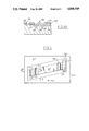
- FIG. 1 is a perspective view of an embodiment in which the invention is used to advantage
- FIG. 2 is a cross-sectional view taken along line 2--2 of FIG. 1;
- FIGS. 3A-3E illustrate various fabricating steps for fabricating the embodiment shown in FIG. 2;
- FIGS. 4A-4F illustrate various fabricating steps for fabricating an alternate embodiment in which the invention is used to advantage.
- FIG. 5 is a top planar view of the embodiment fabricated by the steps illustrated in FIGS. 4A-4F.
- force transducer 10 is shown in this example fabricated from a p-silicon substrate 12 having a top planar surface 14.
- Force transducer 10 includes first capacitive plate 16, shown as a portion of top planar surface 14 between V-grooves 18 and 20, and second capacitive plate 22, shown as a portion of p-doped polysilicon layer 24 suspended by corrugations 28 and 30.
- Top planar surface 14 and polysilicon layer 24 are shown separated by an insulator, silicon oxide layer 26 in this example.
- Both plate 16 and plate 22 are conductors fabricated from p-doped silicon as described in greater detail hereinafter.
- Electronic circuitry 32 measures the capacitive change between plates 16 and 22 which results from a deflection in plate 22 by an applied force.
- Corrugations 28 and 30 provide deflection of plate 22 by the accordian-like action of opening and closing in response to the applied force.
- movement of plate 22 occurs essentially by deflection of the corrugations rather than by flexure or bending of the plate itself.
- the sensitivity of plate movement in response to the applied force is easily increased by increasing the number of corrugations.
- the corrugations are not constrained to be in a single plane, a large number of corrugations are obtained in a compact device. Advantages are thereby obtained of providing a force transducer having greater sensitivity and requiring less space than heretofore possible.
- Corrugations 28 and 30 are also symmetrically positioned about plate 22. Therefore, plate 22 remains nearly planar regardless of the force applied. Stated another way, movement of plate 22 is rectilinear in response to the applied force. Translation of capacitance changes to a measurement of force is thereby simplified.
- FIGS. 3A through 3F an example of fabrication of force transducer 10 is presented.
- silicon substrate 12 having ⁇ 100 ⁇ nominal planes, is shown with a conventional silicon oxide mask 36 formed on top planar surface 14 by conventional photolithographic techniques.
- Mask 36 is shown having transverse openings 38 etched therethrough.
- an anisotropic etchant such as aqueous potassium hydroxide or ethylene diamine pyrocatecol and water solutions, is applied to openings 38 for forming first pair of V-grooves 18 and 20, and second pair of V-grooves 42 and 44.
- First pair of V-grooves 18 and 20 define a portion of capacitive plate 16 therebetween.
- the anisotropic etchant acts against the ⁇ 100 ⁇ nominal planes at a rate approximately 40 times greater than it acts against the intersecting ⁇ 111 ⁇ planes. Accordingly, V-grooves 18, 20, 42 and 44 are essentially defined by side walls lying in the ⁇ 111 ⁇ planes.
- mask 36 is chemically removed, in this example, by an etchant which acts against silicon oxide such as buffered hydroflouric acid.
- Substrate 12 is then surface-doped, with boron in this example, to form a p+ conductor region 46 (FIG. 3C).
- plate 16 becomes a conductive capacitor plate and the need for depositing a separate conductive plate on top planar surface 16 is eliminated.
- conductor region 46 extends along the entire top planar surface 14, the need for separate conductive traces to interconnect plate 16 with electronics circuitry 32 is eliminated.
- a selectively etchable layer 26 (FIG. 3D), silicon oxide in this example, is formed over grooved planar surface 14.
- selectively etchable layer 26 comprises a conventionally oxidized layer of silicon oxide in this example, it is to be noted that other selectively etchable materials may be used to advantage.
- p+ polysilicon layer 24 is deposited over selectively etchable layer 26 by use of conventional chemical vapor deposition techniques. It is noted that polysilicon layer 24 follows the contour of grooved planar surface 14 thereby forming corrugations 28 and 30, and second capacitive plate 22 therebetween. More specifically, corrugation 28 is shown in this example as the combination of V-shaped members 54 and 56 opposite respective V-grooves 42 and 18. V-shaped member 54 is shown defined by legs 58 and 60 positioned parallel to the side walls of V-groove 40. V-shaped member 56 is shown defined by legs 62 and 64 positioned parallel to the side walls of V-groove 18.
- corrugation 30 is shown in this example as the combination of V-shaped members 66 and 68 opposite respective V-grooves 20 and 44.
- V-shaped member 66 is shown defined by legs 70 and 72
- V-shaped member 68 is shown defined by legs 74 and 76.
- rectangular openings 80 and 82 are etched through polysilicon layer 24 in a longitudinal direction by an etchant, such as aqueous potassium hydroxide solution or ethylene diamine pyrocatecol and water solutions, thereby forming the transverse dimensions of plate 22, and corrugations 28 and 30.
- an etchant such as aqueous potassium hydroxide solution or ethylene diamine pyrocatecol and water solutions.
- the anisotropic etchant does not act against selectively etchable layer 26.
- an oxide etchant such as buffered hydroflouric acid
- corrugations 28 and 30 react in an accordian-like manner when a force to be measured, such as airflow, is applied to capacitive plate 22.
- V-shaped members 54 and 56 of corrugation 28, and V-shaped members 66 and 68 of corrugation 30 open or close thereby enabling displacement of capacitive plate 22 without flexure of capacitive plate 22.
- corrugations 28 and 30 are symmetrically positioned around capacitive plate 22.
- the opening and closing of both corrugation 28 and corrugation 30 in response to the applied force is virtually the same. Accordingly, displacement of capacitive plate 22 is nearly rectilinear in response to the applied force.
- conventional electronic circuitry 32 is shown connected, by conventional hybrid techniques, to both capacitive plate 16 and capacitive plate 22 by, respectively, p+ doped conductive region 46 and p+ doped polysilicon layer 24.
- Electronic circuitry 32 comprises conventional circuitry for measuring capacitive changes such as, for example, a capacitor bridge. Since both conductive region 46 and polysilicon layer 24 are p+ doped, conventional conductive strips, such as metal traces, between electronic circuitry 32 and both capacitive plates 16 and 22 are not needed. More specifically, electronic circuitry 32 is shown connected to capacitive plate 22 via a conductive lead, preferably aluminum, diffused into polysilicon layer 24. Similarly, electronic circuitry 32 is shown coupled to capacitive plate 16 via a conventional hole 86 formed through both polysilicon layer 24 and selectively etchable layer 26, and conductive trace 88 shown diffused into conductive region 46.
- force transducer 110 is shown in this example fabricated from an n-silicon substrate 112 with a selectively etchable layer, shown as a p-epitaxial layer, and a top silicon layer shown as a n-epitaxial layer.
- a selectively etchable layer shown as a p-epitaxial layer
- a top silicon layer shown as a n-epitaxial layer.
- the top silicon layer is crystalline due to interaction with the silicon substrate through the p-epitaxial layer which is also crystalline.
- the selectively etchable layer of the preceding embodiment is silicon oxide, interaction between the top silicon layer and substrate is prohibited resulting in a polycrystalline layer.
- An advantage of having a crystalline top layer is that electronic circuitry may be fabricated within the top layer without the need for hybrid techniques. A more detailed description for fabricating force transducer 110 is described hereinbelow.
- n-silicon wafer having ⁇ 100 ⁇ nominal planes is shown having silicon oxide mask 136 formed thereon.
- V-grooves 118, 120 (not shown), 142, and 144 are anisotropically etched into substrate 112 forming corrugations 128 and 130 (not shown), and also forming capacitive plate 116 between corrugations 118 and 120. That portion of substrate 112 which defines capacitive plate 116 is shown highly doped with an n-type impurity such as phosphorus or arsenic.
- silicon oxide pads 137 and 139 are formed by removing the appropriate portions of mask 136 by conventional photolithographic techniques.
- the selectively etchable layer is shown in this example as p-epitaxial layer 126 grown over substrate 112 and pads 137 and 139 (not shown) by low pressure chemical vapor deposition techniques (as described in A. C. Ipri, L. Jastrqebski and J. F. Corboy, proceedings, IEDM 82, p. 437).
- the portion of p-epitaxial layer 126 over pad 137 and pad 139 (not shown) is removed by conventional photolithographic and etching techniques.
- top silicon layer shown as n-epitaxial layer 124 in this example, is grown over p-epitaxial layer 126 and pad 137 and pad 139 (not shown) by low pressure chemical vapor deposition techniques.
- both p-epitaxial layer 126 and n-epitaxial layer 124 will have the same crystalographic orientation as substrate 112. Since both layers 124 and 126 have the same crystalographic orientation, a difficulty is presented in selectively etching layer 126 under layer 124 for suspending plate 122. This difficulty is overcome by the etchant steps described hereinbelow with particular reference to FIG. 5 and FIG. 4F.
- etchant opening 180 is shown anisotropically etched through n-epitaxial layer 124. Opening 180 is shown having longitudinal directions parallel to the ⁇ 110> crystal direction of the ⁇ 100 ⁇ substrate. Then using an electrochemical etching step (as described in Bell Systems Technical Journal, March 1970, Vol. 49, p. 473, by H. A. Waggener) n-epitaxial layer 124 and substrate 112 are biased positively (in a voltage range of 0.6 v to 1.0 v) and p-epitaxial layer 126 is at the voltage return.
- an anisotropic etchant such as aqeuous solution of KOH is applied to opening 180 to selectively etch a sufficient portion of p-epitaxial layer 126 to suspend both capacitive plate 122 and convolutions 128 and 130 (not shown) above substrate 112. It is noted that by orienting the longitudinal direction of opening 180 along some desired angle ⁇ with respect to the ⁇ 110> direction, selective etching of p-epitaxial layer 126 is enabled until intersection with the ⁇ 111] planes of layer 126.
- top layer is crystalline
- electronic circuitry 132 is fabricated directly within top layer 124 by conventional microelectronic techniques. Those skilled in the art will recognize that electronic circuitry 132 may be interconnected with capacitive plates 116 and 122 via electrically conductive strips formed by conventional deposition of appropriate insulators (not shown) and diffusion of appropriate metals (not shown).
- the symmetrical pair of corrugations which provides rectilinear movement of plate 22 may each comprise either single V-shaped members or multiple V-shaped members.
- capacitive plate 22 may totally comprise a plurality of corrugations. Accordingly, it is intended that the scope of the invention be limited only by the following claims.
Landscapes
- Physics & Mathematics (AREA)
- General Physics & Mathematics (AREA)
- Engineering & Computer Science (AREA)
- Power Engineering (AREA)
- Chemical & Material Sciences (AREA)
- Analytical Chemistry (AREA)
- Pressure Sensors (AREA)
- Measuring Fluid Pressure (AREA)
- Investigating Or Analyzing Materials By The Use Of Electric Means (AREA)
Priority Applications (4)
| Application Number | Priority Date | Filing Date | Title |
|---|---|---|---|
| US07/199,892 US4808549A (en) | 1988-05-27 | 1988-05-27 | Method for fabricating a silicon force transducer |
| DE89304025T DE68908953T2 (de) | 1988-05-27 | 1989-04-24 | Herstellungsverfahren eines Silizium-Kraftwandlers. |
| EP89304025A EP0343784B1 (de) | 1988-05-27 | 1989-04-24 | Herstellungsverfahren eines Silizium-Kraftwandlers |
| CA000600528A CA1288172C (en) | 1988-05-27 | 1989-05-24 | Method for fabricating a silicon force transducer |
Applications Claiming Priority (1)
| Application Number | Priority Date | Filing Date | Title |
|---|---|---|---|
| US07/199,892 US4808549A (en) | 1988-05-27 | 1988-05-27 | Method for fabricating a silicon force transducer |
Publications (1)
| Publication Number | Publication Date |
|---|---|
| US4808549A true US4808549A (en) | 1989-02-28 |
Family
ID=22739446
Family Applications (1)
| Application Number | Title | Priority Date | Filing Date |
|---|---|---|---|
| US07/199,892 Expired - Fee Related US4808549A (en) | 1988-05-27 | 1988-05-27 | Method for fabricating a silicon force transducer |
Country Status (4)
| Country | Link |
|---|---|
| US (1) | US4808549A (de) |
| EP (1) | EP0343784B1 (de) |
| CA (1) | CA1288172C (de) |
| DE (1) | DE68908953T2 (de) |
Cited By (27)
| Publication number | Priority date | Publication date | Assignee | Title |
|---|---|---|---|---|
| US4995953A (en) * | 1989-10-30 | 1991-02-26 | Motorola, Inc. | Method of forming a semiconductor membrane using an electrochemical etch-stop |
| WO1991014185A1 (en) * | 1990-03-08 | 1991-09-19 | Allied-Signal Inc. | Differential capacitive transducer and method of making |
| US5095401A (en) * | 1989-01-13 | 1992-03-10 | Kopin Corporation | SOI diaphragm sensor |
| EP0465573A4 (en) * | 1989-04-07 | 1992-08-12 | Ic Sensors, Inc. | Semiconductor transducer or actuator utilizing corrugated supports |
| US5145810A (en) * | 1990-06-25 | 1992-09-08 | Oki Electric Industry Co., Ltd. | Fabrication process of semiconductor pressure sensor for sensing pressure applied |
| US5177661A (en) * | 1989-01-13 | 1993-01-05 | Kopin Corporation | SOI diaphgram sensor |
| US5207866A (en) * | 1991-01-17 | 1993-05-04 | Motorola, Inc. | Anisotropic single crystal silicon etching solution and method |
| US5231878A (en) * | 1991-12-23 | 1993-08-03 | Ford Motor Company | Mass air flow sensor |
| US5286341A (en) * | 1990-04-14 | 1994-02-15 | Robert Bosch Gmbh | Process for producing micro-mechanical structures |
| US5314829A (en) * | 1992-12-18 | 1994-05-24 | California Institute Of Technology | Method for imaging informational biological molecules on a semiconductor substrate |
| US5313832A (en) * | 1991-12-23 | 1994-05-24 | Ford Motor Company | Composite mass air flow sensor |
| US5316619A (en) * | 1993-02-05 | 1994-05-31 | Ford Motor Company | Capacitive surface micromachine absolute pressure sensor and method for processing |
| US5360521A (en) * | 1993-11-12 | 1994-11-01 | Honeywell Inc. | Method for etching silicon |
| US5374792A (en) * | 1993-01-04 | 1994-12-20 | General Electric Company | Micromechanical moving structures including multiple contact switching system |
| US5407868A (en) * | 1992-12-08 | 1995-04-18 | Alliedsignal Inc. | Method of making an electrode tip for a tunnel current sensing device |
| US5484745A (en) * | 1993-10-26 | 1996-01-16 | Yazaki Meter Co., Ltd. | Method for forming a semiconductor sensor |
| US5490034A (en) * | 1989-01-13 | 1996-02-06 | Kopin Corporation | SOI actuators and microsensors |
| US5507911A (en) * | 1990-10-17 | 1996-04-16 | The Charles Stark Draper Laboratory, Inc. | Monolithic micromechanical vibrating string accelerometer with trimmable resonant frequency |
| US5578224A (en) * | 1995-06-07 | 1996-11-26 | Analog Devices, Inc. | Method of making micromachined device with ground plane under sensor |
| US5597767A (en) * | 1995-01-06 | 1997-01-28 | Texas Instruments Incorporated | Separation of wafer into die with wafer-level processing |
| US5674406A (en) * | 1993-11-02 | 1997-10-07 | Kyungpook National University Sensor Technology Research Center | Stopper manufacturing method of a silicon micromachining structure |
| US5943223A (en) * | 1997-10-15 | 1999-08-24 | Reliance Electric Industrial Company | Electric switches for reducing on-state power loss |
| US6007728A (en) * | 1997-08-14 | 1999-12-28 | Institute Of Micoelectronics | Design of a novel tactile sensor |
| US6013573A (en) * | 1996-02-23 | 2000-01-11 | Canon Kabushiki Kaisha | Method of manufacturing an air bridge type structure for supporting a micro-structure |
| US6284670B1 (en) * | 1997-07-23 | 2001-09-04 | Denso Corporation | Method of etching silicon wafer and silicon wafer |
| US6297069B1 (en) * | 1999-01-28 | 2001-10-02 | Honeywell Inc. | Method for supporting during fabrication mechanical members of semi-conductive dies, wafers, and devices and an associated intermediate device assembly |
| US20060196281A1 (en) * | 2005-03-02 | 2006-09-07 | Delphi Technologies, Inc. | Capacitive load cell apparatus having a non-planar nonconductive elastomeric dielectric |
Families Citing this family (4)
| Publication number | Priority date | Publication date | Assignee | Title |
|---|---|---|---|---|
| US6828171B2 (en) * | 2002-01-16 | 2004-12-07 | Xerox Corporation | Systems and methods for thermal isolation of a silicon structure |
| CN101069075B (zh) | 2004-12-08 | 2012-05-30 | Abb专利有限公司 | 制造测量变换器的方法 |
| EP1760037A1 (de) * | 2005-09-06 | 2007-03-07 | Infineon Technologies SensoNor AS | Verfahren zum Herstellen von mikromechanischen Strukturen |
| EP1760038B1 (de) * | 2005-09-06 | 2013-06-26 | Infineon Technologies AG | Verfahren zum Herstellen eines Masse-Feder Systems |
Citations (6)
| Publication number | Priority date | Publication date | Assignee | Title |
|---|---|---|---|---|
| US4071838A (en) * | 1976-02-09 | 1978-01-31 | Diax Corporation | Solid state force transducer and method of making same |
| US4144516A (en) * | 1976-03-29 | 1979-03-13 | Aine Harry E | Solid state transducer and method of making same |
| US4495820A (en) * | 1981-09-30 | 1985-01-29 | Hitachi, Ltd. | Capacitive pressure sensor |
| US4665610A (en) * | 1985-04-22 | 1987-05-19 | Stanford University | Method of making a semiconductor transducer having multiple level diaphragm structure |
| US4670969A (en) * | 1984-01-27 | 1987-06-09 | Hitachi, Ltd. | Method of making silicon diaphragm pressure sensor |
| US4773972A (en) * | 1986-10-30 | 1988-09-27 | Ford Motor Company | Method of making silicon capacitive pressure sensor with glass layer between silicon wafers |
Family Cites Families (2)
| Publication number | Priority date | Publication date | Assignee | Title |
|---|---|---|---|---|
| US4342227A (en) * | 1980-12-24 | 1982-08-03 | International Business Machines Corporation | Planar semiconductor three direction acceleration detecting device and method of fabrication |
| JPS6263828A (ja) * | 1985-09-06 | 1987-03-20 | Yokogawa Electric Corp | 振動式トランスジューサ |
-
1988
- 1988-05-27 US US07/199,892 patent/US4808549A/en not_active Expired - Fee Related
-
1989
- 1989-04-24 DE DE89304025T patent/DE68908953T2/de not_active Expired - Fee Related
- 1989-04-24 EP EP89304025A patent/EP0343784B1/de not_active Expired - Lifetime
- 1989-05-24 CA CA000600528A patent/CA1288172C/en not_active Expired - Lifetime
Patent Citations (6)
| Publication number | Priority date | Publication date | Assignee | Title |
|---|---|---|---|---|
| US4071838A (en) * | 1976-02-09 | 1978-01-31 | Diax Corporation | Solid state force transducer and method of making same |
| US4144516A (en) * | 1976-03-29 | 1979-03-13 | Aine Harry E | Solid state transducer and method of making same |
| US4495820A (en) * | 1981-09-30 | 1985-01-29 | Hitachi, Ltd. | Capacitive pressure sensor |
| US4670969A (en) * | 1984-01-27 | 1987-06-09 | Hitachi, Ltd. | Method of making silicon diaphragm pressure sensor |
| US4665610A (en) * | 1985-04-22 | 1987-05-19 | Stanford University | Method of making a semiconductor transducer having multiple level diaphragm structure |
| US4773972A (en) * | 1986-10-30 | 1988-09-27 | Ford Motor Company | Method of making silicon capacitive pressure sensor with glass layer between silicon wafers |
Cited By (31)
| Publication number | Priority date | Publication date | Assignee | Title |
|---|---|---|---|---|
| US5095401A (en) * | 1989-01-13 | 1992-03-10 | Kopin Corporation | SOI diaphragm sensor |
| US5177661A (en) * | 1989-01-13 | 1993-01-05 | Kopin Corporation | SOI diaphgram sensor |
| US5493470A (en) * | 1989-01-13 | 1996-02-20 | Kopin Corporation | SOI diaphragm sensor |
| US5490034A (en) * | 1989-01-13 | 1996-02-06 | Kopin Corporation | SOI actuators and microsensors |
| EP0465573A4 (en) * | 1989-04-07 | 1992-08-12 | Ic Sensors, Inc. | Semiconductor transducer or actuator utilizing corrugated supports |
| US4995953A (en) * | 1989-10-30 | 1991-02-26 | Motorola, Inc. | Method of forming a semiconductor membrane using an electrochemical etch-stop |
| EP0644427A1 (de) * | 1990-03-08 | 1995-03-22 | Endevco Corporation | Differentialkondensatormessumformer und Verfahren zu dessen Herstellung |
| WO1991014185A1 (en) * | 1990-03-08 | 1991-09-19 | Allied-Signal Inc. | Differential capacitive transducer and method of making |
| US5286341A (en) * | 1990-04-14 | 1994-02-15 | Robert Bosch Gmbh | Process for producing micro-mechanical structures |
| US5145810A (en) * | 1990-06-25 | 1992-09-08 | Oki Electric Industry Co., Ltd. | Fabrication process of semiconductor pressure sensor for sensing pressure applied |
| US5507911A (en) * | 1990-10-17 | 1996-04-16 | The Charles Stark Draper Laboratory, Inc. | Monolithic micromechanical vibrating string accelerometer with trimmable resonant frequency |
| US5207866A (en) * | 1991-01-17 | 1993-05-04 | Motorola, Inc. | Anisotropic single crystal silicon etching solution and method |
| US5231878A (en) * | 1991-12-23 | 1993-08-03 | Ford Motor Company | Mass air flow sensor |
| US5313832A (en) * | 1991-12-23 | 1994-05-24 | Ford Motor Company | Composite mass air flow sensor |
| US5407868A (en) * | 1992-12-08 | 1995-04-18 | Alliedsignal Inc. | Method of making an electrode tip for a tunnel current sensing device |
| US5314829A (en) * | 1992-12-18 | 1994-05-24 | California Institute Of Technology | Method for imaging informational biological molecules on a semiconductor substrate |
| US5454904A (en) * | 1993-01-04 | 1995-10-03 | General Electric Company | Micromachining methods for making micromechanical moving structures including multiple contact switching system |
| US5374792A (en) * | 1993-01-04 | 1994-12-20 | General Electric Company | Micromechanical moving structures including multiple contact switching system |
| US5316619A (en) * | 1993-02-05 | 1994-05-31 | Ford Motor Company | Capacitive surface micromachine absolute pressure sensor and method for processing |
| US5484745A (en) * | 1993-10-26 | 1996-01-16 | Yazaki Meter Co., Ltd. | Method for forming a semiconductor sensor |
| US5674406A (en) * | 1993-11-02 | 1997-10-07 | Kyungpook National University Sensor Technology Research Center | Stopper manufacturing method of a silicon micromachining structure |
| US5360521A (en) * | 1993-11-12 | 1994-11-01 | Honeywell Inc. | Method for etching silicon |
| US5597767A (en) * | 1995-01-06 | 1997-01-28 | Texas Instruments Incorporated | Separation of wafer into die with wafer-level processing |
| US5578224A (en) * | 1995-06-07 | 1996-11-26 | Analog Devices, Inc. | Method of making micromachined device with ground plane under sensor |
| US5828115A (en) * | 1995-06-07 | 1998-10-27 | Analog Devices, Inc. | Micromachined device with ground plane under sensor |
| US6013573A (en) * | 1996-02-23 | 2000-01-11 | Canon Kabushiki Kaisha | Method of manufacturing an air bridge type structure for supporting a micro-structure |
| US6284670B1 (en) * | 1997-07-23 | 2001-09-04 | Denso Corporation | Method of etching silicon wafer and silicon wafer |
| US6007728A (en) * | 1997-08-14 | 1999-12-28 | Institute Of Micoelectronics | Design of a novel tactile sensor |
| US5943223A (en) * | 1997-10-15 | 1999-08-24 | Reliance Electric Industrial Company | Electric switches for reducing on-state power loss |
| US6297069B1 (en) * | 1999-01-28 | 2001-10-02 | Honeywell Inc. | Method for supporting during fabrication mechanical members of semi-conductive dies, wafers, and devices and an associated intermediate device assembly |
| US20060196281A1 (en) * | 2005-03-02 | 2006-09-07 | Delphi Technologies, Inc. | Capacitive load cell apparatus having a non-planar nonconductive elastomeric dielectric |
Also Published As
| Publication number | Publication date |
|---|---|
| EP0343784A3 (de) | 1991-05-08 |
| DE68908953T2 (de) | 1994-01-05 |
| DE68908953D1 (de) | 1993-10-14 |
| EP0343784B1 (de) | 1993-09-08 |
| CA1288172C (en) | 1991-08-27 |
| EP0343784A2 (de) | 1989-11-29 |
Similar Documents
| Publication | Publication Date | Title |
|---|---|---|
| US4808549A (en) | Method for fabricating a silicon force transducer | |
| US4332000A (en) | Capacitive pressure transducer | |
| US4553436A (en) | Silicon accelerometer | |
| US4783237A (en) | Solid state transducer and method of making same | |
| US4236137A (en) | Semiconductor transducers employing flexure frames | |
| US4071838A (en) | Solid state force transducer and method of making same | |
| US5323656A (en) | Overpressure-protected, polysilicon, capacitive differential pressure sensor and method of making the same | |
| US4050049A (en) | Solid state force transducer, support and method of making same | |
| US5060526A (en) | Laminated semiconductor sensor with vibrating element | |
| JP3114570B2 (ja) | 静電容量型圧力センサ | |
| US4016644A (en) | Methods of fabricating low pressure silicon transducers | |
| JP3457037B2 (ja) | 集積型加速度計 | |
| US4467656A (en) | Transducer apparatus employing convoluted semiconductor diaphragms | |
| US4597003A (en) | Chemical etching of a semiconductive wafer by undercutting an etch stopped layer | |
| US4605919A (en) | Piezoresistive transducer | |
| US4812199A (en) | Rectilinearly deflectable element fabricated from a single wafer | |
| CN101111751A (zh) | 压阻应变集中器 | |
| US5589810A (en) | Semiconductor pressure sensor and related methodology with polysilicon diaphragm and single-crystal gage elements | |
| CN113218544B (zh) | 具有应力集中结构的微压传感器芯片及其制备方法 | |
| US4025942A (en) | Low pressure transducers employing large silicon diaphragms having non-critical electrical properties | |
| CN109246565A (zh) | 硅麦克风及其制造方法 | |
| US4737473A (en) | Piezoresistive transducer | |
| US6051855A (en) | Electrostatic capacitive sensor | |
| CN224136763U (zh) | 一种半导体应变计和压力传感器 | |
| JPH07318445A (ja) | 静電容量型圧力センサとその製造方法 |
Legal Events
| Date | Code | Title | Description |
|---|---|---|---|
| AS | Assignment |
Owner name: FORD MOTOR COMPANY, DEARBORN, MICHIGAN, A CORP. OF Free format text: ASSIGNMENT OF ASSIGNORS INTEREST.;ASSIGNORS:MIKKOR, MATI;SICKAFUS, EDWARD N.;REEL/FRAME:004938/0892 Effective date: 19880520 |
|
| FEPP | Fee payment procedure |
Free format text: PAYOR NUMBER ASSIGNED (ORIGINAL EVENT CODE: ASPN); ENTITY STATUS OF PATENT OWNER: LARGE ENTITY |
|
| FPAY | Fee payment |
Year of fee payment: 4 |
|
| REMI | Maintenance fee reminder mailed | ||
| LAPS | Lapse for failure to pay maintenance fees | ||
| FP | Lapsed due to failure to pay maintenance fee |
Effective date: 19970305 |
|
| STCH | Information on status: patent discontinuation |
Free format text: PATENT EXPIRED DUE TO NONPAYMENT OF MAINTENANCE FEES UNDER 37 CFR 1.362 |