US4900989A - Magnetron feeding apparatus and method of controlling the same - Google Patents
Magnetron feeding apparatus and method of controlling the same Download PDFInfo
- Publication number
- US4900989A US4900989A US07/189,166 US18916688A US4900989A US 4900989 A US4900989 A US 4900989A US 18916688 A US18916688 A US 18916688A US 4900989 A US4900989 A US 4900989A
- Authority
- US
- United States
- Prior art keywords
- output voltage
- input current
- information
- magnetron
- given value
- Prior art date
- Legal status (The legal status is an assumption and is not a legal conclusion. Google has not performed a legal analysis and makes no representation as to the accuracy of the status listed.)
- Expired - Lifetime
Links
Images


Classifications
-
- H—ELECTRICITY
- H05—ELECTRIC TECHNIQUES NOT OTHERWISE PROVIDED FOR
- H05B—ELECTRIC HEATING; ELECTRIC LIGHT SOURCES NOT OTHERWISE PROVIDED FOR; CIRCUIT ARRANGEMENTS FOR ELECTRIC LIGHT SOURCES, IN GENERAL
- H05B6/00—Heating by electric, magnetic or electromagnetic fields
- H05B6/64—Heating using microwaves
- H05B6/70—Feed lines
-
- H—ELECTRICITY
- H05—ELECTRIC TECHNIQUES NOT OTHERWISE PROVIDED FOR
- H05B—ELECTRIC HEATING; ELECTRIC LIGHT SOURCES NOT OTHERWISE PROVIDED FOR; CIRCUIT ARRANGEMENTS FOR ELECTRIC LIGHT SOURCES, IN GENERAL
- H05B6/00—Heating by electric, magnetic or electromagnetic fields
- H05B6/64—Heating using microwaves
- H05B6/66—Circuits
- H05B6/666—Safety circuits
-
- H—ELECTRICITY
- H02—GENERATION; CONVERSION OR DISTRIBUTION OF ELECTRIC POWER
- H02M—APPARATUS FOR CONVERSION BETWEEN AC AND AC, BETWEEN AC AND DC, OR BETWEEN DC AND DC, AND FOR USE WITH MAINS OR SIMILAR POWER SUPPLY SYSTEMS; CONVERSION OF DC OR AC INPUT POWER INTO SURGE OUTPUT POWER; CONTROL OR REGULATION THEREOF
- H02M3/00—Conversion of DC power input into DC power output
- H02M3/22—Conversion of DC power input into DC power output with intermediate conversion into AC
- H02M3/24—Conversion of DC power input into DC power output with intermediate conversion into AC by static converters
- H02M3/28—Conversion of DC power input into DC power output with intermediate conversion into AC by static converters using discharge tubes with control electrode or semiconductor devices with control electrode to produce the intermediate AC
- H02M3/325—Conversion of DC power input into DC power output with intermediate conversion into AC by static converters using discharge tubes with control electrode or semiconductor devices with control electrode to produce the intermediate AC using devices of a triode or a transistor type requiring continuous application of a control signal
- H02M3/335—Conversion of DC power input into DC power output with intermediate conversion into AC by static converters using discharge tubes with control electrode or semiconductor devices with control electrode to produce the intermediate AC using devices of a triode or a transistor type requiring continuous application of a control signal using semiconductor devices only
- H02M3/33507—Conversion of DC power input into DC power output with intermediate conversion into AC by static converters using discharge tubes with control electrode or semiconductor devices with control electrode to produce the intermediate AC using devices of a triode or a transistor type requiring continuous application of a control signal using semiconductor devices only with automatic control of the output voltage or current, e.g. flyback converters
- H02M3/33523—Conversion of DC power input into DC power output with intermediate conversion into AC by static converters using discharge tubes with control electrode or semiconductor devices with control electrode to produce the intermediate AC using devices of a triode or a transistor type requiring continuous application of a control signal using semiconductor devices only with automatic control of the output voltage or current, e.g. flyback converters with galvanic isolation between input and output of both the power stage and the feedback loop
-
- H—ELECTRICITY
- H02—GENERATION; CONVERSION OR DISTRIBUTION OF ELECTRIC POWER
- H02M—APPARATUS FOR CONVERSION BETWEEN AC AND AC, BETWEEN AC AND DC, OR BETWEEN DC AND DC, AND FOR USE WITH MAINS OR SIMILAR POWER SUPPLY SYSTEMS; CONVERSION OF DC OR AC INPUT POWER INTO SURGE OUTPUT POWER; CONTROL OR REGULATION THEREOF
- H02M7/00—Conversion of AC power input into DC power output; Conversion of DC power input into AC power output
- H02M7/42—Conversion of DC power input into AC power output without possibility of reversal
- H02M7/44—Conversion of DC power input into AC power output without possibility of reversal by static converters
- H02M7/48—Conversion of DC power input into AC power output without possibility of reversal by static converters using discharge tubes with control electrode or semiconductor devices with control electrode
- H02M7/53—Conversion of DC power input into AC power output without possibility of reversal by static converters using discharge tubes with control electrode or semiconductor devices with control electrode using devices of a triode or transistor type requiring continuous application of a control signal
- H02M7/537—Conversion of DC power input into AC power output without possibility of reversal by static converters using discharge tubes with control electrode or semiconductor devices with control electrode using devices of a triode or transistor type requiring continuous application of a control signal using semiconductor devices only, e.g. single switched pulse inverters
-
- H—ELECTRICITY
- H03—ELECTRONIC CIRCUITRY
- H03B—GENERATION OF OSCILLATIONS, DIRECTLY OR BY FREQUENCY-CHANGING, BY CIRCUITS EMPLOYING ACTIVE ELEMENTS WHICH OPERATE IN A NON-SWITCHING MANNER; GENERATION OF NOISE BY SUCH CIRCUITS
- H03B9/00—Generation of oscillations using transit-time effects
- H03B9/01—Generation of oscillations using transit-time effects using discharge tubes
- H03B9/10—Generation of oscillations using transit-time effects using discharge tubes using a magnetron
-
- H—ELECTRICITY
- H05—ELECTRIC TECHNIQUES NOT OTHERWISE PROVIDED FOR
- H05B—ELECTRIC HEATING; ELECTRIC LIGHT SOURCES NOT OTHERWISE PROVIDED FOR; CIRCUIT ARRANGEMENTS FOR ELECTRIC LIGHT SOURCES, IN GENERAL
- H05B6/00—Heating by electric, magnetic or electromagnetic fields
- H05B6/64—Heating using microwaves
- H05B6/66—Circuits
- H05B6/68—Circuits for monitoring or control
Definitions
- the present invention generally relates to improvements in a high-frequency heating apparatus for heating food, liquid or the like by a so-called dielectric heating, and more particularly, to a magnetron feeding apparatus and a method of controlling the magnetron feeding apparatus which is adapted to effect a feeding operation to a magnetron by an inverter circuit using a semiconductor switch and a high-tension transformer.
- a magnetron feeding apparatus shown in FIG. 1 is adapted to convert a DC current 2 from a power supply portion 1 into high-frequency power 5 by an inverter circuit 4 using a semiconductor switch 3 such as a transistor, and furthermore to convert into high-tension power 7 by a high-tension transformer 6 to feed the power to a magnetron 8.
- a method of controlling the feeding power comprises steps of detecting the input current from a commercial power supply 9 by an input detecting portion 10, and forming the difference 12 between its value and a reference signal 11 by an error amplification circuit 13; a driving circuit 14 generates a driving pulse 15 corresponding to the difference 12 so as to turn the semiconductor switch on and off, so that the input current is controlled to be a given value.
- the power feeding operation will be approximately one-seventh of feed power at the steady-state time when the magnetron 8 is oscillating.
- the reference signal 11 is set to a value smaller at the steady-state time before the magnetron 8 starts its oscillation so as to be controlled to small input current which is proper to the heater heating operation.
- the reference signal 11 is switched to the value at the steady-state time after the lapse of the time sufficient enough for the magnetron 8 to start its oscillation, so that the input current may be controlled to a value at the steady-state time.
- the time for the timer 16 is set as five seconds for safety.
- an essential object of the present invention is to provide a magnetron feeding apparatus, which is capable of controlling the output voltage of the high-tension transformer and the input current to the inverter circuit.
- Another important object of the present invention is to provide a magnetron feeding apparatus which is capable of reaching so far as the oscillable condition of the magnetron within a shorter time, because a large voltage, i.e., as much power as is possible may be provided without the application of excessive voltage to the magnetron in a period before the magnetron starts its oscillation, namely, when the output voltage of the high-tension transformer is large in spite of a small input current to the inverter circuit.
- a further object of the present invention is to provide a magnetron feeding apparatus of the above-described type in which the controlling operation is effected so that the input current may reach its given value with the result that the starting operation may be effected without consumption of a wasteful time to the oscillating condition of the magnetron or the oscillating condition may be stably continued, because the input current to the inverter circuit is rapidly increased although the output voltage of the high-tension transformer has an excessive voltage for one second or less, with the magnetron being an extremely low impedance load under constant application of voltage when the oscillable condition is reached.
- a magnetron feeding apparatus which includes a power-supply portion for feeding DC current, an inverter circuit for converting the DC power into high-frequency power by the switching operation of a semiconductor switch, a high-tension transformer for converting the high-frequency power into high-tension power to be supplied to the magnetron, an output voltage detector for detecting the output voltage of the high-tension transformer, an input current detector for detecting the input current to the converter circuit, a power controller for controlling the switching operation of the semiconductor switch in response to the output voltage detected by the output voltage detector and the input current detected by the input current detector.
- an improved magnetron feeding apparatus removes the above-described wasteful time without lowering the service life of the magnetron.
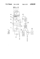
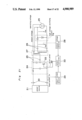
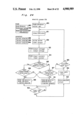
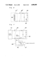
- FIG. 1 is a block diagram of a conventional magnetron feeding apparatus
- FIG. 2 is a construction conceptional diagram of a magnetron feeding apparatus of the present invention
- FIG. 3 is a block diagram of a first embodiment of an output voltage detector of the present invention.
- FIG. 4 is a block diagram of a second embodiment of an output voltage detector of the present invention.
- FIG. 5 is a block diagram of a first embodiment of a power supply of the present invention.
- FIG. 6 is a block diagram of a second embodiment of a power supply of the present invention.
- FIG. 7 is a block diagram of a first embodiment of an input current detector of the present invention.
- FIG. 8 is a block diagram of a second embodiment of an input current detector of the present invention.
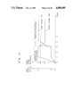
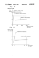
- FIG. 9 shows a simple equivalent circuit of a magnetron
- FIG. 10 shows a characteristic graph of a magnetron
- FIG. 11 shows a characteristic graph of a magnetron feeding apparatus
- FIG. 12 is a block diagram of a first embodiment of a power controller of the present invention.
- FIG. 13 shows a start characteristic graph of a magnetron feeding apparatus
- FIG. 14 is a block diagram of another embodiment of a first reference signal generating circuit of the present invention.
- FIG. 15 is a block diagram of a first gradual increasing circuit
- FIG. 16 is a block diagram of another embodiment of a power controller of the present invention which is partially changed from the controller shown in FIG. 13;
- FIG. 17 is a characteristic graph thereof
- FIG. 18 is a block diagram of a second embodiment of a power controller of the present invention.
- FIG. 19 is a block diagram of a third embodiment of a power controller of the present invention.
- FIG. 20 is a characteristic graph of a magnetron feeding apparatus in this case.
- FIG. 21 is the other construction conventional diagram of a magnetron feeding apparatus
- FIG. 22 is a circuit block diagram of a magnetron feeding apparatus when the power controlling operation is performed by the software processing operation
- FIG. 23 is a conceptional diagram of a program flow of a software processing portion
- FIG. 24 is a flowchart of a first embodiment of a software processing portion of the present invention.
- FIG. 25 is a flowchart of a second embodiment of a software processing portion of the present invention.
- FIG. 26 is a flowchart of a third embodiment of a software processing portion of the present invention.
- FIG. 2 a magnetron feeding apparatus of the present invention, which includes a power supply 21 for feeding DC current 20, an inverter circuit 24 which switches in high frequency the DC power supply 20 by a semiconductor switch 22 to convert it into high-frequency power 23, a high-tension transformer 27 which converts the high-frequency power 23 into the high-tension power 26 necessary for the operation of a magnetron 25, an output voltage detector 28 which detects the output voltage V OUT of the high-tension transformer 27, an input current detector 29 which detects the input current I IN into the inverter circuit 24, a power controller 33 for controlling the switching operation of an inverter circuit 24 through the outputting of driving pulses 32 which turn the semiconductor switch 22 on and off using the output voltage 30 of the output voltage detector 28 and the input current 31 of the input current detector 29.
- a power supply 21 for feeding DC current 20
- an inverter circuit 24 which switches in high frequency the DC power supply 20 by a semiconductor switch 22 to convert it into high-frequency power 23
- a high-tension transformer 27 which converts the high-frequency power 23
- FIG. 3 is a construction diagram of a first embodiment of an output voltage detector 28'.
- an exclusive detection winding 34 is provided on the output (secondary) side of the high-tension transformer 27', with the output thereof being adapted to be outputted by the conversion into the output 30' through a first rectification circuit 35.
- the output voltage 30' corresponding to the output voltage V OUT may be provided.
- FIG. 4 is a construction diagram of a second embodiment of an output voltage detector 28".
- a detecting winding 36 which uses in combination one portion of the winding of the output (secondary) side of the high-tension transformer 27" is provided, with the output thereof being adapted to be outputted by the conversion into the output voltage 30" corresponding to the output voltage V OUT through a second rectification circuit 37.
- FIG. 5 is a construction diagram of a first embodiment of a power supply 21'.
- the DC power 20' to be fed to the inverter circuit 24 is adapted to get commercial power 38 through a third rectification circuit 39.
- FIG. 6 is a construction diagram showing a second embodiment of a power-supply 21". Referring to FIG. 6, DC current 20" to be fed to the inverter circuit 24 is adapted to be provided from a battery 40.
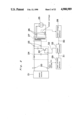
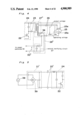
- FIG. 7 is a block diagram showing the first embodiment of an input current detector 29'.
- a current detection resistor 41 is inserted into between the power supply 21 and the inverter circuit 24 so as to convert the voltage across the ends thereof into an input current 31' through a fourth rectification circuit 42 so that information corresponding to the input current I IN may be inputted.
- FIG. 8 is a construction diagram showing the second embodiment of an input current detector 29".
- the primary winding 43 P of a current detection transformer 43 is inserted into a commercial power supply 38 and a third rectification circuit 39 to convert the voltage in the secondary winding 43 S into an input current 31" through a fifth rectification circuit 44 so that the information corresponding to the input current I IN may be outputted.
- a magnetron 25, which is a feeding object of a magnetron feeding apparatus of the present invention, will be described hereinafter.
- FIG. 9 shows a single equivalent circuit of a magnetron 25.
- an equivalence between the anode 25 A and the cathode 25 K may be obtained by a resistor 25R, a variable resistor 25V R and a Zener diode 25V Z .
- the value of the variable resistor 25V R is changed through the heating operation of a heater 25 H . (V R value during non-heating of the heater 25 H )/(V R value during heating of the heater 25 H ) becomes a value of 100 or more, so that the magnetron 25 oscillates at a high frequency during the heating operation of the heater 25 H .
- the relationship between the operating voltage: V AK to be applied between the anode 25 A of the magnetron 25 and the cathode 25 K , and the operating current: I AK becomes a load equivalent to the resistance of the high impedance when the magnetron 25 is not oscillating, and a load equivalent to a Zener diode of a low impedance when the magnetron 25 is oscillating as shown in the characteristic graph of FIG. 10.
- FIG. 11 is an input, output characteristic graph of the magnetron feeding apparatus showing the relationship between the input current: I IN of an inverter circuit which feeds power to such a magnetron 25 and the output voltage V OUT of the high-tension transformer.
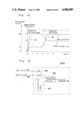
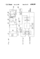
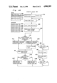
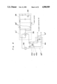
- FIG. 12 is a block diagram showing the first embodiment of a power controller 33'.
- a first diode circuit 45 inputs the larger of the output voltage 30 and the input current 31 into a first error amplification circuit 46.
- the first error amplification circuit 46 outputs a difference signal 48 between this input and the output of a first reference signal generating circuit 47.
- a first comparator 49 outputs a driving pulse 32' which turns the semiconductor switch 22 on and off in accordance with the difference signal 48 and a saw-tooth wave 51 from a first saw-tooth wave generating circuit 50.
- the output voltage 30 increases with decreases in the output of the first error amplification circuit 46, so that the on time of the driving pulse 32' decreases to lower the output voltage V OUT . Inversely, when the output voltage 30 decreases, the on time of the driving pulse 32' increases to make the output voltage V OUT increase.
- the output in the first error amplification circuit 46 is reduced to decrease the on time of the driving pulse 32', so that the operation is effected in such a direction as to reduce the input current I IN .
- the on time of the driving pulse 32' is increased, so that the operation is effected in such a way as to increase the input current I IN .
- a second reference signal generating circuit 53 is provided which is equivalent to, for example 6 KVo-p if the output voltage V OUT is 6 KVo-p or more, and which is turned on when the output voltage V OUT is 6 KVo-p or lower, so that the input current I IN may be gradually increased if the output voltage V OUT ⁇ 6 KVo-p as shown in FIG. 17.
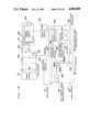
- FIG. 18 is a block diagram showing a second embodiment of a power controller 33".
- a second error amplification circuit 55 outputs a difference signal 57 between the output voltage 30 and the reference signal of a third reference signal generating circuit 56 to a second diode circuit 58.
- a third error amplification circuit 59 outputs a difference signal 61 between the input current 31 and the reference signal of a fourth reference signal generating circuit 60 to a second diode circuit 58.
- the second diode 58 outputs to a third comparator 62 the smaller of the two difference signals 57 and 61.
- the third comparator 62 outputs a driving pulse 32" which turns the semiconductor switch 22 on and off by the input and the sawtooth wave 64 from the second sawtooth wave generating circuit 63.
- the required input current I IN when the output voltage V OUT is 7 KVo-p as shown in FIG. 11 is approximately 2 A , so that the difference signal 61 from the third error amplification circuit 59 becomes larger than the difference signal 57 from the second error amplification circuit 55.
- the required input current I IN is less, i.e., the difference signal 57 from the second error amplification circuit 55 is selectively outputted by a second diode circuit 58.
- the output of the second error amplification circuit 55 is decreased to reduce the on time of the driving pulse 32", so that the operation is effected in such a direction as to decrease the output voltage V OUT .
- the on time of the driving pulse 32" increases so that the operation is operated in such a direction as to increase the output voltage V OUT .
- the output voltage V OUT when the input current I IN is approximately 4 KVo-p as shown in FIG. 11, so that the difference signal 57 from the second error amplification circuit 55 becomes larger than the difference signal 61 from the third error amplification circuit 59.
- the required input current I IN is small, i.e., the difference signal from the third error amplification circuit 59 is selectively outputted by the diode circuit 58.
- the output of the third error amplification 59 decreases to reduce the on time of the driving pulse 32", so that the operation is effected in such a direction as to reduce the input current I IN .
- the operation is effected in such a way as to increase to make the input current I IN more through the increase of the on time of the driving pulse 32".
- the starting characteristics becomes the same as those of the starting characteristics graph of the first embodiment shown in FIG. 13.
- the third reference signal generating circuit 56 is constructed to have the time constant of the above-described FIG. 14, so that the controlling operation may be performed so as to gradually increase the output voltage V OUT up to 7 KV as shown in the dotted line A of FIG. 13.
- the first gradual increasing circuit 52 shown in FIG. 15 is inserted into between the second diode circuit 58 and the third comparator 62, so that the controlling operation may be controlled so as to gradually increase the output voltage V OUT and the input current I IN as in the dotted line A of FIG. 13 and the dotted line thereof.
- the first gradual increasing circuit 52 is inserted into between the second diode circuit 58 and the third comparator 62.
- the first gradual increasing circuit 52 is turned on and off in accordance with the output voltage 30 as shown in FIG. 16 to gradually increase the input current I IN .
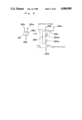
- FIG. 19 is a block diagram showing a third embodiment of the power controller portion 33"'.
- a fourth error amplification circuit 65 outputs to a fourth comparator 69 a difference signal 68 between the reference signal from a fifth reference signal generating circuit 67 passing through the gradual increasing, gradual decreasing circuit 66, and the input current 31.
- the fourth comparator 69 outputs a driving pulse 32" which switches the semiconductor switch 22 on and off through the difference signal 68 and the sawtooth wave 71 from the third sawtooth wave generating circuit 70.
- the output voltage V OUT is approximately 4 KVo-p , with the switch 72s being off.
- the input current 31 increases, the output of the fourth error amplification circuit 65 is decreased to reduce the on time of the driving pulse 32" so that the operation is effected in such a direction as to reduce the input current I IN .
- the on time of the driving pulse 32" is decreased so that an operation is effected in such a way as to increase the input current I IN .
- FIG. 20 is a characteristic graph of a magnetron feeding apparatus in such a condition as described hereinabove.
- the output voltage V OUT increases up to 7 KVo-p , thereafter minutely vibrates around 7 KVo-p and the input current I IN increases up to 12 A and then is controlled so as to be constant.
- FIG. 21 is a construction conceptional diagram of a magnetron feeding apparatus when a high-tension rectification circuit 74 is inserted into between the high-tension transformer 27 and the magnetron 25.
- the sensitivity of the output voltage detector 28 is required to be approximately doubled as the output voltage V OUT is different in value from the operatively voltage V AK . Accordingly, the power controller 33 may be realized in terms of the operation similar to the above-described operation even in a magnetron feeding apparatus equipped with a high-tension rectification circuit 74.
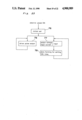
- FIG. 22 is a circuit block diagram in a case where the power control of the magnetron feeding apparatus is effected by the software processing.
- the software processing portion 75 inputs the input current 31 from the input current detector 29 and the output voltage 30 from the output voltage detector 28 to change the on time or the like of the driving pulse 32 which turns the semiconductor switch 22 on and off in accordance with the two valve 30 and 31 to perform the power control of the magnetron feeding apparatus.
- An A/D converter which is adapted to convert the input current 31 and the output voltage 30 into digital signals convenient for software processing, is used for the software processor 75, with the converting operation being omitted in the present application.
- FIG. 23 is a conceptional diagram of a program flow of the software processor 75.
- the power supply is turned on to perform the initial setting 76 for inner data or the like, thereafter to repeat the inputting operation 77 of the output voltage 30 and the input current 31, the production of the data for setting the on time to set the on time of the semiconductor switch by the use of this information for the outputting operation 79 of the driving pulse 32 for turning the semiconductor switch 22 on and off by the use of the data for setting the on time.
- FIG. 24 is a flowchart showing the first embodiment of the software processor 75.
- the RAM (on data) initial setting 80 is effected, to shorten the initial on time of the semiconductor switch 22, when the power supply is turned on.
- the timer (on) start 81 for setting the on time of the semiconductor switch 22 is effected in accordance with the value of the RAM (on data) 90, so that the output 82 of the driving pulse (on) which turns on the semiconductor switch 22 is effected.
- RAM (output voltage information) for inputting the output voltage 30 ⁇ the output voltage information 83 and RAM (input current information for inputting the input current 31 ⁇ the input current 84 are perfomed.
- the two values all compared in RAM (output voltage)>RAM (input current) 85.
- the larger information is compared with the given value (A) 88 in RAM (output voltage)>given value (A) 86 or RAM (input current)>given value (A) 87.
- the RAM (on data) 90 is decreased by the RAM (on data)--given value (B) 89.
- the RAM (on data) 90 is increased by the RAM (on data)+given value (C) 91. Then, when the timer (on) completion 92 and the driving pulse (off) output 93 are performed to release the on condition of the semiconductor switch 22.
- the output voltage 30 is larger than the input current 31 in a period before the magnetron 25 starts its oscillation.
- the RAM (output voltage) 96 is larger than the given value (A) 88, the RAM (on data) 90 is decreased to make the on time of the semiconductor switch 22 shorter to reduce the output voltage V OUT .
- the RAM (on data) 90 is increased to make the output voltage V OUT more.
- the input current 31 becomes larger than the output voltage 30.
- the RAM (input current) 87 is compared with the given value (A) 88 to increase or decrease the RAM (on data) 90 in accordance with the result so that an operation is effected so as to control the input current I IN .
- the large value of the output voltage 30 and the input current 31 is controlled to conform to the given value (A) 88. Also, the value size of the given value (B) 98 and the given value (C) 99 may vary the change speed of the increase, decrease of the output voltage V OUT , the input current I IN .
- FIG. 25 is a flowchart showing the second embodiment of the software processing portion 75.
- the initial setting 100 of the RAM (on data), RAM (on data V), RAM (on data I) is performed so as to shorten the initial on time of the semiconductor switch 22.
- the timer (on) start 81 is effected to set the on time of the semiconductor switch 22 in accordance with the value of the RAM (on data) 90, so that the (on) output 82 of the driving pulse (on) which turns on the semiconductor switch 22 is effected.
- the RAM (output voltage) for inputting the output voltage 30 ⁇ the output voltage 83 is effected.
- the value is compared in RAM (output voltage)>given value (D) 101.
- the RAM (on data V) 104 is reduced in RAM (on data V)--given value (E) 103.
- the RAM (on data V) 104 is increased in RAM (on data V)+given value (F) 105.
- RAM (input current) ⁇ input current 84, RAM (input current) >given value (G) 106, and RAM (on data I)--given value (H) 107 or RAM (on data I)+given value (1) 108 are effected.
- RAM (on data V)>RAM (on data I) 109 a comparing operation is performed in RAM (on data V)>RAM (on data I) 109.
- RAM (on data V) 104 is smaller, RAM (on data) ⁇ RAM (on data V) 110 is effected.
- RAM (on data I) 111 is smaller, RAM (on data) ⁇ RAM (on data I) 112 is effected.
- the off time of the semiconductor switch 22 is controlled by the timer (off) start 94 and the timer (off) completion 95 and thereafter it returns to the timer (on) start 81.
- the RAM (output voltage) 96 approaches the given value (D) 102 in a period before the magnetron 25 starts its oscillation. Also, RAM (input current) 97 ⁇ given value (G) 113, thus resulting in RAM (on data V) 104 ⁇ RAM (on data I) 111, with RAM (on data) 90 conforming in value to the RAM (on data V) 104.
- RAM (input current) 97 is approached to the given value 113, RAM (output voltage 96 ⁇ given value (D)) 102, thus resulting in RAM (on data V) 104>RAM (on data I) 111, with RAM (on data) 90 conforming to the RAM (on data I) 111.
- the RAM (on data I) 111 is decreased when the RAM (input current) 97 is larger than the given value (G) 113 to make the on time of the semiconductor switch 22 shorter so as to decrease the input current I IN .
- RAM (on data I) 111 is increased to increase the input current I IN , so that the input current 31 is controlled to conform to the given value (G) 113.
- the processing that the value of the RAM (on data) 90 is set though the choice of the smaller of the RAM (on data V) 104 and the RAM (on data I) 111 results in the choice of the smaller one of the required input current I IN .
- the change speed of increase, decrease in the output voltage V OUT may be varied by the given value (E) and the given value (F) 115, while the change speed of increase, decrease in the input current I IN may be varied by the given value (H) 116 and the given value (I) 117.
- FIG. 26 is a flowchart showing the third embodiment of a software processing portion 75.
- the initial setting 118 of the RAM (on data), RAM (current reference) is effected to shorten the first on time of the semiconductor switch 22.
- the timer (on) start 81 is effected which sets the on time of the semiconductor switch 22 by the use of the RAM (on data) 90 to perform the outputting operation 82 of the driving pulse (on) which turns on the semiconductor switch 22.
- the RAM (output voltage) for inputting the output voltage 30 ⁇ the output voltage 83 is effected.
- This value is compared in RAM (output voltage)>given value (J) 120, the RAM (current reference) 122 is decreased in RAM (current reference)--given value (K) 121. Inversely, when it is smaller than the given value (J) 120, the RAM (current reference) 122 is increased in (RAM current reference)+given value (L) 123.
- the maximum value of the RAM (current reference) 122 in this case is restricted to the given value (M) limit 124 of the RAM (current reference) 122.
- RAM input current
- This value is compared with the RAM (input current)>RAM (current reference) 126.
- the RAM (on data) 90 is decreased in the RAM (on data)--given value (N) 127.
- the RAM (on data) 90 is increased in RAM (on data)+given value (o) 128.
- the RAM (output voltage) 96 approaches the given value (J) 120 in a period before the magnetron 25 oscillates, with the RAM (current reference) 122 being not limited to the given value (M) 125.
- the RAM (output voltage) 96 When the RAM (output voltage) 96 is larger than the given value (J) 120, the RAM (current reference) 122 is reduced, with the result that RAM (on data) 90 is reduced so that the RAM (input current) 97 may follow the reduced RAM (current reference) 122. Accordingly, the on time of the semiconductor switch 22 is reduced to decrease the output voltage V OUT and the input current I IN . Inversely, when the RAM (output voltage) 96 is smaller than the given value (J) 120, the RAM (on data) 90 is increased and the output voltage V OUT and the input current I IN are increased.
- the RAM (output voltage) 96 is controlled to conform to the given value (J) 120 in this period.
- RAM output voltage
- the RAM (input current) 97 is larger than the given value (M) 125
- the RAM (on data) 90 is reduced to shorten the on time of the semiconductor switch 22 to reduce the input current Iin.
- the RAM (on data) 90 is increased to make the input current Iin more, so that RAM (input current) 97 is controlled to conform to the given value (M) 125.
- the change speed of the increase, decease of the output voltage V OUT may be respectively varied by the given value (K) 129, the given value (L) 130, the given value (1V) 131, and the given value (e,ovs/o/ ) 132.
- the change speed of the increase, decrease of the input current I IN is respectively varied by the given value (N) 131 and the given value (e,ovs/o/ ) 132.
- optimum voltage, power may be steadily fed in a period before the magnetron starts its oscillation, the possible oscillation condition of the magnetron may be reached in a short time without application of the excessive voltage.
- the condition automatically moves to the controlling operation may be effected without consumption of the wasteful time as far as the oscillating condition of the magnetron, and also, the oscillating condition may be steadily continued.
Landscapes
- Engineering & Computer Science (AREA)
- Power Engineering (AREA)
- Physics & Mathematics (AREA)
- Electromagnetism (AREA)
- Control Of High-Frequency Heating Circuits (AREA)
Applications Claiming Priority (6)
| Application Number | Priority Date | Filing Date | Title |
|---|---|---|---|
| JP62106636A JP2537859B2 (ja) | 1987-04-30 | 1987-04-30 | 高周波加熱装置 |
| JP62-106636 | 1987-04-30 | ||
| JP11733987A JPH088143B2 (ja) | 1987-05-14 | 1987-05-14 | 高周波加熱装置 |
| JP62-117344 | 1987-05-14 | ||
| JP11734487A JPH088144B2 (ja) | 1987-05-14 | 1987-05-14 | 高周波加熱装置 |
| JP62-117339 | 1987-05-14 |
Publications (1)
| Publication Number | Publication Date |
|---|---|
| US4900989A true US4900989A (en) | 1990-02-13 |
Family
ID=27310789
Family Applications (1)
| Application Number | Title | Priority Date | Filing Date |
|---|---|---|---|
| US07/189,166 Expired - Lifetime US4900989A (en) | 1987-04-30 | 1988-05-02 | Magnetron feeding apparatus and method of controlling the same |
Country Status (7)
| Country | Link |
|---|---|
| US (1) | US4900989A (fr) |
| EP (1) | EP0289032B1 (fr) |
| KR (1) | KR910001987B1 (fr) |
| AU (1) | AU592262B2 (fr) |
| BR (1) | BR8802124A (fr) |
| CA (1) | CA1302513C (fr) |
| DE (1) | DE3855740T2 (fr) |
Cited By (11)
| Publication number | Priority date | Publication date | Assignee | Title |
|---|---|---|---|---|
| US5574338A (en) * | 1995-06-07 | 1996-11-12 | Nicollet Technologies Corporation | Control circuit for gas discharge lamps, which has a transformer with start and run windings |
| US5708356A (en) * | 1995-08-04 | 1998-01-13 | Kabushiki Kaisha Toshiba | Apparatus for supplying stabilized power to a load having voltage-current characteristics exhibiting partial negative resistance |
| US6051935A (en) * | 1997-08-01 | 2000-04-18 | U.S. Philips Corporation | Circuit arrangement for controlling luminous flux produced by a light source |
| US6064049A (en) * | 1998-04-30 | 2000-05-16 | Samsung Electronics Co., Ltd. | Magnetron driving control apparatus of microwave oven and method thereof |
| US6114678A (en) * | 1998-07-29 | 2000-09-05 | Samsung Electronics Co., Ltd. | Microwave oven abnormal state detecting device and method of detecting abnormal state of microwave oven |
| US6181082B1 (en) * | 1998-10-15 | 2001-01-30 | Electro-Mag International, Inc. | Ballast power control circuit |
| US6215112B1 (en) * | 1998-03-24 | 2001-04-10 | Samsung Electronics Co., Ltd. | Food amount detector of a microwave oven, a microwave oven employing a food amount detector and a control method thereof |
| US6323603B1 (en) | 1998-02-18 | 2001-11-27 | Nicollet Technologies Corporation | Resonant flyback ignitor circuit for a gas discharge lamp control circuit |
| KR100859444B1 (ko) * | 2001-06-04 | 2008-09-23 | 마쯔시다덴기산교 가부시키가이샤 | 마그네트론 구동용 전원 |
| US20090065502A1 (en) * | 2005-04-04 | 2009-03-12 | Haruo Suenaga | Power control method of high frequency dielectric heating and apparatus thereof |
| CN100512573C (zh) * | 2002-03-12 | 2009-07-08 | 松下电器产业株式会社 | 磁控管驱动升压变压器 |
Families Citing this family (6)
| Publication number | Priority date | Publication date | Assignee | Title |
|---|---|---|---|---|
| JPH01246787A (ja) * | 1988-03-28 | 1989-10-02 | Toshiba Corp | 調理器 |
| FR2679075B1 (fr) * | 1991-07-09 | 1993-10-22 | Moulinex Sa | Dispositif de detection du dysfonctionnement d'une charge telle qu'un magnetron. |
| FR2680297B1 (fr) * | 1991-08-09 | 1996-10-25 | Moulinex Sa | Dispositif d'alimentation d'une charge non lineaire. |
| KR100341334B1 (ko) | 1999-12-09 | 2002-06-22 | 윤종용 | 직류용 전자렌지의 안전회로와 그 제어방법 |
| EP1614326B1 (fr) * | 2003-04-11 | 2009-07-29 | Panasonic Corporation | Appareil de chauffage a hautes frequences |
| JP4503348B2 (ja) * | 2004-04-28 | 2010-07-14 | パナソニック株式会社 | 高周波加熱装置 |
Citations (3)
| Publication number | Priority date | Publication date | Assignee | Title |
|---|---|---|---|---|
| US4076996A (en) * | 1975-09-12 | 1978-02-28 | Matsushita Electric Industrial Co., Ltd. | Power supplier for magnetron |
| US4481447A (en) * | 1982-06-21 | 1984-11-06 | U.S. Philips Corporation | Power supply for a magnetron |
| US4835353A (en) * | 1987-12-28 | 1989-05-30 | General Electric Company | Filament power conpensation for magnetron |
Family Cites Families (4)
| Publication number | Priority date | Publication date | Assignee | Title |
|---|---|---|---|---|
| US4005370A (en) * | 1974-09-10 | 1977-01-25 | Matsushita Electric Industrial Co., Ltd. | Power supply means for magnetron |
| US4318165A (en) * | 1980-04-21 | 1982-03-02 | General Electric Company | Resonant-flyback power supply with filament winding for magnetron and the like loads |
| GB8419730D0 (en) * | 1984-08-02 | 1984-09-05 | Thorn Emi Domestic Appliances | Microwave ovens |
| JPS61259488A (ja) * | 1985-05-14 | 1986-11-17 | 松下電器産業株式会社 | 高周波加熱装置 |
-
1988
- 1988-04-28 AU AU15281/88A patent/AU592262B2/en not_active Expired
- 1988-04-29 EP EP88106860A patent/EP0289032B1/fr not_active Expired - Lifetime
- 1988-04-29 KR KR1019880004916A patent/KR910001987B1/ko not_active Expired
- 1988-04-29 DE DE3855740T patent/DE3855740T2/de not_active Expired - Lifetime
- 1988-04-29 CA CA000565565A patent/CA1302513C/fr not_active Expired - Lifetime
- 1988-05-02 US US07/189,166 patent/US4900989A/en not_active Expired - Lifetime
- 1988-05-02 BR BR8802124A patent/BR8802124A/pt not_active IP Right Cessation
Patent Citations (3)
| Publication number | Priority date | Publication date | Assignee | Title |
|---|---|---|---|---|
| US4076996A (en) * | 1975-09-12 | 1978-02-28 | Matsushita Electric Industrial Co., Ltd. | Power supplier for magnetron |
| US4481447A (en) * | 1982-06-21 | 1984-11-06 | U.S. Philips Corporation | Power supply for a magnetron |
| US4835353A (en) * | 1987-12-28 | 1989-05-30 | General Electric Company | Filament power conpensation for magnetron |
Cited By (15)
| Publication number | Priority date | Publication date | Assignee | Title |
|---|---|---|---|---|
| US5574338A (en) * | 1995-06-07 | 1996-11-12 | Nicollet Technologies Corporation | Control circuit for gas discharge lamps, which has a transformer with start and run windings |
| US5708356A (en) * | 1995-08-04 | 1998-01-13 | Kabushiki Kaisha Toshiba | Apparatus for supplying stabilized power to a load having voltage-current characteristics exhibiting partial negative resistance |
| US6051935A (en) * | 1997-08-01 | 2000-04-18 | U.S. Philips Corporation | Circuit arrangement for controlling luminous flux produced by a light source |
| US6323603B1 (en) | 1998-02-18 | 2001-11-27 | Nicollet Technologies Corporation | Resonant flyback ignitor circuit for a gas discharge lamp control circuit |
| US6472650B2 (en) | 1998-03-24 | 2002-10-29 | Samsung Electronics Co., Ltd. | Food amount detector of a microwave oven, a microwave oven employing a food amount detector and a control method thereof |
| US6215112B1 (en) * | 1998-03-24 | 2001-04-10 | Samsung Electronics Co., Ltd. | Food amount detector of a microwave oven, a microwave oven employing a food amount detector and a control method thereof |
| US6348680B2 (en) | 1998-03-24 | 2002-02-19 | Samsung Electonics Co., Ltd. | Food amount detector of a microwave oven, a microwave oven employing a food amount detector and a control method thereof |
| DE19900321B4 (de) * | 1998-03-24 | 2005-05-19 | Samsung Electronics Co., Ltd., Suwon | Nahrungsmittelmengendetektor für einen Mikrowellenofen, Mikrowellenofen mit einem Nahrungsmittelmengendetektor und Steuerungsverfahren hierfür |
| US6064049A (en) * | 1998-04-30 | 2000-05-16 | Samsung Electronics Co., Ltd. | Magnetron driving control apparatus of microwave oven and method thereof |
| US6114678A (en) * | 1998-07-29 | 2000-09-05 | Samsung Electronics Co., Ltd. | Microwave oven abnormal state detecting device and method of detecting abnormal state of microwave oven |
| DE19909801B4 (de) * | 1998-07-29 | 2004-04-01 | Samsung Electronics Co., Ltd., Suwon | Vorrichtung und Verfahren zum Erkennen eines anormalen Zustands eines Mikrowellenofens |
| US6181082B1 (en) * | 1998-10-15 | 2001-01-30 | Electro-Mag International, Inc. | Ballast power control circuit |
| KR100859444B1 (ko) * | 2001-06-04 | 2008-09-23 | 마쯔시다덴기산교 가부시키가이샤 | 마그네트론 구동용 전원 |
| CN100512573C (zh) * | 2002-03-12 | 2009-07-08 | 松下电器产业株式会社 | 磁控管驱动升压变压器 |
| US20090065502A1 (en) * | 2005-04-04 | 2009-03-12 | Haruo Suenaga | Power control method of high frequency dielectric heating and apparatus thereof |
Also Published As
| Publication number | Publication date |
|---|---|
| BR8802124A (pt) | 1988-12-06 |
| EP0289032B1 (fr) | 1997-01-08 |
| AU592262B2 (en) | 1990-01-04 |
| KR910001987B1 (ko) | 1991-03-30 |
| DE3855740T2 (de) | 1997-04-24 |
| CA1302513C (fr) | 1992-06-02 |
| EP0289032A2 (fr) | 1988-11-02 |
| AU1528188A (en) | 1988-12-01 |
| EP0289032A3 (fr) | 1990-01-31 |
| KR880013417A (ko) | 1988-11-30 |
| DE3855740D1 (de) | 1997-02-20 |
Similar Documents
| Publication | Publication Date | Title |
|---|---|---|
| US4900989A (en) | Magnetron feeding apparatus and method of controlling the same | |
| US7545654B2 (en) | Control circuit for current and voltage control in a switching power supply | |
| EP0188839B1 (fr) | Dispositif d'alimentation en auto-oscillation | |
| US4866590A (en) | Supply having a load invariant auxiliary power supply supplied from a main transformer and a current suppressing inductor | |
| JPH06343261A (ja) | スイッチング電源回路 | |
| GB1578037A (en) | Constant power electrical source | |
| US6507504B2 (en) | Method of controlling DC/DC converter for reducing power consumption | |
| CN100375378C (zh) | 减少可听噪声的控制设备、开关式功率变换器及其方法 | |
| US4142082A (en) | High frequency power supply microwave oven | |
| EP0279514B1 (fr) | Appareil de chauffage à haute fréquence utilisant une alimentation en courant du type inverseur | |
| US4992637A (en) | High frequency heating system and method thereof | |
| JP2000350449A (ja) | スイッチング電源回路 | |
| KR100399134B1 (ko) | 전자렌지 | |
| US4928295A (en) | High-voltage generating device for use with an X-ray tube | |
| JPH05251800A (ja) | He−Neレーザ電源 | |
| US4965860A (en) | Capacitor type welding power unit | |
| US4335334A (en) | Horizontal scanning circuit | |
| US4969077A (en) | Power supply circuit | |
| JP3191597B2 (ja) | 高周波加熱装置 | |
| JP2834610B2 (ja) | 高周波加熱装置 | |
| JP2000139075A (ja) | スイッチング電源装置 | |
| JP2537859B2 (ja) | 高周波加熱装置 | |
| JP2026017506A (ja) | 電源回路 | |
| KR100333976B1 (ko) | 수평 편향 장치 | |
| JPH0676941A (ja) | 電子レンジ |
Legal Events
| Date | Code | Title | Description |
|---|---|---|---|
| AS | Assignment |
Owner name: MATSUSHITA ELECTRIC INDUSTRIAL CO., LTD., 1006 OAZ Free format text: ASSIGNMENT OF ASSIGNORS INTEREST.;ASSIGNORS:SUENAGA, HARUO;MAEHARA, NAOYOSHI;SAKAMOTO, KAZUHO;AND OTHERS;REEL/FRAME:004998/0116 Effective date: 19880601 |
|
| STCF | Information on status: patent grant |
Free format text: PATENTED CASE |
|
| FEPP | Fee payment procedure |
Free format text: PAYOR NUMBER ASSIGNED (ORIGINAL EVENT CODE: ASPN); ENTITY STATUS OF PATENT OWNER: LARGE ENTITY |
|
| FPAY | Fee payment |
Year of fee payment: 4 |
|
| FEPP | Fee payment procedure |
Free format text: PAYER NUMBER DE-ASSIGNED (ORIGINAL EVENT CODE: RMPN); ENTITY STATUS OF PATENT OWNER: LARGE ENTITY Free format text: PAYOR NUMBER ASSIGNED (ORIGINAL EVENT CODE: ASPN); ENTITY STATUS OF PATENT OWNER: LARGE ENTITY |
|
| FPAY | Fee payment |
Year of fee payment: 8 |
|
| FPAY | Fee payment |
Year of fee payment: 12 |