US5017993A - Semiconductor integrated circuit device with bus lines - Google Patents
Semiconductor integrated circuit device with bus lines Download PDFInfo
- Publication number
- US5017993A US5017993A US07/482,077 US48207790A US5017993A US 5017993 A US5017993 A US 5017993A US 48207790 A US48207790 A US 48207790A US 5017993 A US5017993 A US 5017993A
- Authority
- US
- United States
- Prior art keywords
- internal bus
- integrated circuit
- circuit device
- semiconductor integrated
- interface circuits
- Prior art date
- Legal status (The legal status is an assumption and is not a legal conclusion. Google has not performed a legal analysis and makes no representation as to the accuracy of the status listed.)
- Expired - Fee Related
Links
Images


Classifications
-
- H—ELECTRICITY
- H10—SEMICONDUCTOR DEVICES; ELECTRIC SOLID-STATE DEVICES NOT OTHERWISE PROVIDED FOR
- H10D—INORGANIC ELECTRIC SEMICONDUCTOR DEVICES
- H10D89/00—Aspects of integrated devices not covered by groups H10D84/00 - H10D88/00
- H10D89/10—Integrated device layouts
-
- H—ELECTRICITY
- H10—SEMICONDUCTOR DEVICES; ELECTRIC SOLID-STATE DEVICES NOT OTHERWISE PROVIDED FOR
- H10D—INORGANIC ELECTRIC SEMICONDUCTOR DEVICES
- H10D89/00—Aspects of integrated devices not covered by groups H10D84/00 - H10D88/00
- H10D89/60—Integrated devices comprising arrangements for electrical or thermal protection, e.g. protection circuits against electrostatic discharge [ESD]
- H10D89/601—Integrated devices comprising arrangements for electrical or thermal protection, e.g. protection circuits against electrostatic discharge [ESD] for devices having insulated gate electrodes, e.g. for IGFETs or IGBTs
- H10D89/921—Integrated devices comprising arrangements for electrical or thermal protection, e.g. protection circuits against electrostatic discharge [ESD] for devices having insulated gate electrodes, e.g. for IGFETs or IGBTs characterised by the configuration of the interconnections connecting the protective arrangements, e.g. ESD buses
-
- G—PHYSICS
- G11—INFORMATION STORAGE
- G11C—STATIC STORES
- G11C5/00—Details of stores covered by group G11C11/00
- G11C5/02—Disposition of storage elements, e.g. in the form of a matrix array
- G11C5/025—Geometric lay-out considerations of storage- and peripheral-blocks in a semiconductor storage device
-
- H—ELECTRICITY
- H10—SEMICONDUCTOR DEVICES; ELECTRIC SOLID-STATE DEVICES NOT OTHERWISE PROVIDED FOR
- H10D—INORGANIC ELECTRIC SEMICONDUCTOR DEVICES
- H10D84/00—Integrated devices formed in or on semiconductor substrates that comprise only semiconducting layers, e.g. on Si wafers or on GaAs-on-Si wafers
Definitions
- the present invention relates to a semiconductor integrated circuit device, and, particularly, to an effective technique applicable to a semiconductor integrated circuit device having a system including a microprocessor.
- a semiconductor integrated circuit device of this kind is far superior in its high-speed performance to the system made up with a printed circuit board on which a plurality of semiconductor integrated circuit devices having each module (functional block) of said system integrated on a separate semiconductor substrate are mounted.
- ASIC Application Specific Integrated Circuit: IC dedicated for a specific use
- a semiconductor integrated circuit device using a standard cell method of a custom method has a plurality of modules of said system arranged in the central portion of the main surface of a semiconductor substrate (semiconductor chip) which is rectangular on its plane.
- the modules are automatically arranged as macro cell which forms functional blocks or circuit blocks in accordance with an automatic wiring distribution system (Design Automation).
- Design Automation In the circumference of said system, each of the interface circuits (I/O buffering circuits) and external terminals (bonding pads) are sequentially arranged in the direction towards outside from the system side.
- the semiconductor integrated circuit device using said standard cell method is mounted on a printed circuit board and is connected to a common external bus line provided on the printed circuit board.
- Each of the system modules integrated on the semiconductor integrated circuit device and the common external bus line provided on he printed circuit board are connected through said interface circuits and external terminals.
- the semiconductor integrated circuit device using the standard cell has each of the interface circuits and external terminals arranged in the circumference of the system.
- a plurality of modules (functional blocks) forming said system are connected to the common external bus line each individually through the respective interface circuit and external terminal which are closely arranged.
- a connecting method of this kind requires that the number of the signal wirings between the modules and the common external bus line has to be increased by the numbers equivalent to the product of the numbers of signal wirings of the common external bus line and those of the modules arranged to form said system.
- there arises a problem of lowering the mounting efficiency of circuits of the semiconductor integrated circuit device using the standard cell method because the available area in the semiconductor substrate for the installation of the modules of said system becomes smaller.
- CMOS complementary MISFET
- the load driving capacity of the interface circuits becomes less when, for example, signals are output to the common external line from each module of said system through the interface circuits made up with CMOS. It is, therefore, impossible to drive directly through the common external bus line the external devices provided outside the semiconductor substrate with each of said modules formed thereon.
- the purpose of the present invention is to provide a technique to improve the mounting efficiency of circuits in a semiconductor integrated circuit device having a system including a microprocessing module.
- Another purpose of the present invention is to provide a technique for operating a system at a higher speed in a semiconductor integrated circuit device having the system including a microprocessing module.
- Still another purpose of the present invention is to provide a technique for intensifying the driving capacity of the external devices in a semiconductor integrated circuit device having a system including a microprocessing module.
- the further purpose of the present invention is to provide in a semiconductor integrated circuit device having a system including a processing module a technique for improving the mounting efficiency of circuits and intensifying the driving capacity of external devices simultaneously.
- Still further purpose of the present invention is to provide a technique for improving the mounting density in an electronic device having a board with said semiconductor integrated circuit device mounted thereof.
- a semiconductor integrated circuit device having a system integrated on the main surface of a semiconductor substrate with a plurality of modules such as a microprocessor unit and a memory unit, each module of which is connected to an external terminal through an interface circuit, said external terminals and interface circuits are connected respectively through a common internal bus line between said modules.
- modules and internal bus line of said system are respectively arranged by an automatic wiring distribution system.
- said common internal bus line between the modules is arranged in the central portion of said semiconductor substrate, and each module of said system is arranged along both sides of the internal bus line on the main surface of the semiconductor substrate.
- said common internal bus line between the modules is arranged on the main surface of the semiconductor substrate along the outer circumference of said system.
- the interface circuits connected to said common internal bus line between modules are formed in a smaller area than the one occupied by the interface circuits connected to the signal wirings other than those of said internal bus line.
- the interface circuits connected to said common internal bus line between modules are arranged in the region in which the interface circuits connected to the signal wirings other than those of said internal bus line are arranged.
- the internal circuits connected to the internal bus line are arranged along the array of the interface circuits connected to the signal wirings.
- the interface circuits connected to said common internal bus line are made up with bipolar transistors at least at their output stage.
- the wiring length of said internal bus line is minimized so that the incidental capacity of load resistance on the internal bus line can be lowered so as to increase the transfer speed of signals on the internal bus line.
- the system can be operated at a higher speed.
- each module of said system is arranged in a region substantially independent of said internal bus line, so that the arrangement of each module is not restricted by that of the internal bus line. As a result, each module of the system can be arranged more flexibly.
- the total area occupied by the interface circuits i.e., these interface circuits and the ones connected to the signal wirings other than those of said internal bus line, is also reduced so that the mounting efficiency of the modules can be improved.
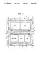
- FIG. 1 is a chip layout showing the fundamental structure of a semiconductor integrated circuit device having a system including a microprocessor unit according to the embodiment I of the present invention
- FIG. 2 is a diagram showing the equivalent circuits of the interface circuits of said semiconductor integrated circuit device of the present invention
- FIG. 3 is a schematic block diagram showing said semiconductor integrated circuit device of the present invention mounted on a printed circuit board
- FIG. 4 is a chip layout showing the fundamental structure of a semiconductor integrated circuit device having a system including a microprocessor unit according to the embodiment II of the present invention.
- the present invention is applied to a semiconductor integrated circuit device using a standard cell method of a custom ASIC, the structure of the present invention will subsequently be described.
- FIG. 1 The fundamental structure of a semiconductor integrated circuit device using the standard cell method with a system including a microprocessing module according to the embodiment I of the present invention is shown in FIG. 1 (a chip layout).
- the semiconductor integrated circuit device 1 is a rectangular chip in its plan (for example, a monolithic silicon substrate).
- This semiconductor integrated circuit device 1 is formed by the standard cell method of a custom type, although it is not limited to such a method.
- a logic system including a microprocessor unit (MPU) 5 is mounted on the central portion of the rectangular semiconductor integrated circuit device 1.
- Said logic system is made up, though not limited to, such units as a direct memory access controller unit (DMAC) 6, a memory unit (ROM/RAM) 7, a hard disk controller unit (HDC) 8 and a floppy disk controller unit (FDC) 9 in addition to the microprocessor unit 5.
- DMAC direct memory access controller unit
- ROM/RAM memory unit
- HDC hard disk controller unit
- FDC floppy disk controller unit
- Each of these units 5 to 9 comprising the logic system is respectively a unit of module representing one functional block or circuit block.
- Each of these units 5 to 9 is automatically arranged on the semiconductor substrate as a macro cell in the automatic wiring distribution system (DA).
- DA automatic wiring distribution system
- the memory unit 7 is formed by such a RAM as either a DRAM or an SRAM, or both and also formed by such a ROM as either one of a mask, ROM, an EPROM, an EEPROM or a combination of these ROM's.
- the microprocessor unit 5 and the direct memory access controller unit 6 of said logic system are arranged on the upper side of the main surface of the semiconductor substrate of the semiconductor integrated circuit device 1, and the memory unit 7, the hard disk controller unit 8 and the floppy disk controller unit 9 of said logic system are arranged on the lower side of the main surface of the semiconductor substrate of the semiconductor integrated circuit device 1.
- Each of these units 5 to 9 of said logic system is made up with circuits formed mainly by CMOS for the fundamental purpose of a higher integration thereof.
- the respectivecircuits of said units 5 to 9 for which a driving capacity is required, such as their output circuits, are formed by bipolar transistors or by compound circuits made up with bipolar transistor and CMOS.
- the semiconductor integrated circuit device 1 of this embodiment is formed by the so-called Bi-CMOS which allows bipolar transistor and CMOS to coexist with each other on the main surface of the same and one semiconductor substrate.
- a plurality of interface circuits (input/output buffering circuits) 3 are arranged, and further along the outer circumference of the interface circuits 3 of the semiconductor integrated circuit device 1, a plurality of the external terminals (bonding pads) 2, 2A are arranged respectively.
- the external terminals 2 are used as the ones for the input or output signals for connecting each of the units 5 to 9 of the logic system of the semiconductor integrated circuit device 1 and the external device arranged outside the semiconductor integrated circuit device 1.
- the external terminals 2 are each arranged in almost all the circumferential region of said logic system.
- the external terminals 2A connect, as shown in FIG. 3 (a schematic block diagram showing the state when mounted on a printed board), each of the common internal bus lines (common signal wirings) 4 arranged within the semiconductor integrated circuit device 1 and the common external bus line 11 arranged outside the semiconductor integrated circuit device 1.
- the external bus line 2A is used as the one dedicated only for the input or output signals for the bus line.
- a plurality of the external terminals 2A are arranged each on the central portions of the two opposite sides of a rectangular chip of the semiconductor integrated circuit device 1 of this embodiment.
- the common internal bus line 4 connected to said external terminals 2A used only for the bus line is arranged on the central portion of the semiconductor integrated circuit device 1. Specifically, the common internal bus line 4 is arranged between the units 5 and 6 located at the upper side of the semiconductor integrated circuit device 1 and the units 7 to 9 located at the lower side thereof. In other words, this common internal bus line 4 extends across from one side of the opposite two sides of the rectangular chip to the other side (in the transverse direction in FIG. 1).
- the common internal bus line 4 constitutes signal wirings common to each of the units 5 to 9 of said logic system.
- the common internal bus line 4 is made up with a plurality of signal wirings extending substantially in parallel in the same and one direction with a given wiring pitch.
- the common internal bus line 4 is formed as an integrated body having approximately several tens to several hundreds of wirings which transfer common signals in such systems as clock, data, addressing and controlling.
- the common internal bus line 4 is formed in either one of the wiring layers of the double-layer wiring structure.
- the common external bus line 11 is not shown in FIG. 1, it is arranged on a printed circuit board on which, for example, the semiconductor integrated circuit device 1 is mounted. On the printed circuit board, the external device 10 having a floppy disk controller (FDC) and others are mounted as shown in FIG. 3. The external device 10 and the semiconductor integrated circuit device 1 are respectively connected with each other through the common external bus line 11 as previously described.
- the common external bus line 11 is made up with approximately the same number of signal wirings as said common internal bus line 4.
- a plurality of said interface circuits 3 are respectively arranged between the units 5 to 9 of said logic system and the external terminals 2.
- the interface circuits 3 are formed as interface circuits connecting said units 5 to 9 and the respectively external devices.
- the interface circuits 3 are formed by, for example, three-state buffering circuits as shown in FIG. 2 (an equivalent circuit diagram).
- the interface circuits 3 shown in FIG. 2 are made up mainly with CMOS, bipolar transistors, resistance elements and Schottky barrier diode elements.
- the interface circuits 3 are formed in a totem pole structure having bipolar transistors at their output stage for intensifying driving capacity when they are provided for the output use.
- FIG. 2 an equivalent circuit diagram
- the interface circuits 3 are formed by connecting each semiconductor element for the interface circuit cells arranged in advance on a semiconductor substrate by a fundamental design on each of said semiconductor elements with the wirings provided in the first layer of the wiring layer of said double-layer wiring structure.
- a plurality of interface circuits 3A are arranged between each of the units 5 to 9 of said logic system and the common internal bus line 4 are connected with each other.
- the interface circuits 3A have almost the same structure as the interface circuits 3 except that several CMOS's arranged in the vicinity of the input signal terminal IN shown in FIG. 2 (CMOS's in the region surrounded by dotted lines) are not provided.
- the interface circuits 3A are formed in a smaller area than the interface circuits 3 by the size equivalent to the area occupied by said several CMOS's.
- the interface circuits 3A are formed by connecting each semiconductor element for interface circuit cells with the wiring layer of the first layer as in the case of said interface circuits 3.
- each of the units 5 and 6 of the logic system is connected to the external terminals 2A through the interface circuits 3A, and each of said external terminals 2A and interface circuits 3A is connected with each other through the common internal bus line 4 provided between each of said units 5 to 9.
- each of the units 5 to 9 of the logic system of the semiconductor integrated circuit device 1 and the common external bus line 11 is connected from the side of each of said units 5 to 9 sequentially through the interface circuits 3A, the common internal bus line 4 and the external terminals 2A respectively.
- This structure makes it unnecessary to arrange the interface circuits 3A and the external terminals 2A each in response to the number of the respective signal wirings of the common external bus line 11 for each of the units 5 to 9 of said logic system. It suffices if only the interface circuits 3A and the external terminals 2A are arranged each in the number corresponding to the number of the respective wirings of said common internal bus line 4. Thus, the required numbers in which the interface circuits 3A and the external terminals 2A can be reduced so as to improve the mounting efficiency of the units. In other words, the integration of the semiconductor integrated circuit device 1 can be improved.
- said common internal bus line 4 is arranged in the central portion of said semiconductor substrate, and each of the units 5 to 9 of said logic system is arranged on the main surface of the semiconductor substrate along both sides of the common internal bus line 4.
- the wiring length of said common internal bus line 4 is minimized so that the accidental capacity or loaded resistance on the common internal bus line 4 can be reduced.
- the transfer speed of the signals in the common internal bus line 4 is made faster so that the operation of the logic system can carried out at a higher speed. In other words, the operational speed of the semiconductor integrated circuit device 1 can be made faster.
- the interface circuits 3A connected to said common internal bus line 4 are formed in a smaller area than the area occupied by the interface circuits 3 connected to signal wirings other than those of said common internal bus line 4.
- the area occupied only by the interface circuits 3A connected to said common internal bus line 4 can be reduced so as to improve the mounting efficiency of said units.
- the interface circuits 3A connected to said common internal bus line 4 are formed by bipolar transistors at least at their output stage.
- the driving capacity of the interface circuits 3A connected to said common internal bus line 4 is more intensified than it is formed by CMOS.
- the external device 10 can be driven directly only by said interface circuits 3A.
- there is no need of outside devices dedicated for intensifying the driving capacity so that the mounting density of a printed circuit board can be improved.
- the number of parts is reduced so that the mounting efficiency can be improved.
- the bipolar transistor has a higher resistance against electrostatic breakage than CMOS transistors have, each of the interface circuits 3A and 3 is protected against electrostatic breakage.
- the common internal bus line 4 is provided in said semiconductor integrated circuit device 1.
- the common internal bus line 4 is automatically arranged by the automatic wiring distribution system, it is arranged in a fixed pattern such as power wirings separately from those signal wirings connecting each of units 5 to 9 or logic circuits arranged within each of the units 5 to 9.
- the wiring loads on the respective signal wirings of the common internal bus line 4 can be equalized.
- each of the units 5 to 9 is made up mainly with CMOS, skew is prevented.
- the operation of said logic system can be carried out at a higher speed because, although CMOS depends more on the wiring load for its operational speed, it allows the wiring load of the common internal bus line 4 to be equalized.
- the embodiment II is the second embodiment of the present invention wherein the common internal bus line is arranged in the circumference of said logic system in the semiconductor integrated circuit device using the standard cell method described in said embodiment I.
- FIG. 4 The fundamental structure of the semiconductor integrated circuit device using the standard cell method having a system including a microprocessor unit which is the second embodiment of the present invention is shown in FIG. 4 (a chip layout).
- the semiconductor integrated circuit device 1 of the embodiment II has the common internal bus line 4 arranged in the circumference of the logic system formed by the microprocessor unit 5 and others.
- the common internal bus line 4 is arranged between the interface circuits 3 and 3A and the external terminals 2 and 2A (or may be arranged around the external terminals 2), so that it surrounds said logic system in a ring.
- a plurality of interface circuits 3 are arranged between said logic system and internal bus line 4.
- the interface circuits 3A dedicated only for the bus line provided between each of the units 5 to 9 and the common internal bus line 4 is arranged regularly or at random along the array of the interface circuits 3 in the region in which the interface circuits 3 are arranged.
- such external terminal 2 as arranged in a given region such as the vicinity of the interface circuit 3A is connected to the common internal bus line 4 in the process of wiring formation and is used as the external terminal 2A dedicated only for bus line.
- the common internal bus line 4 is arranged on the main surface of a semiconductor substrate along the out circumference of said logic system in the semiconductor integrated circuit device 1 using said standard cell method.
- the mounting efficiency of said logic system can be improved to the extent corresponding to the area that would be occupied by said common internal bus line 4 because said common internal bus line 4 can be arranged in a space substantially independent of the region in which said logic system is mounted (the region where each of the units 5 to 9 is arranged).
- each of the units 5 to 9 of said logic system is in a region substantially independent of said common internal bus line 4 so that the arrangement of the units 5 to 9 is not restricted by that of the common internal bus line 4.
- each of the units 5 to 9 of the logic system can be arranged more flexibly.
- the interface circuits 3A connected to said common internal bus line 4 are arranged in the region in which the interface circuits 3 connected to the signal wirings other than those of said common internal bus line 4 is arranged. In other words, the interface circuits 3A connected to the common internal bus line 4 are arranged along the array of the interface circuits 3 connected to the signal wiring.
- the units 5 to 9 of semiconductor integrated circuit device 1 can be arranged more flexibly.
- the present invention is respectively applicable to a semiconductor integrated circuit device using the full custom type of a custom method and a semiconductor integrated circuit device using the semi custom type of a gate array method.
- the present invention is applicable to a semiconductor integrated circuit device having a multiple-layer wiring structure such as three layers or more.
- the mounting efficiency of circuits can be improved.
- the operation of the system can be carried out at a higher speed.
- the driving capacity of external devices can be intensified.
- the semiconductor integrated circuit device having a system including a microprocessing module, while the mounting efficiency of the circuits can be improved, the driving capacity of external devices can be intensified.
- the mounting device on the circuit board of which said semiconductor integrated circuit device is mounted, the mounting device can be improved.
Landscapes
- Engineering & Computer Science (AREA)
- Microelectronics & Electronic Packaging (AREA)
- Semiconductor Integrated Circuits (AREA)
- Design And Manufacture Of Integrated Circuits (AREA)
- Microcomputers (AREA)
Applications Claiming Priority (2)
| Application Number | Priority Date | Filing Date | Title |
|---|---|---|---|
| JP1-40528 | 1989-02-20 | ||
| JP1040528A JPH02219254A (ja) | 1989-02-20 | 1989-02-20 | 半導体集積回路装置 |
Publications (1)
| Publication Number | Publication Date |
|---|---|
| US5017993A true US5017993A (en) | 1991-05-21 |
Family
ID=12582975
Family Applications (1)
| Application Number | Title | Priority Date | Filing Date |
|---|---|---|---|
| US07/482,077 Expired - Fee Related US5017993A (en) | 1989-02-20 | 1990-02-20 | Semiconductor integrated circuit device with bus lines |
Country Status (3)
| Country | Link |
|---|---|
| US (1) | US5017993A (ja) |
| JP (1) | JPH02219254A (ja) |
| KR (1) | KR900013622A (ja) |
Cited By (11)
| Publication number | Priority date | Publication date | Assignee | Title |
|---|---|---|---|---|
| US5319224A (en) * | 1989-10-11 | 1994-06-07 | Mitsubishi Denki Kabushiki Kaisha | Integrated circuit device having a geometry to enhance fabrication and testing and manufacturing method thereof |
| US5369777A (en) * | 1990-08-31 | 1994-11-29 | Advanced Micro Devices, Inc. | Integrated digital processing apparatus having a single biodirectional data bus for accommodating a plurality of peripheral devices connected to a plurality of external buses |
| US5424248A (en) * | 1991-12-10 | 1995-06-13 | Vlsi Technology, Inc. | Method of making an integrated circuit with variable pad pitch |
| US5468992A (en) * | 1991-02-28 | 1995-11-21 | Hitachi, Ltd. | Electronic circuit package including plural bare chips mounted on a single wiring substrate |
| US5495422A (en) * | 1993-10-12 | 1996-02-27 | Wang Laboratories, Inc. | Method for combining a plurality of independently operating circuits within a single package |
| US5509019A (en) * | 1990-09-20 | 1996-04-16 | Fujitsu Limited | Semiconductor integrated circuit device having test control circuit in input/output area |
| EP0725349A3 (en) * | 1995-01-31 | 1997-07-09 | Mitsubishi Electric Corp | Microcomputer chip arrangement |
| US5915103A (en) * | 1996-12-05 | 1999-06-22 | Vlsi Technology, Inc. | Method and system for an extensible on silicon bus supporting multiple functional blocks |
| US6073200A (en) * | 1998-01-27 | 2000-06-06 | Vlsi Technology, Inc. | System having processor monitoring capability of an integrated circuits buried, internal bus for use with a plurality of internal masters and a method therefor |
| US6979908B1 (en) * | 2000-01-11 | 2005-12-27 | Texas Instruments Incorporated | Input/output architecture for integrated circuits with efficient positioning of integrated circuit elements |
| US20080111211A1 (en) * | 2006-11-13 | 2008-05-15 | Nair Pratheep A | On-chip capacitors for addressing power supply voltage drops |
Families Citing this family (3)
| Publication number | Priority date | Publication date | Assignee | Title |
|---|---|---|---|---|
| JP3006810B2 (ja) * | 1992-05-27 | 2000-02-07 | 日本電気株式会社 | 半導体集積回路 |
| WO1998025213A1 (en) * | 1996-12-04 | 1998-06-11 | Hitachi, Ltd. | Semiconductor integrated circuit device |
| JP2004134599A (ja) * | 2002-10-11 | 2004-04-30 | Renesas Technology Corp | 半導体装置、およびそのレイアウト方法 |
Citations (4)
| Publication number | Priority date | Publication date | Assignee | Title |
|---|---|---|---|---|
| JPS6076141A (ja) * | 1983-10-03 | 1985-04-30 | Nec Corp | 集積論理回路 |
| JPS63285945A (ja) * | 1987-05-18 | 1988-11-22 | Fujitsu Ltd | 半導体集積回路及び製造方法 |
| JPS63310134A (ja) * | 1987-06-12 | 1988-12-19 | Fujitsu Ltd | 半導体集積回路装置 |
| JPS6414055A (en) * | 1987-07-09 | 1989-01-18 | Canon Kk | Thermal recording method |
-
1989
- 1989-02-20 JP JP1040528A patent/JPH02219254A/ja active Pending
-
1990
- 1990-02-15 KR KR1019900001837A patent/KR900013622A/ko not_active Withdrawn
- 1990-02-20 US US07/482,077 patent/US5017993A/en not_active Expired - Fee Related
Patent Citations (4)
| Publication number | Priority date | Publication date | Assignee | Title |
|---|---|---|---|---|
| JPS6076141A (ja) * | 1983-10-03 | 1985-04-30 | Nec Corp | 集積論理回路 |
| JPS63285945A (ja) * | 1987-05-18 | 1988-11-22 | Fujitsu Ltd | 半導体集積回路及び製造方法 |
| JPS63310134A (ja) * | 1987-06-12 | 1988-12-19 | Fujitsu Ltd | 半導体集積回路装置 |
| JPS6414055A (en) * | 1987-07-09 | 1989-01-18 | Canon Kk | Thermal recording method |
Non-Patent Citations (2)
| Title |
|---|
| Denshi Zairyo (Elect. Matls) Jul. 87, pp. 49 52, Kogyo Chosakai, Co., Inc. * |
| Denshi Zairyo (Elect. Matls) Jul. 87, pp. 49-52, Kogyo Chosakai, Co., Inc. |
Cited By (26)
| Publication number | Priority date | Publication date | Assignee | Title |
|---|---|---|---|---|
| US5319224A (en) * | 1989-10-11 | 1994-06-07 | Mitsubishi Denki Kabushiki Kaisha | Integrated circuit device having a geometry to enhance fabrication and testing and manufacturing method thereof |
| US5369777A (en) * | 1990-08-31 | 1994-11-29 | Advanced Micro Devices, Inc. | Integrated digital processing apparatus having a single biodirectional data bus for accommodating a plurality of peripheral devices connected to a plurality of external buses |
| US5509019A (en) * | 1990-09-20 | 1996-04-16 | Fujitsu Limited | Semiconductor integrated circuit device having test control circuit in input/output area |
| US6584004B2 (en) | 1991-02-28 | 2003-06-24 | Hitachi, Ltd. | Electronic circuit package |
| US6728904B2 (en) | 1991-02-28 | 2004-04-27 | Hitachi, Ltd. | Electronic circuit package |
| US5468992A (en) * | 1991-02-28 | 1995-11-21 | Hitachi, Ltd. | Electronic circuit package including plural bare chips mounted on a single wiring substrate |
| US20070158814A1 (en) * | 1991-02-28 | 2007-07-12 | Nobuyasu Kanekawa | Electronic circuit package |
| US5614761A (en) * | 1991-02-28 | 1997-03-25 | Hitachi, Ltd. | Electronic circuit package including plural semiconductor chips formed on a wiring substrate |
| US7233534B2 (en) | 1991-02-28 | 2007-06-19 | Hitachi, Ltd. | Electronic circuit package |
| US7120069B2 (en) | 1991-02-28 | 2006-10-10 | Hitachi, Ltd. | Electronic circuit package |
| US20080303175A1 (en) * | 1991-02-28 | 2008-12-11 | Nobuyasu Kanekawa | Electronic circuit package |
| US5789805A (en) * | 1991-02-28 | 1998-08-04 | Hitachi, Ltd. | Semiconductor multi-chip module |
| US20040164324A1 (en) * | 1991-02-28 | 2004-08-26 | Nobuyasu Kanekawa | Electronic circuit package |
| US7701743B2 (en) | 1991-02-28 | 2010-04-20 | Rising Silicon, Inc. | Electronic circuit package |
| US6223273B1 (en) | 1991-02-28 | 2001-04-24 | Hitachi, Ltd. | Electronic circuit package |
| US7425763B2 (en) | 1991-02-28 | 2008-09-16 | Hitachi, Ltd. | Electronic circuit package |
| US5424248A (en) * | 1991-12-10 | 1995-06-13 | Vlsi Technology, Inc. | Method of making an integrated circuit with variable pad pitch |
| US5742079A (en) * | 1991-12-10 | 1998-04-21 | Vlsi Technology, Inc. | Integrated circuit with variable pad pitch |
| US5610417A (en) * | 1991-12-10 | 1997-03-11 | Vlsi Technology, Inc. | Integrated circuit with variable pad pitch |
| US5495422A (en) * | 1993-10-12 | 1996-02-27 | Wang Laboratories, Inc. | Method for combining a plurality of independently operating circuits within a single package |
| US5787310A (en) * | 1995-01-31 | 1998-07-28 | Mitsubishi Denki Kabushiki Kaisha | Microcomputer |
| EP0725349A3 (en) * | 1995-01-31 | 1997-07-09 | Mitsubishi Electric Corp | Microcomputer chip arrangement |
| US5915103A (en) * | 1996-12-05 | 1999-06-22 | Vlsi Technology, Inc. | Method and system for an extensible on silicon bus supporting multiple functional blocks |
| US6073200A (en) * | 1998-01-27 | 2000-06-06 | Vlsi Technology, Inc. | System having processor monitoring capability of an integrated circuits buried, internal bus for use with a plurality of internal masters and a method therefor |
| US6979908B1 (en) * | 2000-01-11 | 2005-12-27 | Texas Instruments Incorporated | Input/output architecture for integrated circuits with efficient positioning of integrated circuit elements |
| US20080111211A1 (en) * | 2006-11-13 | 2008-05-15 | Nair Pratheep A | On-chip capacitors for addressing power supply voltage drops |
Also Published As
| Publication number | Publication date |
|---|---|
| JPH02219254A (ja) | 1990-08-31 |
| KR900013622A (ko) | 1990-09-06 |
Similar Documents
| Publication | Publication Date | Title |
|---|---|---|
| US5172330A (en) | Clock buffers arranged in a peripheral region of the logic circuit area | |
| JPH05308136A (ja) | マスタスライス集積回路 | |
| US4947233A (en) | Semi-custom LSI having input/output cells | |
| US5258891A (en) | Multichip module with multilayer wiring substrate | |
| US5641978A (en) | Input/output buffer layout having overlapping buffers for reducing die area of pad-limited integrated circuit | |
| KR100447066B1 (ko) | 멀티 칩 모듈 | |
| JPH07263628A (ja) | 半導体装置 | |
| JPH02219254A (ja) | 半導体集積回路装置 | |
| US5742079A (en) | Integrated circuit with variable pad pitch | |
| US6979908B1 (en) | Input/output architecture for integrated circuits with efficient positioning of integrated circuit elements | |
| KR100404487B1 (ko) | 반도체 집적 회로 | |
| US5206529A (en) | Semiconductor integrated circuit device | |
| JPH0120536B2 (ja) | ||
| US6172547B1 (en) | Semiconductor integrated circuit capable of driving large loads within its internal core area | |
| KR19990088410A (ko) | 반도체장치 | |
| JPH0542823B2 (ja) | ||
| JPH03201551A (ja) | 半導体集積回路装置 | |
| JP3186715B2 (ja) | 半導体集積回路装置 | |
| JPH06101521B2 (ja) | 半導体集積回路装置 | |
| JPS61225845A (ja) | 半導体装置 | |
| JPH03203363A (ja) | 半導体装置 | |
| JPH09153286A (ja) | 半導体記憶装置 | |
| JPH01152642A (ja) | 半導体集積回路 | |
| JPS6380622A (ja) | 半導体集積回路装置 | |
| JPH0210582B2 (ja) |
Legal Events
| Date | Code | Title | Description |
|---|---|---|---|
| AS | Assignment |
Owner name: HITACHI, LTD., TOKYO 101, JAPAN Free format text: ASSIGNMENT OF ASSIGNORS INTEREST.;ASSIGNOR:SHIBATA, MANABU;REEL/FRAME:005544/0147 Effective date: 19900209 |
|
| FEPP | Fee payment procedure |
Free format text: PAYOR NUMBER ASSIGNED (ORIGINAL EVENT CODE: ASPN); ENTITY STATUS OF PATENT OWNER: LARGE ENTITY |
|
| FPAY | Fee payment |
Year of fee payment: 4 |
|
| FPAY | Fee payment |
Year of fee payment: 8 |
|
| REMI | Maintenance fee reminder mailed | ||
| LAPS | Lapse for failure to pay maintenance fees | ||
| STCH | Information on status: patent discontinuation |
Free format text: PATENT EXPIRED DUE TO NONPAYMENT OF MAINTENANCE FEES UNDER 37 CFR 1.362 |
|
| FP | Lapsed due to failure to pay maintenance fee |
Effective date: 20030521 |