US5160984A - Amplifying feedback FET semiconductor element - Google Patents
Amplifying feedback FET semiconductor element Download PDFInfo
- Publication number
- US5160984A US5160984A US07/732,934 US73293491A US5160984A US 5160984 A US5160984 A US 5160984A US 73293491 A US73293491 A US 73293491A US 5160984 A US5160984 A US 5160984A
- Authority
- US
- United States
- Prior art keywords
- fet
- lead electrode
- transistor elements
- drain
- feedback
- Prior art date
- Legal status (The legal status is an assumption and is not a legal conclusion. Google has not performed a legal analysis and makes no representation as to the accuracy of the status listed.)
- Expired - Fee Related
Links
Images



Classifications
-
- H—ELECTRICITY
- H03—ELECTRONIC CIRCUITRY
- H03F—AMPLIFIERS
- H03F3/00—Amplifiers with only discharge tubes or only semiconductor devices as amplifying elements
- H03F3/189—High-frequency amplifiers, e.g. radio frequency amplifiers
- H03F3/19—High-frequency amplifiers, e.g. radio frequency amplifiers with semiconductor devices only
- H03F3/193—High-frequency amplifiers, e.g. radio frequency amplifiers with semiconductor devices only with field-effect devices
-
- H—ELECTRICITY
- H03—ELECTRONIC CIRCUITRY
- H03F—AMPLIFIERS
- H03F1/00—Details of amplifiers with only discharge tubes, only semiconductor devices or only unspecified devices as amplifying elements
- H03F1/34—Negative-feedback-circuit arrangements with or without positive feedback
-
- H—ELECTRICITY
- H03—ELECTRONIC CIRCUITRY
- H03F—AMPLIFIERS
- H03F3/00—Amplifiers with only discharge tubes or only semiconductor devices as amplifying elements
- H03F3/60—Amplifiers in which coupling networks have distributed constants, e.g. with waveguide resonators
- H03F3/602—Combinations of several amplifiers
- H03F3/604—Combinations of several amplifiers using FET's
-
- H—ELECTRICITY
- H03—ELECTRONIC CIRCUITRY
- H03F—AMPLIFIERS
- H03F2200/00—Indexing scheme relating to amplifiers
- H03F2200/372—Noise reduction and elimination in amplifier
Definitions
- This invention relates to an amplifying FET (Field Effect Transistor) semiconductor element equipped with a feedback circuit for a monolithic IC. More particularly the invention relates to an amplifying feedback-type FET semiconductor element having a wide-band frequency characteristic and adapted to be used in communications systems such as radar.
- FET Field Effect Transistor
- GaAs FETs are widely used as semiconductor elements for microwave amplifiers which are low-noise and high-gain.
- this kind of wide-band amplifier using FETs has been further developed into a GaAs monolithic IC form.
- resistors can be easily produced from GaAs
- a wide-band amplifier can be accomplished by providing the GaAs FET with a negative feedback by the resistor.
- FIG. 5 of the accompanying drawings is a circuit diagram showing a typical conventional feedback-type field-effect-transistor amplifier (hereinafter called “feedback-type FET amplifier”) disclosed in a thesis publication MW80-80 entitled “GaAs Monolithic IC Ultrawide-band Low-noise Amplifier” (by Nishiuma et al.) issued from The Institute of Electronics, Information and Communication Engineers.
- feedback-type FET amplifier a typical conventional feedback-type field-effect-transistor amplifier
- FIG. 5 designates a field effect transistor (hereinafter called "FET") which has a gate terminal 2, a drain terminal 3 and a source terminal 4.
- the source terminal 4 is connected to the ground.
- the gate and drain terminals 2, 3 of the FET 1 are connected by a feedback circuit 8 composed of a resistor 5, a capacitor 6 and connecting transmission lines 7.
- this feedback circuit 8 includes passive elements, i.e. the resistor 5 and the capacitor 6, and the connecting transmission lines 7.
- the impedance Z f of the feed-back circuit 8 is expressed by the following equation:
- R f is the value of the resistor 5
- C f is the value of the capacitor 6
- L f is the value of the inductance of the connecting transmission lines 7.
- this amplifier can have good input and output reflection characteristics over a wide frequency band and also a frequency characteristic showing a flat gain over a wide frequency band.
- FIG. 6 is a chip pattern diagram showing one example of the conventional amplifying feedback-type FET semiconductor element of FIG. 5.
- an amplifying feedback-type FET semiconductor element comprising: an FET transistor element including a plurality of parallel FET cells each composed of a semiconductor substrate, and source, drain and gate electrodes mounted on the substrate; a drain lead electrode extending from the drain electrode of each of the FET cells and disposed on substrate at one side of the FET semiconductor element; a gate lead electrode extending from the gate electrode of each of the FET cells and disposed on the substrate at the other side of the FET semiconductor element; and a feedback circuit including at least two connecting lines and at least one passive element and being connected to the drain lead electrode and the gate lead electrode, the feedback circuit being located between the drain and gate lead electrodes and also between the FET cells so as to reduce the total length of the connecting lines to a minimum.
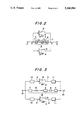
- FIG. 1 is a chip pattern diagram showing an amplifying feedback-type FET semiconductor element of this invention
- FIG. 2 is a circuit diagram showing a first embodiment of the feedback-type FET semiconductor element of FIG. 1;
- FIG. 3 is a circuit diagram showing a second embodiment in which the feedback-type FET semiconductor element is equipped with input and output circuits;
- FIG. 4 is a circuit diagram showing a third embodiment in which the feedback-type FET semiconductor element includes three parallel FET cells;
- FIG. 5 is a circuit diagram showing a conventional amplifying feedback-type FET semiconductor element.
- FIG. 6 is a chip pattern diagram showing the conventional feedback-type FET semiconductor element of FIG. 5.
- FIGS. 1 and 2 show an amplifying feedback-type FET semiconductor element according to a first embodiment of this invention. This feedback-type FET semiconductor element is particularly useful when used as an amplifier.
- the amplifier generally comprises a gate terminal 2, a drain terminal 3, a feedback circuit 8 connected to the gate and drain terminals 2, 3, and two FET cells 9. All of these components are mounted on a semiconductor substrate.
- Each of the FET cells 9 is composed of source, drain and gate electrodes.
- the gate terminal 2 is a gate lead electrode disposed on the substrate and extends from the gate electrode.
- the drain terminal 3 is a drain lead electrode disposed on the substrate and extends from the gate electrode.
- the feedback circuit 8 is connected in series to said gate and drain terminals 2, 3 and is located between the two FET cells 9, 9.
- the feedback circuit 8 is composed of connecting transmission lines 7, and passive elements, i.e. a capacitor 6 and a resistor 5.
- Each of the gate and drain terminals 2, 3, as shown in FIG. 1, has a comb-shaped contour.
- the gate terminal 2 and the drain terminal 3 are disposed in confronting relationship. Between the two terminals 2, 3 is disposed, the source terminals 4 and the feedback circuit 8.
- FIG. 2 shows an equivalent circuit corresponding to the chip pattern diagram of FIG. 1.
- the two FET cells 9, 9 are connected in parallel.
- This amplifier is constituted by connecting the feedback circuit 8 in parallel to the two FET cells 9, i.e. FET semiconductor elements.
- the feedback circuit 8 is located between the two FET cells 9, 9 and is connected at one end to the drain terminal 3, i.e. the drain lead electrode, and at the other end to the gate terminal 2, i.e. the gate lead electrode.
- the feedback circuit 8 is composed of the resistor 5, the capacitor 6 and the connecting transmission lines 7, which components are all connected in series.
- the FET semiconductor element as shown in FIG. 1, is divided into two parallel FET cells 9, 9, the feedback circuit 8 of this amplifier can be located between these two FET cells 9, 9 so that the feedback circuit 8 can be formed on the shortest path between the gate and drain terminals 2, 3.
- the total length of the connecting transmission lines 7 of the feedback circuit 8 is reduced to a minimum. Because of this sufficiently short length of the connecting lines 7, the inductance L f can be almost neglected.
- FIG. 3 shows an amplifying feedback-type FET semiconductor element according to a second embodiment.
- This feedback-type FET semiconductor element comprises the feedback circuit 8 and two FET cells 9, 9, each including input and output side circuits 10, 11. These two FET cells 9, 9 and the feedback circuit 8 are connected in parallel to one another.
- the feedback circuit 8 is connected between the input terminal 12 to, which the input side circuit 10 is added to the gate terminals of the FET cells 9, and the output terminal 13 to, which the output side circuit 11 is added to the drain terminals of the FET cells 9.
- FIG. 4 shows a third embodiment, in which a multiplicity of FET cells 9 (three FET cells in this embodiment) are connected in parallel and in which a plurality of feedback circuits 8 (two feedback circuits in this embodiment) are located one between each adjacent two of the FET cells 9, 9.
- the amplifying feedback-type FET semiconductor element since at least one feedback circuit is located between two or more FET cells and between the drain lead electrode and the gate lead electrode, it is possible to reduce the total length of connecting transmission lines to a minimum even if the amplifying FET semiconductor element having a large gate width is equipped with the feedback circuit, thus guaranteeing a frequency characteristic showing a flat gain over a wide frequency band.
Landscapes
- Engineering & Computer Science (AREA)
- Power Engineering (AREA)
- Amplifiers (AREA)
Applications Claiming Priority (2)
| Application Number | Priority Date | Filing Date | Title |
|---|---|---|---|
| JP1-66901 | 1989-03-17 | ||
| JP1066901A JP2555726B2 (ja) | 1989-03-17 | 1989-03-17 | 帰還形電界効果トランジスタ増幅器 |
Related Parent Applications (1)
| Application Number | Title | Priority Date | Filing Date |
|---|---|---|---|
| US07485171 Continuation | 1990-02-26 |
Publications (1)
| Publication Number | Publication Date |
|---|---|
| US5160984A true US5160984A (en) | 1992-11-03 |
Family
ID=13329306
Family Applications (1)
| Application Number | Title | Priority Date | Filing Date |
|---|---|---|---|
| US07/732,934 Expired - Fee Related US5160984A (en) | 1989-03-17 | 1991-07-19 | Amplifying feedback FET semiconductor element |
Country Status (4)
| Country | Link |
|---|---|
| US (1) | US5160984A (ja) |
| JP (1) | JP2555726B2 (ja) |
| FR (1) | FR2644648B1 (ja) |
| GB (1) | GB2230396B (ja) |
Cited By (5)
| Publication number | Priority date | Publication date | Assignee | Title |
|---|---|---|---|---|
| US5283452A (en) * | 1992-02-14 | 1994-02-01 | Hughes Aircraft Company | Distributed cell monolithic mircowave integrated circuit (MMIC) field-effect transistor (FET) amplifier |
| US6081006A (en) * | 1998-08-13 | 2000-06-27 | Cisco Systems, Inc. | Reduced size field effect transistor |
| US6642578B1 (en) | 2002-07-22 | 2003-11-04 | Anadigics, Inc. | Linearity radio frequency switch with low control voltage |
| US6730945B2 (en) * | 2001-09-26 | 2004-05-04 | Mitsubishi Denki Kabushiki Kaisha | Semiconductor device |
| CN113874996A (zh) * | 2019-05-27 | 2021-12-31 | 住友电工光电子器件创新株式会社 | 放大装置 |
Citations (6)
| Publication number | Priority date | Publication date | Assignee | Title |
|---|---|---|---|---|
| JPS5892272A (ja) * | 1981-11-27 | 1983-06-01 | Mitsubishi Electric Corp | 負帰還型GaAsマイクロ波モノリシツク増幅回路装置 |
| JPS5892271A (ja) * | 1981-11-27 | 1983-06-01 | Mitsubishi Electric Corp | GaAsマイクロ波モノリシツク集積回路装置 |
| JPS60237709A (ja) * | 1984-05-11 | 1985-11-26 | Mitsubishi Electric Corp | モノリシツクマイクロ波増幅器 |
| JPS62159907A (ja) * | 1986-01-08 | 1987-07-15 | Mitsubishi Electric Corp | モノリシツクマイクロ波増幅器 |
| US4760350A (en) * | 1987-06-08 | 1988-07-26 | Hittite Microwave Corporation | Internally matched power amplifier |
| US4786881A (en) * | 1987-08-27 | 1988-11-22 | General Electric Company | Amplifier with integrated feedback network |
Family Cites Families (4)
| Publication number | Priority date | Publication date | Assignee | Title |
|---|---|---|---|---|
| US3596203A (en) * | 1968-01-04 | 1971-07-27 | Nippon Electric Co | Plural transistor high frequency oscillator |
| JPS5724569A (en) * | 1980-07-18 | 1982-02-09 | Mitsubishi Electric Corp | Uhf band gaas fet |
| FR2533777B1 (fr) * | 1982-09-24 | 1987-09-04 | Thomson Csf | Oscillateur hyperfrequence de puissance |
| JPS60140907A (ja) * | 1983-12-28 | 1985-07-25 | Matsushita Electric Ind Co Ltd | 半導体集積回路 |
-
1989
- 1989-03-17 JP JP1066901A patent/JP2555726B2/ja not_active Expired - Lifetime
-
1990
- 1990-03-14 GB GB9005758A patent/GB2230396B/en not_active Expired - Fee Related
- 1990-03-16 FR FR9003415A patent/FR2644648B1/fr not_active Expired - Fee Related
-
1991
- 1991-07-19 US US07/732,934 patent/US5160984A/en not_active Expired - Fee Related
Patent Citations (6)
| Publication number | Priority date | Publication date | Assignee | Title |
|---|---|---|---|---|
| JPS5892272A (ja) * | 1981-11-27 | 1983-06-01 | Mitsubishi Electric Corp | 負帰還型GaAsマイクロ波モノリシツク増幅回路装置 |
| JPS5892271A (ja) * | 1981-11-27 | 1983-06-01 | Mitsubishi Electric Corp | GaAsマイクロ波モノリシツク集積回路装置 |
| JPS60237709A (ja) * | 1984-05-11 | 1985-11-26 | Mitsubishi Electric Corp | モノリシツクマイクロ波増幅器 |
| JPS62159907A (ja) * | 1986-01-08 | 1987-07-15 | Mitsubishi Electric Corp | モノリシツクマイクロ波増幅器 |
| US4760350A (en) * | 1987-06-08 | 1988-07-26 | Hittite Microwave Corporation | Internally matched power amplifier |
| US4786881A (en) * | 1987-08-27 | 1988-11-22 | General Electric Company | Amplifier with integrated feedback network |
Non-Patent Citations (8)
| Title |
|---|
| Compton, Solid State Microwave Devices and Circuit II, pp. 36 49, Jan. 1989. * |
| Compton, Solid State Microwave Devices and Circuit II, pp. 36-49, ©Jan. 1989. |
| Edwards, Foundation for Microstrip Circuit Design, pp. 17 29, 34 47, 51 65, 80 95, 1981. * |
| Edwards, Foundation for Microstrip Circuit Design, pp. 17-29, 34-47, 51-65, 80-95, ©1981. |
| Pengelly, Microwave Field Effect Transistors Theory, Design and Application, copyright 1982, pp. 78 79. * |
| Pengelly, Microwave Field-Effect Transistors-Theory, Design and Application, copyright 1982, pp. 78-79. |
| Ramo et al., Fields & Waves in Communication Electronics, pp. 407 411, 1984. * |
| Ramo et al., Fields & Waves in Communication Electronics, pp. 407-411, ©1984. |
Cited By (6)
| Publication number | Priority date | Publication date | Assignee | Title |
|---|---|---|---|---|
| US5283452A (en) * | 1992-02-14 | 1994-02-01 | Hughes Aircraft Company | Distributed cell monolithic mircowave integrated circuit (MMIC) field-effect transistor (FET) amplifier |
| US6081006A (en) * | 1998-08-13 | 2000-06-27 | Cisco Systems, Inc. | Reduced size field effect transistor |
| US6730945B2 (en) * | 2001-09-26 | 2004-05-04 | Mitsubishi Denki Kabushiki Kaisha | Semiconductor device |
| US6642578B1 (en) | 2002-07-22 | 2003-11-04 | Anadigics, Inc. | Linearity radio frequency switch with low control voltage |
| CN113874996A (zh) * | 2019-05-27 | 2021-12-31 | 住友电工光电子器件创新株式会社 | 放大装置 |
| US12119311B2 (en) | 2019-05-27 | 2024-10-15 | Sumitomo Electric Device Innovations, Inc. | Amplifier device |
Also Published As
| Publication number | Publication date |
|---|---|
| JPH02246405A (ja) | 1990-10-02 |
| FR2644648A1 (fr) | 1990-09-21 |
| GB9005758D0 (en) | 1990-05-09 |
| JP2555726B2 (ja) | 1996-11-20 |
| GB2230396B (en) | 1993-09-01 |
| GB2230396A (en) | 1990-10-17 |
| FR2644648B1 (fr) | 1994-02-18 |
Similar Documents
| Publication | Publication Date | Title |
|---|---|---|
| US4975604A (en) | Automatic return-loss optimization of a variable fet attenuator | |
| US6472941B2 (en) | Distributed amplifier with terminating circuit capable of improving gain flatness at low frequencies | |
| US4486719A (en) | Distributed amplifier | |
| US5412235A (en) | Monolithic integrated circuit including gate bias transistor controlling the gate bias applied to an amplifying transistor | |
| US5563551A (en) | Impedance matching circuit | |
| US4841253A (en) | Multiple spiral inductors for DC biasing of an amplifier | |
| US4612514A (en) | Feedback amplifier | |
| US6239670B1 (en) | Short-stub matching circuit | |
| US5160984A (en) | Amplifying feedback FET semiconductor element | |
| US20030084408A1 (en) | Semiconductor integrated circuit designing method and semiconductor device | |
| US5386130A (en) | Semiconductor device comprising a broadband and high-gain monolithic integrated circuit for a distributed amplifier | |
| US4812780A (en) | Broadband differential amplifier | |
| US6166604A (en) | Semiconductor amplifier with compensated passing gain characteristic and passing phase characteristic | |
| US4908531A (en) | Monolithic active isolator | |
| JP3371151B2 (ja) | モノリシックマイクロウエーブ半導体集積回路 | |
| EP0244973B1 (en) | Broadband differential amplifier | |
| Estreich | A monolithic wide-band GaAs IC amplifier | |
| US5017887A (en) | High frequency IC power amplifier | |
| JPH08265065A (ja) | 増幅回路 | |
| JP2878900B2 (ja) | 高出力半導体増幅器 | |
| GB2057803A (en) | Amplifiers | |
| JPH0572132B2 (ja) | ||
| JPH0562844B2 (ja) | ||
| JP2001351928A (ja) | マイクロ波・ミリ波集積回路 | |
| JPH0457124B2 (ja) |
Legal Events
| Date | Code | Title | Description |
|---|---|---|---|
| FEPP | Fee payment procedure |
Free format text: PAYOR NUMBER ASSIGNED (ORIGINAL EVENT CODE: ASPN); ENTITY STATUS OF PATENT OWNER: LARGE ENTITY |
|
| FPAY | Fee payment |
Year of fee payment: 4 |
|
| REMI | Maintenance fee reminder mailed | ||
| LAPS | Lapse for failure to pay maintenance fees | ||
| FP | Lapsed due to failure to pay maintenance fee |
Effective date: 20001103 |
|
| STCH | Information on status: patent discontinuation |
Free format text: PATENT EXPIRED DUE TO NONPAYMENT OF MAINTENANCE FEES UNDER 37 CFR 1.362 |