US5215645A - Electrodeposited foil with controlled properties for printed circuit board applications and procedures and electrolyte bath solutions for preparing the same - Google Patents
Electrodeposited foil with controlled properties for printed circuit board applications and procedures and electrolyte bath solutions for preparing the same Download PDFInfo
- Publication number
- US5215645A US5215645A US07/406,894 US40689489A US5215645A US 5215645 A US5215645 A US 5215645A US 40689489 A US40689489 A US 40689489A US 5215645 A US5215645 A US 5215645A
- Authority
- US
- United States
- Prior art keywords
- foil
- class
- copper foil
- set forth
- ipc
- Prior art date
- Legal status (The legal status is an assumption and is not a legal conclusion. Google has not performed a legal analysis and makes no representation as to the accuracy of the status listed.)
- Expired - Lifetime
Links
- 239000011888 foil Substances 0.000 title claims abstract description 131
- 238000000034 method Methods 0.000 title claims description 61
- 239000003792 electrolyte Substances 0.000 title description 9
- RYGMFSIKBFXOCR-UHFFFAOYSA-N Copper Chemical compound [Cu] RYGMFSIKBFXOCR-UHFFFAOYSA-N 0.000 claims abstract description 122
- UMGDCJDMYOKAJW-UHFFFAOYSA-N thiourea Chemical compound NC(N)=S UMGDCJDMYOKAJW-UHFFFAOYSA-N 0.000 claims abstract description 116
- XSQUKJJJFZCRTK-UHFFFAOYSA-N Urea Natural products NC(N)=O XSQUKJJJFZCRTK-UHFFFAOYSA-N 0.000 claims abstract description 58
- 239000003292 glue Substances 0.000 claims abstract description 55
- 239000008151 electrolyte solution Substances 0.000 claims abstract description 31
- JPVYNHNXODAKFH-UHFFFAOYSA-N Cu2+ Chemical compound [Cu+2] JPVYNHNXODAKFH-UHFFFAOYSA-N 0.000 claims abstract description 16
- 229910001431 copper ion Inorganic materials 0.000 claims abstract description 16
- -1 sulphate ions Chemical class 0.000 claims abstract description 13
- 229910021653 sulphate ion Inorganic materials 0.000 claims abstract description 11
- 239000011889 copper foil Substances 0.000 claims description 80
- 239000000243 solution Substances 0.000 claims description 47
- NINIDFKCEFEMDL-UHFFFAOYSA-N Sulfur Chemical compound [S] NINIDFKCEFEMDL-UHFFFAOYSA-N 0.000 claims description 43
- 230000008569 process Effects 0.000 claims description 41
- 239000005864 Sulphur Substances 0.000 claims description 39
- 229920000159 gelatin Polymers 0.000 claims description 32
- 235000019322 gelatine Nutrition 0.000 claims description 32
- 238000004519 manufacturing process Methods 0.000 claims description 31
- 239000001828 Gelatine Substances 0.000 claims description 30
- 238000004070 electrodeposition Methods 0.000 claims description 21
- 230000003247 decreasing effect Effects 0.000 claims description 18
- 229910052799 carbon Inorganic materials 0.000 claims description 8
- 125000004432 carbon atom Chemical group C* 0.000 claims description 8
- 150000001413 amino acids Chemical class 0.000 claims description 4
- 239000007864 aqueous solution Substances 0.000 claims description 4
- 125000004433 nitrogen atom Chemical group N* 0.000 claims description 4
- 229920000642 polymer Polymers 0.000 claims description 4
- 108090000765 processed proteins & peptides Proteins 0.000 claims description 4
- QAOWNCQODCNURD-UHFFFAOYSA-L Sulfate Chemical compound [O-]S([O-])(=O)=O QAOWNCQODCNURD-UHFFFAOYSA-L 0.000 claims description 3
- 229910052717 sulfur Inorganic materials 0.000 claims 6
- 239000011593 sulfur Substances 0.000 claims 3
- 125000004434 sulfur atom Chemical group 0.000 claims 3
- 108010010803 Gelatin Proteins 0.000 claims 2
- 239000008273 gelatin Substances 0.000 claims 2
- 235000011852 gelatine desserts Nutrition 0.000 claims 2
- 108090000623 proteins and genes Proteins 0.000 claims 1
- 102000004169 proteins and genes Human genes 0.000 claims 1
- 229910052802 copper Inorganic materials 0.000 abstract description 41
- 239000010949 copper Substances 0.000 abstract description 41
- 230000007423 decrease Effects 0.000 abstract description 12
- 235000019592 roughness Nutrition 0.000 description 56
- VEXZGXHMUGYJMC-UHFFFAOYSA-M Chloride anion Chemical compound [Cl-] VEXZGXHMUGYJMC-UHFFFAOYSA-M 0.000 description 15
- 238000012360 testing method Methods 0.000 description 11
- 210000004027 cell Anatomy 0.000 description 10
- 239000000758 substrate Substances 0.000 description 9
- 239000000654 additive Substances 0.000 description 8
- 230000001276 controlling effect Effects 0.000 description 8
- 238000005323 electroforming Methods 0.000 description 8
- 239000000463 material Substances 0.000 description 7
- QAOWNCQODCNURD-UHFFFAOYSA-N Sulfuric acid Chemical compound OS(O)(=O)=O QAOWNCQODCNURD-UHFFFAOYSA-N 0.000 description 6
- 230000000694 effects Effects 0.000 description 6
- 239000004615 ingredient Substances 0.000 description 6
- 229920005989 resin Polymers 0.000 description 6
- 239000011347 resin Substances 0.000 description 6
- 235000011149 sulphuric acid Nutrition 0.000 description 6
- 239000001117 sulphuric acid Substances 0.000 description 6
- 230000008901 benefit Effects 0.000 description 5
- 239000010410 layer Substances 0.000 description 5
- 150000003071 polychlorinated biphenyls Chemical class 0.000 description 5
- 230000000996 additive effect Effects 0.000 description 4
- 238000010030 laminating Methods 0.000 description 4
- 238000007747 plating Methods 0.000 description 4
- 230000003134 recirculating effect Effects 0.000 description 4
- 239000003795 chemical substances by application Substances 0.000 description 3
- ARUVKPQLZAKDPS-UHFFFAOYSA-L copper(II) sulfate Chemical compound [Cu+2].[O-][S+2]([O-])([O-])[O-] ARUVKPQLZAKDPS-UHFFFAOYSA-L 0.000 description 3
- 238000000151 deposition Methods 0.000 description 3
- 238000009713 electroplating Methods 0.000 description 3
- 230000002787 reinforcement Effects 0.000 description 3
- 238000011282 treatment Methods 0.000 description 3
- 241000196324 Embryophyta Species 0.000 description 2
- 239000002253 acid Substances 0.000 description 2
- 230000009471 action Effects 0.000 description 2
- 239000004020 conductor Substances 0.000 description 2
- 210000001787 dendrite Anatomy 0.000 description 2
- 230000008021 deposition Effects 0.000 description 2
- 238000005553 drilling Methods 0.000 description 2
- 239000002659 electrodeposit Substances 0.000 description 2
- 238000005868 electrolysis reaction Methods 0.000 description 2
- 238000005516 engineering process Methods 0.000 description 2
- 239000011521 glass Substances 0.000 description 2
- 230000006872 improvement Effects 0.000 description 2
- 230000007246 mechanism Effects 0.000 description 2
- 239000002184 metal Substances 0.000 description 2
- 229910052751 metal Inorganic materials 0.000 description 2
- 238000001000 micrograph Methods 0.000 description 2
- 238000012545 processing Methods 0.000 description 2
- 239000002994 raw material Substances 0.000 description 2
- 238000007670 refining Methods 0.000 description 2
- 230000003746 surface roughness Effects 0.000 description 2
- 229910001369 Brass Inorganic materials 0.000 description 1
- 230000002378 acidificating effect Effects 0.000 description 1
- 238000013019 agitation Methods 0.000 description 1
- 230000004888 barrier function Effects 0.000 description 1
- 230000009286 beneficial effect Effects 0.000 description 1
- 230000005540 biological transmission Effects 0.000 description 1
- 239000010951 brass Substances 0.000 description 1
- 238000006243 chemical reaction Methods 0.000 description 1
- 238000000576 coating method Methods 0.000 description 1
- 150000001875 compounds Chemical class 0.000 description 1
- 239000000356 contaminant Substances 0.000 description 1
- 238000010924 continuous production Methods 0.000 description 1
- 150000001879 copper Chemical class 0.000 description 1
- 229910000365 copper sulfate Inorganic materials 0.000 description 1
- 229910000366 copper(II) sulfate Inorganic materials 0.000 description 1
- 238000004132 cross linking Methods 0.000 description 1
- 238000000354 decomposition reaction Methods 0.000 description 1
- 230000001934 delay Effects 0.000 description 1
- 238000010586 diagram Methods 0.000 description 1
- 230000002500 effect on skin Effects 0.000 description 1
- 238000007714 electro crystallization reaction Methods 0.000 description 1
- 239000003822 epoxy resin Substances 0.000 description 1
- 238000005530 etching Methods 0.000 description 1
- 239000004744 fabric Substances 0.000 description 1
- 230000002349 favourable effect Effects 0.000 description 1
- 239000012530 fluid Substances 0.000 description 1
- LNEPOXFFQSENCJ-UHFFFAOYSA-N haloperidol Chemical compound C1CC(O)(C=2C=CC(Cl)=CC=2)CCN1CCCC(=O)C1=CC=C(F)C=C1 LNEPOXFFQSENCJ-UHFFFAOYSA-N 0.000 description 1
- 238000010348 incorporation Methods 0.000 description 1
- 239000002648 laminated material Substances 0.000 description 1
- 238000003475 lamination Methods 0.000 description 1
- 239000000203 mixture Substances 0.000 description 1
- 230000000051 modifying effect Effects 0.000 description 1
- 239000002365 multiple layer Substances 0.000 description 1
- 230000024121 nodulation Effects 0.000 description 1
- 239000006259 organic additive Substances 0.000 description 1
- 230000003647 oxidation Effects 0.000 description 1
- 238000007254 oxidation reaction Methods 0.000 description 1
- 238000004806 packaging method and process Methods 0.000 description 1
- 230000002093 peripheral effect Effects 0.000 description 1
- 230000000704 physical effect Effects 0.000 description 1
- 230000010287 polarization Effects 0.000 description 1
- 229920000647 polyepoxide Polymers 0.000 description 1
- 238000000746 purification Methods 0.000 description 1
- 238000012797 qualification Methods 0.000 description 1
- 230000009467 reduction Effects 0.000 description 1
- 238000009877 rendering Methods 0.000 description 1
- 238000005096 rolling process Methods 0.000 description 1
- 238000000926 separation method Methods 0.000 description 1
- 238000005476 soldering Methods 0.000 description 1
- 239000007787 solid Substances 0.000 description 1
- 238000001179 sorption measurement Methods 0.000 description 1
- 239000003381 stabilizer Substances 0.000 description 1
- 239000000126 substance Substances 0.000 description 1
- 239000004094 surface-active agent Substances 0.000 description 1
- 238000012546 transfer Methods 0.000 description 1
- 239000002699 waste material Substances 0.000 description 1
- XLYOFNOQVPJJNP-UHFFFAOYSA-N water Substances O XLYOFNOQVPJJNP-UHFFFAOYSA-N 0.000 description 1
- 230000037303 wrinkles Effects 0.000 description 1
Images


Classifications
-
- H—ELECTRICITY
- H05—ELECTRIC TECHNIQUES NOT OTHERWISE PROVIDED FOR
- H05K—PRINTED CIRCUITS; CASINGS OR CONSTRUCTIONAL DETAILS OF ELECTRIC APPARATUS; MANUFACTURE OF ASSEMBLAGES OF ELECTRICAL COMPONENTS
- H05K1/00—Printed circuits
- H05K1/02—Details
- H05K1/09—Use of materials for the conductive, e.g. metallic pattern
-
- C—CHEMISTRY; METALLURGY
- C25—ELECTROLYTIC OR ELECTROPHORETIC PROCESSES; APPARATUS THEREFOR
- C25D—PROCESSES FOR THE ELECTROLYTIC OR ELECTROPHORETIC PRODUCTION OF COATINGS; ELECTROFORMING; APPARATUS THEREFOR
- C25D1/00—Electroforming
- C25D1/04—Wires; Strips; Foils
-
- C—CHEMISTRY; METALLURGY
- C25—ELECTROLYTIC OR ELECTROPHORETIC PROCESSES; APPARATUS THEREFOR
- C25D—PROCESSES FOR THE ELECTROLYTIC OR ELECTROPHORETIC PRODUCTION OF COATINGS; ELECTROFORMING; APPARATUS THEREFOR
- C25D3/00—Electroplating: Baths therefor
- C25D3/02—Electroplating: Baths therefor from solutions
- C25D3/38—Electroplating: Baths therefor from solutions of copper
-
- H—ELECTRICITY
- H05—ELECTRIC TECHNIQUES NOT OTHERWISE PROVIDED FOR
- H05K—PRINTED CIRCUITS; CASINGS OR CONSTRUCTIONAL DETAILS OF ELECTRIC APPARATUS; MANUFACTURE OF ASSEMBLAGES OF ELECTRICAL COMPONENTS
- H05K2201/00—Indexing scheme relating to printed circuits covered by H05K1/00
- H05K2201/03—Conductive materials
- H05K2201/0332—Structure of the conductor
- H05K2201/0335—Layered conductors or foils
- H05K2201/0355—Metal foils
-
- Y—GENERAL TAGGING OF NEW TECHNOLOGICAL DEVELOPMENTS; GENERAL TAGGING OF CROSS-SECTIONAL TECHNOLOGIES SPANNING OVER SEVERAL SECTIONS OF THE IPC; TECHNICAL SUBJECTS COVERED BY FORMER USPC CROSS-REFERENCE ART COLLECTIONS [XRACs] AND DIGESTS
- Y10—TECHNICAL SUBJECTS COVERED BY FORMER USPC
- Y10T—TECHNICAL SUBJECTS COVERED BY FORMER US CLASSIFICATION
- Y10T428/00—Stock material or miscellaneous articles
- Y10T428/12—All metal or with adjacent metals
Definitions
- the present invention relates to etchable copper conductive foils useful for preparing printed circuit boards and particularly to electrodeposition procedures and electrolyte bath solutions for controlling the properties of such foils. More specifically the invention relates to procedures and electrolyte bath solutions useful for controlling foil properties such as roughness, elongation, tensile strength and ductility. By controlling these properties the electrodeposition operation may be conducted with greater efficiency.
- PCB components have become widely used in a variety of applications for radios, televisions, computers, etc.
- multi-layer PCB laminates which have been developed to meet the demand for miniaturization of electronic components and the need for PCBs having a high density of electrical interconnections and circuitry.
- raw materials including conductive foils, which are usually copper foils, and dielectric supports comprising organic resins and suitable reinforcements, are packaged together and processed under temperature and pressure conditions to produce products known as laminates.
- the laminates are then used in the manufacture of PCBs. In this endeavor the laminates are processed by etching away portions of the conductive foil from the laminate surface to leave a distinct pattern of conductive lines and formed elements on the surface of the etched laminate.
- Laminates and/or laminate materials may then be packaged together with etched products to form multi-layer circuit board packages. Additional processing, such as hole drilling and component attaching, will eventually complete the PCB product.
- the PCB industry's push toward miniaturization and increased performance per package is resulting in conductors of ever smaller widths, more closely spaced on thinner substrates.
- the increase in switching frequency of solid state electronic devices that are interconnected by the copper traces, results in further demands on the PCB due to the "skin effect" which results during high frequency operation along a conductor.
- the characteristics of the copper foil have a significant effect on the electrical performance of the finished PCB.
- the metallurgical properties of the copper foil are also important in the PCB production process. For example, a foil used in multi-layer laminates must not crack during hole drilling. Also, foils which are less susceptible to wrinkling during the lamination process are preferable for reducing scrap losses.
- EFC electroforming cell
- the process begins by forming the electrolyte solution, generally by dissolving (or digesting) a metallic copper feed stock in sulphuric acid. After the copper is dissolved the solution is subjected to an intensive purification process to ensure that the electrodeposited foil contains no disruptions and/or discontinuities. Various agents for controlling the properties may be added to the solution.
- the solution is pumped into the EFC and when voltage is applied between the anode and cathode, electrodeposition of copper occurs at the cathode.
- the process involves the use of rotatable cylindrical cathodes (drums) that may be of various diameters and widths.
- the electrodeposited foil is then removed from the cylindrical cathode as a continuous web as the cathode rotates.
- the anodes typically are configured to conform to the shape of the cathode so that the separation or gap therebetween is constant. This is desirable in order to produce a foil having a consistent thickness across the web.
- Copper foils prepared using such conventional electrodeposition methodology have a smooth shiny (drum) side and a rough or matte (copper deposit growth front) side.
- dielectric substrates Conventionally such foils are bonded to dielectric substrates to provide dimensional and structural stability thereto, and in this regard, it is conventional to bond the matte side of the electrodeposited foil to the substrate so that the shiny side of the foil faces outwardly from the laminate.
- useful dielectric substrates may be prepared by impregnating woven glass reinforcement materials with partially cured resins, usually epoxy resins. Such dielectric substrates are commonly referred to as prepregs.
- both the prepreg material and the electrodeposited copper foil material are provided in the form of long webs of material rolled up in rolls.
- the rolled materials are drawn off the rolls and cut into rectangular sheets.
- the rectangular sheets are then laid-up or assembled in stacks of assemblages.
- Each assemblage may comprise a prepreg sheet with a sheet of foil on either side thereof, and in each instance, the matte side of the copper foil sheet is positioned adjacent the prepreg so that the shiny sides of the sheets of foil face outwardly on each side of the assemblage.
- the assemblage may be subjected to conventional laminating temperatures and pressures between the plates of laminating presses to prepare laminates comprising sandwiches of a sheet of prepreg between sheets of copper foil.
- the prepregs used conventionally in the art may consist of a woven glass reinforcement fabric impregnated with a partially cured two-stage resin.
- the matte side of the copper foil is pressed tightly against the prepreg and the temperature to which the assemblage is subjected activates the resin to cause curing, that is cross linking of the resin and thus tight bonding of the foil to the prepreg dielectric substrate.
- the laminating operation will involve pressures in the range of from about 250 to about 750 psi, temperature in the range of from about 350° to 450° F. and a laminating cycle of from about 40 minutes to about 2 hours.
- the finished laminate may then be utilized to prepare PCBs.
- Conductive foils for PCB applications are conventionally treated, at least on the matte side, for enhanced bonding and peel strength between the matte side and the laminate.
- the foil treatment involves treatment with a bonding material to increase surface area and thus enhance bonding and increase peel strength.
- the foil may also be treated to provide a thermal barrier, which may be brass, to prevent peel strength from decreasing with temperature.
- the foil may be treated with a stabilizer to prevent oxidation of the foil.
- the document IPC-CF-150X contains the specifications for the acceptable technical properties and performance of copper foils for the manufacture of printed circuits.
- This document in its entirety is contained in military specification MIL-P-13949 for polymeric dielectric laminates and bonding sheets to be used in the production of printed circuit boards. Therefore, certification of foils to the IPC-CF-150X standards automatically ensures qualification to military specification standards.
- IPC-CF-150E sets forth the following table which defines the minimum values for certain mechanical properties for each class of foil
- IPC Class 1 is an electrodeposited foil that has a generally acceptable room temperature ductility characteristics
- IPC Class 3 foil is also sometimes referred to as high elevated temperature ductility foil.
- IPC Class 3 foil is an electrodeposited foil that has high ductility at elevated temperatures and thus is able to withstand the stresses and strains imposed particularly at thru holes by differential thermal expansion during soldering operations and in high temperature use applications.
- Copper foils have been produced for PCB use by two major methods, rolling or electrodeposition.
- the invention of the present application relates to the latter.
- a voltage is imposed between an anode and a cathode immersed in a copper containing electrolytic bath solution. Copper is electrodeposited on the cathode in the form of a thin metal film.
- the qualities and characteristics of the metal film are a function of many parameters such as current density, temperature, substrate material, solution agitation and electrolyte solution composition. Additives are often placed in the electrolyte solution so that the electrodeposit may be formed with certain desired qualities, a main one of which is a certain controlled roughness.
- the copper deposits have the tendency, as a result of crystalline imperfections and grain boundaries, to grow with an uncontrolled roughness that is not uniform. Additionally, a certain controlled degree of roughness is often desired by the copper foil user so that the bond strength is increased between the copper foil and the dielectric support to which the copper foil is adhered, and the copper foil. Roughness contributes to the strength of the bond by increasing the surface area available for bonding.
- a gelatine component may often be included in the electrolyte solution to control roughness.
- the gelatine component most commonly used is animal glue. Glue is believed to function by adsorbing onto the electroplating surface to thus decrease the exchange current density for copper deposition, a condition found in the theories of electrodeposition to be favorable to production of smoother deposits.
- copper foil may be electrodeposited from an electrolyte solution containing about 100 grams per liter (g/l) of copper, about 80 g/l of sulphuric acid and about 80 parts per million (ppm) of chloride ions.
- Glue may be added to the solution during electrodeposition at addition rates ranging from about 1/2 milligram of glue per minute per 1,000 amperes (mg/min.kA) up to about 11 mg/min kA.
- the process generally was conducted at a temperature of about 60 degrees centigrade (°C.) using a current density between about 200 and about 1,400 amperes per square foot (ASF).
- the roughness of the matte surface of the deposited copper foil generally increases as the glue addition rate is decreased and/or the current density is increased. Electrolyte flow is maintained so that plating occurs below the mass transfer limited current density. In such process the glue addition rate may be varied to vary the metallurgical properties of the copper foil to meet various performance criteria.
- Typical matte side roughnesses (R tm ) of copper foils produced by this method as measured on a Surftronic 3 profilometer (Rank Taylor Hobson Ltd.--Leicester, England), range from about 4.75 ⁇ m to about 8 ⁇ m for 1/2 oz.
- IPC Class 1 foils were produced by this method at glue addition rates between 5 and 11 mg/min kA while IPC Class 3 foils were produced at glue addition rates less than 5 mg/min.kA. Low profile (low roughness) foils could be produced by increasing the glue addition rate to above 11 mg/min kA.
- One disadvantage of the known method is that as the copper foil is deposited to greater thicknesses, the roughness increases and the number of isolated roughness elements also increases. The isolated roughness elements may be separated by interspersed smooth areas, rendering the copper foil unusable for some critical electronic applications. To minimize such roughness increases, the current must be decreased, resulting in lost production capacity.
- Another disadvantage of the known methodology is that copper foils with lower matte side roughnesses (low profile foils) were not readily obtainable without corresponding decreases in metallurgical qualities, such as in elevated temperature elongation Thus, low profile IPC Class 3 foils generally could not be produced by the known methods without substantial loss of efficiency.
- the lowest R tm achievable using known methods for producing IPC Class 3 foils was approximately 11 to 12 ⁇ m for 2 oz. foil, approximately 7 to 8 ⁇ m for 1 oz. foil, and approximately 5 to 6 ⁇ m for 1/2 oz. foil. Furthermore, the lowest R tm achievable using the known methods for producing Class 1 foils was approximately 5.2 ⁇ m for 2 oz. foil, about 5 ⁇ m for 1 oz. foil, and about 4.6 ⁇ m for 1/2 oz. foil.
- low profile foils having a R tm below about 4.5 ⁇ m have sometimes become desirable because they provide finer line definition, better impedance control and reduced propagation delays. In particular low profile foils are desirably used to facilitate tape automated bonding operations. In general, low roughness facilitates the use of less resin in bonding the foil to a dielectric substrate as well as the use of thinner laminates.
- the copper cathodes in a refining plant are deposited to substantial thicknesses, i.e., many millimeters. As the deposit grows to such thicknesses, the cathode becomes rougher, and in extreme cases, dendrites and nodules form on the cathodes causing shorts in the cells. When such shorting occurs plating ceases. To maintain the plating output, the cathode must be changed before a short occurs.
- the electrorefining industry has used addition agents such as animal glue, chloride ion and thiourea to reduce dendrite and nodule formation on the copper cathodes.
- the present invention addresses the problems outlined above by providing an improvement for the existing electrolytic processes used for forming copper foils for printed circuit board applications.
- the invention is applicable in connection with processes for electrically forming such copper foils wherein an electrical current is applied between an anode and a cathode in an electrolyte solution containing copper ions, sulfate ions and a gelatine component to cause electrodeposition of copper foil at the cathode.
- the improvement for such process provided by the invention comprises incorporating into the solution an electrodeposited foil characteristics controlling quantity of an active sulphur containing component. In one sense of the invention the quantity of such active sulphur containing component may be sufficient for decreasing the roughness of the electrodeposited foil.
- the amount of the active sulphur containing component may be sufficient for increasing the tensile strength of the electrodeposited foil. In yet another sense of the invention the amount of active sulphur containing component may be sufficient to enable increase of the current applied between the anode and the cathode without altering the basic characteristics of the foil.
- a very important aspect of the invention is that the process provided thereby is capable of achieving production of IPC Class 3 foil having a roughness which is less than that which has been achievable utilizing prior art processes. Additionally, the invention facilitates production of IPC Class 3 foil at higher current densities than have heretofore been achievable.
- the gelatine component may comprise animal glue.
- the active sulphur containing component may comprise thiourea.
- the animal glue may be added to the electrolyte solution at a rate in the range of from about 0.2 mg/min.kA to about 20 mg/min.kA and the thiourea may be added to the electrolyte solution at a rate in the range of from about 1.25 mg/min.kA to about 50 mg/min.kA.
- the invention thus provides a process for preparing a low profile copper foil for printed circuit board applications comprising preparing a copper electrodeposition bath solution containing copper ions, sulphate ions, a gelatine component and a roughness decreasing quantity of an active sulphur containing component, and then cathodically plating copper from the bath solution to provide a foil having a thickness suitable for printed circuit board applications.
- the active sulphur containing component may be preferably be thiourea.
- the invention provides an electrolytic bath for electrodepositing copper foil for printed circuit board applications comprising an aqueous solution containing copper ions, sulphate ions a gelatine component and a roughness decreasing quantity of an active sulphur containing component.
- the active sulphur containing component may be thiourea and the quantity of thiourea present in the bath may range from about 0.28 ppm to about 11.1 ppm.
- the invention also provides an electrolytic bath for electrodepositing copper foil having increased resistance to wrinkling for printed circuit board applications.
- the bath may comprise an aqueous solution containing copper ions, sulphate ions, a gelatine component and a tensile strength increasing quantity of an active sulphur containing component.
- the invention also provides a process for preparing a low profile copper foil for printed circuit board applications utilizing a copper electrodeposition bath solution containing copper ions, sulphate ions, a gelatine component and a tensile strength increasing quantity of an active sulphur containing component.
- the invention provides a process for preparing an electrodeposited copper foil for printed circuit board applications and having IPC-CF-150E Class 1 or Class 3 properties.
- the process includes the steps of preparing a copper electrodeposition bath solution comprising copper ions, sulphate ions and gelatine, applying an electrical current to the bath solution to cathodically plate copper therefrom, and including a roughness decreasing quantity of an active sulphur containing component in the solution to thereby facilitate a corresponding increase in the electrical current density.
- the invention also provides a process for preparing an electrodeposited copper foil for printed circuit board applications and having IPC-CF-150E Class 1 properties and increased resistance to wrinkling.
- the process includes the steps of preparing a copper deposition bath solution comprising copper ions, sulphate ions and gelatine, applying an electrical current to the solution to cathodically plate copper from the solution, and including a tensile strength increasing quantity of an active sulphur containing component in the solution.
- the invention also provides an electrolytic bath for electrodepositing low profile copper for printed circuit board applications comprising an aqueous solution containing a gelatine component and a roughness decreasing quantity of an active sulphur containing component.
- the electrolytic bath may comprise an acid solution of copper sulfate and sulphuric acid.
- the sulphur containing component may comprise thiourea and the gelatine component may comprise animal glue.
- the thiourea may be present in the bath solution in an amount ranging from about 0.28 ppm to about 11.1 ppm and the animal glue may be present in the solution in an amount ranging from about 0.044 ppm to 4.4 ppm.
- the invention also provides a 2 oz. copper foil for printed circuit board applications having IPC-CF-150E Class 1 properties and an R tm of less than about 8.0 ⁇ m. Additionally, the invention provides a 1 oz. copper foil for printed circuit board applications having IPC-CF-150E Class properties and an R tm of less than about 5 ⁇ m. Further the invention provides a 1/2 oz. copper foil for printed circuit board applications having IPC-CF-150E Class 1 properties and an R tm of less than about 4.6 ⁇ m. The invention also provides low profile copper foil for printed circuit board applications having IPC-CF-150E Class 3 properties. In this regard, the invention provides a 2 oz.
- the invention provides an electrodeposited copper foil having a uniform controlled roughness and/or improved metallurgical properties.
- such copper foil may be produced at higher current densities than are achievable using present technology
- the invention provides methodology for electrolytically depositing copper foils having high elevated temperature elongation as well as low profile.
- the invention provides the methodology for producing low profile foils without a concomitant decrease in the elongation of the foil.
- the low profile copper foil may be produced without a corresponding reduction in current density in the electrolytic cell.
- standard foil products may be produced at increased current densities without experiencing increased roughness This also facilitates the production of foil products having increased tensile strength and thus enhanced resistance to wrinkling.
- the invention provides the methodology for making IPC Class 3 foils at higher current densities as a result of the incorporation of a roughness decreasing quantity of the active sulphur containing component in the electrolytic bath.
- FIG. 1 is a schematic flow diagram illustrating an electroforming cell operable in accordance with the principles and concepts of the invention
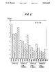
- FIG. 2 is a bar graph setting forth data to illustrate benefits achieved through the use of the invention.
- FIG. 3A, 3B, 3C and 3D are microphotographs illustrating the cross-sectional configurations of foils produced in accordance with the invention.
- the present invention provides a method for manufacturing copper foil products by electrodeposition wherein a number of important physical properties and characteristics of the foil may be closely controlled.
- the invention provides for the electrodeposition of copper foil by cathodic electrodeposition from an electrolyte solution containing copper ions, sulphate ions and a gelatine component and to which is added a copper foil characteristics controlling quantity of an active sulphur containing component.
- the active sulphur containing component which preferably may be thiourea or some other component having a bivalent sulphur atom, both bonds of which are directly connected to a carbon atom together with one or more nitrogen atoms also directly connected to the carbon atom, provides a mechanism for achieving close control of certain critical characteristics of the electrodepositing foil during the conduct of the electrodepositing operation.
- the roughness, elongation and tensile strength of copper foil may each be manipulated and controlled. As a result it is often also possible to achieve an increase in current density.
- An electroplating operation conducting in accordance with the invention may be carried out in a continuous electroplating system of the sort depicted schematically in FIG. 1 of the drawings.
- the system includes an electroforming cell (EFC) 10 that comprises an anode 12, a cathode 14, a vessel 16 and an electrolyte solution 18 contained in vessel 16 and in which anode 12 and cathode 14 are suitably submerged.
- EFC electroforming cell
- Solution 18 contains copper ions, sulphate ions, a gelatine component and an active sulphur containing component and means are provided, in a manner that is well known in the art, for applying an electrical current between anode 12 and cathode 14.
- copper ions in solution 18 gain electrons at the peripheral surface 14a of cathode 14 whereby metallic copper plates out in the form of a foil layer web 20.
- Cathode 14 rotates continuously about its axis 14b during the process and foil layer 20 is continuously withdrawn from surface 14a and thus from EPC 10 as a continuous web which is formed into a roll 20a.
- the process depletes the eleotrolyte solution of copper ions, sulphate ions, the gelatine component and the active sulphur containing component. And since the process is preferably a continuous process these ingredients must be continuously replenished.
- solution 18 is withdrawn through line 22 and recirculated through a filter 24, a digester 26 and another filter 28 and then is reintroduced into vessel 16 through line 30.
- Sulphuric acid from a source 32 is fed into digester 26 through line 34 and metallic copper from a source 36 is introduced into digester 26 as indicated schematically along the path 38.
- Metallic copper is digested by sulphuric acid to form copper ions in digester 26.
- Make-up gelatine component is added to the recirculating solution in line 22 from a source 40 through a line 42.
- the active sulphur containing component is added to the recirculating solution in line 30 through line 44 from a source 46.
- the sulphur containing component is preferably introduced into the recirculating solution at a point as near to the vessel 16 as possible to minimize decomposition of the active sulphur containing component by the highly acidic recirculating fluid existing from digester 26.
- chloride ion is a common contaminant in water and in bulk ingredients.
- the chloride ion concentration has an effect on the properties of the electroplated foil it is desirable to control the chloride ion concentration at a known level to eliminate the uncertainties that would be involved if the chloride ion concentration were to fluctuate unpredictably.
- the chloride ion concentration in the electrolyte is in the range of from about 20 to about 200 ppm, preferably from about 30 to about 100 ppm, and ideally about 80 ppm.
- the chloride ion content in the electrolyte solution may be controlled by devices that are well known and conventionally employed by those of ordinary skill in the art of production of conductive foils by electroforming processes.
- the concentrations of the active sulphur containing component and the gelatine component in the electrolyte solution may preferably be expressed in terms of the steady state consumption rate thereof.
- These ingredients act at the surface of the copper foil as it forms and are consumed by the reactions which occur there. And they affect the internal regions as well as the external surfaces of the foil and thus have a modifying effect on tensile strength, ductility and elongation in addition to surface roughness.
- the consumption rate is determined by the concentration of each ingredient in the electrolyte solution and this is determined by the amount of each ingredient that is added to the electrolyte solution during steady state operation.
- the addition rate may be expressed in terms of weight added per unit of time per unit of current flow.
- the addition rate of the active sulphur containing component and of the gelatine component may be defined as milligrams added to the electrolyte solution per minute per one thousand amperes (mg/min.kA).
- gelatine components are discussed and defined in the E. H. Chia et al. and S. E. Afifi et al. articles cited above.
- useful gelatine components are high-protein polymers of amino acids linked by peptide chains, --CO--NH--, and having molecular weights in the range of from about 10,000 to 300,000.
- Commonly animal glue is used as the gelatine component because it is relatively inexpensive, readily commercially available and convenient to handle.
- Thiourea is effectively used as an active sulphur containing additive for an electrolyte solution that also contains both animal glue as a gelatine component and chloride ions and which is used to electrolytically produce copper foil having uniform controlled roughness.
- the chloride ion level in the solution may preferably be controlled at about 80 ppm.
- the animal glue itself is often incapable of effectively producing a desired degree of leveling and smoothness of the deposit and the addition of thiourea produces a substantial roughness controlling effect. The lowering of the roughness by the thiourea is thought to occur by a surface adsorption which affects the morphology of the growing deposit front.
- low profile IPC Class 1 foil may conveniently be produced.
- the foils produced in accordance with the invention may have lower roughness, slightly elevated tensile strength, slightly lower elongation characteristics and TD and LD properties that are more isotropic.
- TD properties are measured across the web, that is, in a direction parallel to the axis of rotation of cathode drum 14, while LD properties are measured in a direction along the web.
- EFC 10 of FIG. 1 may be operated at increased current densities to thereby increase the commercial output of the process.
- the tensile strength of the Class 1 foil may be higher and the modulus of elasticity may also be higher than when animal glue alone is used to control roughness.
- Such foil having higher tensile strength and higher modulus of elasticity is less susceptible to wrinkling. The net result of this in a commercial application is that less foil will be damaged during processing and waste will thereby be reduced.
- FIGS. 3A through 3D of the drawings where 3A shows the cross-section of a foil electrodeposited from an electrolyte bath containing 2 ppm animal glue and 0 ppm thiourea; FIG. 3B shows the cross-section of a foil electrodeposited from a bath containing 2 ppm animal glue and 1 ppm thiourea; FIG. 3C shows the cross-section of a foil electrodeposited from a bath containing 2 ppm animal glue and 2 ppm thiourea; and FIG. 3D shows the cross-section of a foil electrodeposited from a bath containing 2 ppm animal glue and 3 ppm thiourea.
- the leveling power of the thiourea is clearly evident from FIGS. 3A through 3D.
- a glue concentration in the order of 2 ppm is generally used to produce IPC Class 1 foils.
- the glue level is increased to reduce roughness and produce low profile foil.
- the glue level is decreased to produce IPC Class 3 foils.
- an increase in the level of thiourea results in an increase in tensile strength and decreases in both roughness and elongation.
- an increase in current density results in a decrease in elongation and increases in both tensile strength and roughness.
- an increase in the glue level results in an increase in tensile strength and decreases in both roughness and elongation.
- IPC Class 1 low profile foil may be produced, in accordance with the invention, without the need for decreasing current densities and without loss of metallurgical properties.
- R tm roughness may be decreased to provide a Class 1 low profile foil
- Tensile strength may be increased and the modulus of elasticity also increased to provide a wrinkle resistant Class 1 foil;
- R tm roughness may be decreased to provide a Class 3 low profile foil
- Elongation may be increased to provide an improved Class 3 foil
- IPC Class 3 2 oz. foil may be produced in an EFC 10 as depicted in FIG. 1 as follows:
Landscapes
- Chemical & Material Sciences (AREA)
- Engineering & Computer Science (AREA)
- Organic Chemistry (AREA)
- Electrochemistry (AREA)
- Materials Engineering (AREA)
- Metallurgy (AREA)
- Chemical Kinetics & Catalysis (AREA)
- Microelectronics & Electronic Packaging (AREA)
- Electroplating Methods And Accessories (AREA)
- Electroplating And Plating Baths Therefor (AREA)
- Parts Printed On Printed Circuit Boards (AREA)
- Electrolytic Production Of Metals (AREA)
- Manufacturing Of Printed Wiring (AREA)
- Chemically Coating (AREA)
Priority Applications (15)
| Application Number | Priority Date | Filing Date | Title |
|---|---|---|---|
| US07/406,894 US5215645A (en) | 1989-09-13 | 1989-09-13 | Electrodeposited foil with controlled properties for printed circuit board applications and procedures and electrolyte bath solutions for preparing the same |
| US07/510,231 US5171417A (en) | 1989-09-13 | 1990-04-18 | Copper foils for printed circuit board applications and procedures and electrolyte bath solutions for electrodepositing the same |
| JP2512781A JP3058445B2 (ja) | 1989-09-13 | 1990-09-12 | 特性の調整された、印刷回路基板用の電着された箔並びにそれを製造するための方法及び電解槽溶液 |
| BR909006918A BR9006918A (pt) | 1989-09-13 | 1990-09-12 | Processo para formar,eletroliticamente,uma lamina de cobre para aplicacoes em quadro de circuito impresso,banho eletrolitico para depositar,eletroliticamente,lamina de cobre para aplicacao em quadro de circuito impresso e lamina de cobre |
| AU63417/90A AU640169B2 (en) | 1989-09-13 | 1990-09-12 | Electrodeposited foil with controlled properties for printed circuit board applications and procedures and electrolyte bath solutions for preparing the same |
| HU907373A HU210114B (en) | 1989-09-13 | 1990-09-12 | Process and electrolyte bath solutions for preparing electrodeposited foil for printed circuit board applications |
| IE332290A IE903322A1 (en) | 1989-09-13 | 1990-09-12 | Electrodeposited foil with controlled properties for printed¹circuit board applications and procedures and electrolyte¹bath solutions for preparing the same |
| EP90913685A EP0443009B1 (de) | 1989-09-13 | 1990-09-12 | Elektrobeschichtete folien mit bestimmten eigenschaften für gedruckte schaltungen sowie verfahren und elektrolysebadlösungen zu ihrer herstellung |
| CA002041665A CA2041665A1 (en) | 1989-09-13 | 1990-09-12 | Electrodeposited foil with controlled properties for printed circuit board applications and procedures and electrolyte bath solutions for preparing the same |
| KR1019910700486A KR920701526A (ko) | 1989-09-13 | 1990-09-12 | 인쇄회로기판에 사용하기 위한 조절된 특성을 갖는 전착 포일(electrodeposited foil), 그 제조방법 및 전착포일 제조용 전해조용액 |
| PCT/US1990/005162 WO1991004358A1 (en) | 1989-09-13 | 1990-09-12 | Electrodeposited foil with controlled properties for printed circuit board applications and procedures and electrolyte bath solutions for preparing the same |
| DE69031905T DE69031905T2 (de) | 1989-09-13 | 1990-09-12 | Elektrobeschichtete folien mit bestimmten eigenschaften für gedruckte schaltungen sowie verfahren und elektrolysebadlösungen zu ihrer herstellung |
| CN90108444A CN1093179C (zh) | 1989-09-13 | 1990-09-12 | 用于印刷电路板且其性质得到控制的箔片以及生产该箔片的工艺方法和电解液 |
| MYPI90001579A MY107259A (en) | 1989-09-13 | 1990-09-13 | Electrodeposited foil with controlled properties for printed circuit board applications and procedures and electrolyte bath solutions for preparing the same. |
| IL9567290A IL95672A (en) | 1989-09-13 | 1990-09-13 | Copper foil for printed circuit, processes for its preparation and electrolytic bath solutions for investment by electricity |
Applications Claiming Priority (1)
| Application Number | Priority Date | Filing Date | Title |
|---|---|---|---|
| US07/406,894 US5215645A (en) | 1989-09-13 | 1989-09-13 | Electrodeposited foil with controlled properties for printed circuit board applications and procedures and electrolyte bath solutions for preparing the same |
Related Child Applications (1)
| Application Number | Title | Priority Date | Filing Date |
|---|---|---|---|
| US07/510,231 Continuation-In-Part US5171417A (en) | 1989-09-13 | 1990-04-18 | Copper foils for printed circuit board applications and procedures and electrolyte bath solutions for electrodepositing the same |
Publications (1)
| Publication Number | Publication Date |
|---|---|
| US5215645A true US5215645A (en) | 1993-06-01 |
Family
ID=23609806
Family Applications (1)
| Application Number | Title | Priority Date | Filing Date |
|---|---|---|---|
| US07/406,894 Expired - Lifetime US5215645A (en) | 1989-09-13 | 1989-09-13 | Electrodeposited foil with controlled properties for printed circuit board applications and procedures and electrolyte bath solutions for preparing the same |
Country Status (14)
| Country | Link |
|---|---|
| US (1) | US5215645A (de) |
| EP (1) | EP0443009B1 (de) |
| JP (1) | JP3058445B2 (de) |
| KR (1) | KR920701526A (de) |
| CN (1) | CN1093179C (de) |
| AU (1) | AU640169B2 (de) |
| BR (1) | BR9006918A (de) |
| CA (1) | CA2041665A1 (de) |
| DE (1) | DE69031905T2 (de) |
| HU (1) | HU210114B (de) |
| IE (1) | IE903322A1 (de) |
| IL (1) | IL95672A (de) |
| MY (1) | MY107259A (de) |
| WO (1) | WO1991004358A1 (de) |
Cited By (20)
| Publication number | Priority date | Publication date | Assignee | Title |
|---|---|---|---|---|
| WO1994024338A1 (en) * | 1993-04-19 | 1994-10-27 | Magma Copper Company | Process for making copper foil |
| US5509557A (en) * | 1994-01-24 | 1996-04-23 | International Business Machines Corporation | Depositing a conductive metal onto a substrate |
| WO1996013624A1 (en) * | 1994-10-26 | 1996-05-09 | Magma Copper Company | Process for making copper wire |
| US5679232A (en) * | 1993-04-19 | 1997-10-21 | Electrocopper Products Limited | Process for making wire |
| WO1998008361A1 (en) * | 1996-08-23 | 1998-02-26 | Gould Electronics Inc. | High performance flexible laminate |
| US5830583A (en) * | 1993-04-19 | 1998-11-03 | Clouser; Sidney J. | Copper wire |
| US5834140A (en) * | 1995-09-22 | 1998-11-10 | Circuit Foil Japan Co., Ltd. | Electrodeposited copper foil for fine pattern and method for producing the same |
| US5863666A (en) * | 1997-08-07 | 1999-01-26 | Gould Electronics Inc. | High performance flexible laminate |
| US6123788A (en) * | 1993-04-19 | 2000-09-26 | Electrocopper Products Limited | Copper wire and process for making copper wire |
| US20020137256A1 (en) * | 2001-03-26 | 2002-09-26 | International Business Machines Corporation | Method and structure for an organic package with improved BGA life |
| US20030168651A1 (en) * | 2001-10-26 | 2003-09-11 | Kozicki Michael N. | Programmable surface control devices and method of making same |
| US6676823B1 (en) | 2002-03-18 | 2004-01-13 | Taskem, Inc. | High speed acid copper plating |
| US20040050707A1 (en) * | 2001-01-22 | 2004-03-18 | Hans Warlimont | Continuous electroforming process to form a strip for battery electrodes and a mandrel to be used in said electroforming process |
| US20040187731A1 (en) * | 1999-07-15 | 2004-09-30 | Wang Qing Min | Acid copper electroplating solutions |
| US20050266756A1 (en) * | 2004-06-01 | 2005-12-01 | Isola Laminate Systems Corp. | Laminate composition for producing reduced curl flat thin core laminate |
| US20070190822A1 (en) * | 2006-02-09 | 2007-08-16 | General Dynamics Advanced Information Systems, Inc. | Low profile compliant leads |
| EP2113587A1 (de) | 2008-04-28 | 2009-11-04 | ATOTECH Deutschland GmbH | Wässriges saures Bad und Verfahren zum elektronischen Abschneiden von Kupfer |
| US20110003269A1 (en) * | 2007-06-11 | 2011-01-06 | Rocco Portoghese | Infrared aimpoint detection system |
| US20140316551A1 (en) * | 2011-12-23 | 2014-10-23 | Hexcel Composites Limited | Method for on-line control of a manufacturing process for a multicomponent sheet material |
| US9138964B2 (en) | 2010-11-22 | 2015-09-22 | Mitsui Mining & Smelting Co., Ltd | Surface-treated copper foil |
Families Citing this family (14)
| Publication number | Priority date | Publication date | Assignee | Title |
|---|---|---|---|---|
| KR100275899B1 (ko) * | 1990-05-30 | 2000-12-15 | 마이클 에이. 센타니 | 전착구리호일 및 클로라이드(chloride) 이온농도가 낮은 전해액을 사용하여 이를 제조하는 방법 |
| US5403465A (en) * | 1990-05-30 | 1995-04-04 | Gould Inc. | Electrodeposited copper foil and process for making same using electrolyte solutions having controlled additions of chloride ions and organic additives |
| EP0695377B1 (de) * | 1993-04-19 | 2001-06-27 | GA-TEK Inc. | Verfahren zur herstellung von kupfermetallpulver kupferoxide und kupferfolie |
| US5670033A (en) * | 1993-04-19 | 1997-09-23 | Electrocopper Products Limited | Process for making copper metal powder, copper oxides and copper foil |
| JPH10330983A (ja) | 1997-05-30 | 1998-12-15 | Fukuda Metal Foil & Powder Co Ltd | 電解銅箔及びその製造方法 |
| US6895299B2 (en) * | 2001-10-16 | 2005-05-17 | Brigham Young University | Systems and methods for representing complex n-curves for direct control of tool motion |
| JP5116943B2 (ja) * | 2003-02-04 | 2013-01-09 | 古河電気工業株式会社 | 高周波回路用銅箔及びその製造方法 |
| CN100564606C (zh) * | 2005-12-06 | 2009-12-02 | 安泰科技股份有限公司 | 金属薄膜连续电沉积装置及其方法 |
| CN102797020A (zh) * | 2011-05-23 | 2012-11-28 | 建滔(连州)铜箔有限公司 | 一种厚规格低峰值的电解铜箔的制备方法 |
| JP5858849B2 (ja) * | 2012-03-30 | 2016-02-10 | Jx日鉱日石金属株式会社 | 金属箔 |
| JP6067256B2 (ja) * | 2012-06-27 | 2017-01-25 | 古河電気工業株式会社 | 電解銅箔、リチウムイオン二次電池用負極電極及びリチウムイオン二次電池 |
| CN105603501A (zh) * | 2016-01-17 | 2016-05-25 | 莫镇威 | 电解铜箔表面处理添加剂、制备方法、处理方法及装置 |
| CN110629257A (zh) * | 2019-07-05 | 2019-12-31 | 九江德福科技股份有限公司 | 一种高抗拉锂电铜箔的制造方法 |
| CN112501658B (zh) * | 2020-12-08 | 2024-10-18 | 九江德福科技股份有限公司 | 一种高模量铜箔生产工艺 |
Citations (5)
| Publication number | Priority date | Publication date | Assignee | Title |
|---|---|---|---|---|
| US2563360A (en) * | 1941-05-24 | 1951-08-07 | Gen Motors Corp | Electrodeposition of copper |
| US3923109A (en) * | 1975-02-24 | 1975-12-02 | Jr Edward B Williams | Drill tool |
| JPS5233074A (en) * | 1975-09-10 | 1977-03-12 | Nippon Mining Co | Surface treatment of printed circuit copper foil |
| JPS63310990A (ja) * | 1987-06-15 | 1988-12-19 | Nippon Denkai Kk | 電解銅箔の製造方法 |
| JPS63310989A (ja) * | 1987-06-15 | 1988-12-19 | Nippon Denkai Kk | 電解銅箔の製造方法 |
Family Cites Families (6)
| Publication number | Priority date | Publication date | Assignee | Title |
|---|---|---|---|---|
| US3293109A (en) * | 1961-09-18 | 1966-12-20 | Clevite Corp | Conducting element having improved bonding characteristics and method |
| US3389064A (en) * | 1964-07-22 | 1968-06-18 | Canadian Copper Refiners Ltd | Electrolytic refining of copper and tank house electrolyte useful therein |
| US3930962A (en) * | 1975-02-21 | 1976-01-06 | Kennecott Copper Corporation | Process and apparatus for producing thin copper foils on a molybdenum or tzm alloy drum |
| HU208556B (en) * | 1985-12-24 | 1993-11-29 | Gould Inc | Process and apparatjus for galvanizing copper-folia |
| JPS6310990A (ja) * | 1986-07-02 | 1988-01-18 | Matsushita Electric Ind Co Ltd | ビデオカメラ |
| JPH05233074A (ja) * | 1992-02-25 | 1993-09-10 | Dai Ichi Seiyaku Co Ltd | pH制御方法及びその装置 |
-
1989
- 1989-09-13 US US07/406,894 patent/US5215645A/en not_active Expired - Lifetime
-
1990
- 1990-09-12 EP EP90913685A patent/EP0443009B1/de not_active Expired - Lifetime
- 1990-09-12 IE IE332290A patent/IE903322A1/en unknown
- 1990-09-12 CN CN90108444A patent/CN1093179C/zh not_active Expired - Lifetime
- 1990-09-12 CA CA002041665A patent/CA2041665A1/en not_active Abandoned
- 1990-09-12 DE DE69031905T patent/DE69031905T2/de not_active Expired - Lifetime
- 1990-09-12 WO PCT/US1990/005162 patent/WO1991004358A1/en not_active Ceased
- 1990-09-12 JP JP2512781A patent/JP3058445B2/ja not_active Expired - Lifetime
- 1990-09-12 HU HU907373A patent/HU210114B/hu not_active IP Right Cessation
- 1990-09-12 AU AU63417/90A patent/AU640169B2/en not_active Ceased
- 1990-09-12 BR BR909006918A patent/BR9006918A/pt not_active Application Discontinuation
- 1990-09-12 KR KR1019910700486A patent/KR920701526A/ko not_active Withdrawn
- 1990-09-13 IL IL9567290A patent/IL95672A/en not_active IP Right Cessation
- 1990-09-13 MY MYPI90001579A patent/MY107259A/en unknown
Patent Citations (5)
| Publication number | Priority date | Publication date | Assignee | Title |
|---|---|---|---|---|
| US2563360A (en) * | 1941-05-24 | 1951-08-07 | Gen Motors Corp | Electrodeposition of copper |
| US3923109A (en) * | 1975-02-24 | 1975-12-02 | Jr Edward B Williams | Drill tool |
| JPS5233074A (en) * | 1975-09-10 | 1977-03-12 | Nippon Mining Co | Surface treatment of printed circuit copper foil |
| JPS63310990A (ja) * | 1987-06-15 | 1988-12-19 | Nippon Denkai Kk | 電解銅箔の製造方法 |
| JPS63310989A (ja) * | 1987-06-15 | 1988-12-19 | Nippon Denkai Kk | 電解銅箔の製造方法 |
Non-Patent Citations (12)
| Title |
|---|
| Afifi, et al, Journal of Metals, Feb. 1987, pp. 38 41. * |
| Afifi, et al, Journal of Metals, Feb. 1987, pp. 38-41. |
| Bucci, et al. "Foil Technology for PCB Fabrication: Foil Manufacturing & Developement for Advanced PCB Designs", presented at PCFAC EXPO '86 (May 12, 1986). |
| Bucci, et al. Foil Technology for PCB Fabrication: Foil Manufacturing & Developement for Advanced PCB Designs , presented at PCFAC EXPO 86 (May 12, 1986). * |
| Chia, et al, Journal of Metals, Apr. 1987, pp. 42 45. * |
| Chia, et al, Journal of Metals, Apr. 1987, pp. 42-45. |
| Franklin, Surface and Coating Technology, 30, (1987) pp. 415 428. * |
| Franklin, Surface and Coating Technology, 30, (1987) pp. 415-428. |
| Ibl et al, Electrochimica Acta, 1972, vol. 17, pp. 733 739. * |
| Ibl et al, Electrochimica Acta, 1972, vol. 17, pp. 733-739. |
| Knuutila, et al. "The Effect of Organic Additives on the Electrocrystallization of Copper", 1987, pp. 129-143. |
| Knuutila, et al. The Effect of Organic Additives on the Electrocrystallization of Copper , 1987, pp. 129 143. * |
Cited By (35)
| Publication number | Priority date | Publication date | Assignee | Title |
|---|---|---|---|---|
| US6123788A (en) * | 1993-04-19 | 2000-09-26 | Electrocopper Products Limited | Copper wire and process for making copper wire |
| US5366612A (en) * | 1993-04-19 | 1994-11-22 | Magma Copper Company | Process for making copper foil |
| US5516408A (en) * | 1993-04-19 | 1996-05-14 | Magma Copper Company | Process for making copper wire |
| US5679232A (en) * | 1993-04-19 | 1997-10-21 | Electrocopper Products Limited | Process for making wire |
| WO1994024338A1 (en) * | 1993-04-19 | 1994-10-27 | Magma Copper Company | Process for making copper foil |
| US5830583A (en) * | 1993-04-19 | 1998-11-03 | Clouser; Sidney J. | Copper wire |
| CN1097643C (zh) * | 1993-04-19 | 2003-01-01 | Ga-Tek公司 | 制造铜箔的方法 |
| US5509557A (en) * | 1994-01-24 | 1996-04-23 | International Business Machines Corporation | Depositing a conductive metal onto a substrate |
| WO1996013624A1 (en) * | 1994-10-26 | 1996-05-09 | Magma Copper Company | Process for making copper wire |
| US5834140A (en) * | 1995-09-22 | 1998-11-10 | Circuit Foil Japan Co., Ltd. | Electrodeposited copper foil for fine pattern and method for producing the same |
| RU2149225C1 (ru) * | 1996-04-18 | 2000-05-20 | Электрокоппер Продактс Лимитед | Способ изготовления проволоки |
| WO1998008361A1 (en) * | 1996-08-23 | 1998-02-26 | Gould Electronics Inc. | High performance flexible laminate |
| US5863666A (en) * | 1997-08-07 | 1999-01-26 | Gould Electronics Inc. | High performance flexible laminate |
| US20040187731A1 (en) * | 1999-07-15 | 2004-09-30 | Wang Qing Min | Acid copper electroplating solutions |
| US20040050707A1 (en) * | 2001-01-22 | 2004-03-18 | Hans Warlimont | Continuous electroforming process to form a strip for battery electrodes and a mandrel to be used in said electroforming process |
| US7097754B2 (en) * | 2001-01-22 | 2006-08-29 | Dsl Dresden Material-Innovation Gmbh | Continuous electroforming process to form a strip for battery electrodes and a mandrel to be used in said electroforming process |
| US7615477B2 (en) | 2001-03-26 | 2009-11-10 | International Business Machines Corporation | Method of fabricating a BGA package having decreased adhesion |
| US20020137256A1 (en) * | 2001-03-26 | 2002-09-26 | International Business Machines Corporation | Method and structure for an organic package with improved BGA life |
| US7148566B2 (en) | 2001-03-26 | 2006-12-12 | International Business Machines Corporation | Method and structure for an organic package with improved BGA life |
| US20070099342A1 (en) * | 2001-03-26 | 2007-05-03 | Knickerbocker John U | Method and Structure for an Organic Package with Improved BGA Life |
| US20030168651A1 (en) * | 2001-10-26 | 2003-09-11 | Kozicki Michael N. | Programmable surface control devices and method of making same |
| US7227169B2 (en) * | 2001-10-26 | 2007-06-05 | Arizona Board Of Regents | Programmable surface control devices and method of making same |
| US6676823B1 (en) | 2002-03-18 | 2004-01-13 | Taskem, Inc. | High speed acid copper plating |
| US8263225B2 (en) * | 2004-06-01 | 2012-09-11 | Isola Usa Corp. | Laminate composition for producing reduced curl flat thin core laminate |
| US20050266756A1 (en) * | 2004-06-01 | 2005-12-01 | Isola Laminate Systems Corp. | Laminate composition for producing reduced curl flat thin core laminate |
| US20070190822A1 (en) * | 2006-02-09 | 2007-08-16 | General Dynamics Advanced Information Systems, Inc. | Low profile compliant leads |
| US8481862B2 (en) | 2006-02-09 | 2013-07-09 | General Dynamics Advanced Information Systems, Inc. | Low profile compliant leads |
| US20110003269A1 (en) * | 2007-06-11 | 2011-01-06 | Rocco Portoghese | Infrared aimpoint detection system |
| WO2009132861A3 (en) * | 2008-04-28 | 2010-04-15 | Atotech Deutschland Gmbh | Aqueous, acid bath and method for the electrolytic deposition of copper |
| US20110011746A1 (en) * | 2008-04-28 | 2011-01-20 | Atotech Deutschland Gmbh | Aqueous, Acid Bath and Method for the Electrolytic Deposition of Copper |
| EP2113587A1 (de) | 2008-04-28 | 2009-11-04 | ATOTECH Deutschland GmbH | Wässriges saures Bad und Verfahren zum elektronischen Abschneiden von Kupfer |
| US8679316B2 (en) | 2008-04-28 | 2014-03-25 | Atotech Deutschland Gmbh | Aqueous, acid bath and method for the electrolytic deposition of copper |
| US9138964B2 (en) | 2010-11-22 | 2015-09-22 | Mitsui Mining & Smelting Co., Ltd | Surface-treated copper foil |
| US20140316551A1 (en) * | 2011-12-23 | 2014-10-23 | Hexcel Composites Limited | Method for on-line control of a manufacturing process for a multicomponent sheet material |
| US9675990B2 (en) * | 2011-12-23 | 2017-06-13 | Hexcel Composites Limited | Method for on-line control of a manufacturing process for a multicomponent sheet material |
Also Published As
| Publication number | Publication date |
|---|---|
| JPH04501887A (ja) | 1992-04-02 |
| CA2041665A1 (en) | 1991-03-14 |
| AU640169B2 (en) | 1993-08-19 |
| HUT59185A (en) | 1992-04-28 |
| BR9006918A (pt) | 1991-11-26 |
| DE69031905D1 (de) | 1998-02-12 |
| IE903322A1 (en) | 1991-04-10 |
| WO1991004358A1 (en) | 1991-04-04 |
| CN1053818A (zh) | 1991-08-14 |
| IL95672A (en) | 1996-06-18 |
| MY107259A (en) | 1995-10-31 |
| KR920701526A (ko) | 1992-08-11 |
| IL95672A0 (en) | 1991-06-30 |
| AU6341790A (en) | 1991-04-18 |
| JP3058445B2 (ja) | 2000-07-04 |
| EP0443009A1 (de) | 1991-08-28 |
| HU210114B (en) | 1995-02-28 |
| HU907373D0 (en) | 1991-08-28 |
| EP0443009A4 (en) | 1993-04-14 |
| CN1093179C (zh) | 2002-10-23 |
| DE69031905T2 (de) | 1998-04-16 |
| EP0443009B1 (de) | 1998-01-07 |
Similar Documents
| Publication | Publication Date | Title |
|---|---|---|
| US5215645A (en) | Electrodeposited foil with controlled properties for printed circuit board applications and procedures and electrolyte bath solutions for preparing the same | |
| US5171417A (en) | Copper foils for printed circuit board applications and procedures and electrolyte bath solutions for electrodepositing the same | |
| EP0485588B1 (de) | ELEKTROPLATTIERTE KUPFERFOLIE UND DEREN HERSTELLUNG UNTER VERWENDUNG ELEKTROLYTISCHER LöSUNGEN MIT NIEDRIGEN KONZENTRATIONEN VON CHLOR IONEN | |
| EP0649917B1 (de) | Elektroplattierte Kupferfolie und Verfahren zu deren Herstellung | |
| US5403465A (en) | Electrodeposited copper foil and process for making same using electrolyte solutions having controlled additions of chloride ions and organic additives | |
| US9307639B2 (en) | Electro-deposited copper foil, surface-treated copper foil using the electro-deposited copper foil and copper clad laminate using the surface-treated copper foil, and a method for manufacturing the electro-deposited copper foil | |
| EP0709494B1 (de) | Verfahren zur Oberflächen-Aufrauhung von Kupferfolie | |
| KR102655111B1 (ko) | 표면처리 전해동박, 이의 제조방법, 및 이의 용도 | |
| US3769179A (en) | Copper plating process for printed circuits | |
| US5840170A (en) | Method for inhibiting the electrodeposition of organic particulate matter on copper foil | |
| KR102681509B1 (ko) | 이중층 전해동박 및 그 제조방법 | |
| CN113802157A (zh) | 一种酸性镀铜mvf350盲孔填孔用药水 | |
| CN120291167B (zh) | 具有双重电解槽的铜箔制备系统、电解铜箔及制备方法 | |
| CN116695187A (zh) | 一种用于制备高抗拉锂电铜箔的电解液 | |
| JP2002294484A (ja) | ピロりん酸銅めっき浴及びピロりん酸亜鉛メッキ浴並びにこれらのメッキ浴を用いたメッキ方法 |
Legal Events
| Date | Code | Title | Description |
|---|---|---|---|
| AS | Assignment |
Owner name: GOULD INC., OHIO Free format text: ASSIGNMENT OF ASSIGNORS INTEREST.;ASSIGNORS:DI FRANCO, DINO F.;CLOUSER, SIDNEY J.;REEL/FRAME:005177/0603 Effective date: 19891006 |
|
| STCF | Information on status: patent grant |
Free format text: PATENTED CASE |
|
| AS | Assignment |
Owner name: GOULD ELECTRONICS INC., OHIO Free format text: ASSIGNMENT OF ASSIGNORS INTEREST;ASSIGNOR:GOULD INC.;REEL/FRAME:006865/0444 Effective date: 19940131 |
|
| FEPP | Fee payment procedure |
Free format text: PAYOR NUMBER ASSIGNED (ORIGINAL EVENT CODE: ASPN); ENTITY STATUS OF PATENT OWNER: LARGE ENTITY |
|
| FPAY | Fee payment |
Year of fee payment: 4 |
|
| FPAY | Fee payment |
Year of fee payment: 8 |
|
| AS | Assignment |
Owner name: NIKKO MATERIALS USA, INC., ARIZONA Free format text: BILL OF SALE AND INSTRUMENT OF ASSIGNMENT AND ASSUMPTION;ASSIGNOR:GOULD ELECTRONICS INC.;REEL/FRAME:014022/0437 Effective date: 20030930 |
|
| FPAY | Fee payment |
Year of fee payment: 12 |