US5232901A - Method of producing superconducting ceramic wire having protective metal coating thereon - Google Patents
Method of producing superconducting ceramic wire having protective metal coating thereon Download PDFInfo
- Publication number
- US5232901A US5232901A US07/665,656 US66565691A US5232901A US 5232901 A US5232901 A US 5232901A US 66565691 A US66565691 A US 66565691A US 5232901 A US5232901 A US 5232901A
- Authority
- US
- United States
- Prior art keywords
- wire
- protective metal
- producing
- glass
- oxide superconducting
- Prior art date
- Legal status (The legal status is an assumption and is not a legal conclusion. Google has not performed a legal analysis and makes no representation as to the accuracy of the status listed.)
- Expired - Fee Related
Links
Images

Classifications
-
- C—CHEMISTRY; METALLURGY
- C04—CEMENTS; CONCRETE; ARTIFICIAL STONE; CERAMICS; REFRACTORIES
- C04B—LIME, MAGNESIA; SLAG; CEMENTS; COMPOSITIONS THEREOF, e.g. MORTARS, CONCRETE OR LIKE BUILDING MATERIALS; ARTIFICIAL STONE; CERAMICS; REFRACTORIES; TREATMENT OF NATURAL STONE
- C04B41/00—After-treatment of mortars, concrete, artificial stone or ceramics; Treatment of natural stone
- C04B41/009—After-treatment of mortars, concrete, artificial stone or ceramics; Treatment of natural stone characterised by the material treated
-
- C—CHEMISTRY; METALLURGY
- C03—GLASS; MINERAL OR SLAG WOOL
- C03C—CHEMICAL COMPOSITION OF GLASSES, GLAZES OR VITREOUS ENAMELS; SURFACE TREATMENT OF GLASS; SURFACE TREATMENT OF FIBRES OR FILAMENTS MADE FROM GLASS, MINERALS OR SLAGS; JOINING GLASS TO GLASS OR OTHER MATERIALS
- C03C10/00—Devitrified glass ceramics, i.e. glass ceramics having a crystalline phase dispersed in a glassy phase and constituting at least 50% by weight of the total composition
- C03C10/009—Devitrified glass ceramics, i.e. glass ceramics having a crystalline phase dispersed in a glassy phase and constituting at least 50% by weight of the total composition having a superconducting crystal phase
-
- C—CHEMISTRY; METALLURGY
- C04—CEMENTS; CONCRETE; ARTIFICIAL STONE; CERAMICS; REFRACTORIES
- C04B—LIME, MAGNESIA; SLAG; CEMENTS; COMPOSITIONS THEREOF, e.g. MORTARS, CONCRETE OR LIKE BUILDING MATERIALS; ARTIFICIAL STONE; CERAMICS; REFRACTORIES; TREATMENT OF NATURAL STONE
- C04B41/00—After-treatment of mortars, concrete, artificial stone or ceramics; Treatment of natural stone
- C04B41/45—Coating or impregnating, e.g. injection in masonry, partial coating of green or fired ceramics, organic coating compositions for adhering together two concrete elements
- C04B41/50—Coating or impregnating, e.g. injection in masonry, partial coating of green or fired ceramics, organic coating compositions for adhering together two concrete elements with inorganic materials
- C04B41/51—Metallising, e.g. infiltration of sintered ceramic preforms with molten metal
- C04B41/5111—Ag, Au, Pd, Pt or Cu
-
- C—CHEMISTRY; METALLURGY
- C04—CEMENTS; CONCRETE; ARTIFICIAL STONE; CERAMICS; REFRACTORIES
- C04B—LIME, MAGNESIA; SLAG; CEMENTS; COMPOSITIONS THEREOF, e.g. MORTARS, CONCRETE OR LIKE BUILDING MATERIALS; ARTIFICIAL STONE; CERAMICS; REFRACTORIES; TREATMENT OF NATURAL STONE
- C04B41/00—After-treatment of mortars, concrete, artificial stone or ceramics; Treatment of natural stone
- C04B41/80—After-treatment of mortars, concrete, artificial stone or ceramics; Treatment of natural stone of only ceramics
- C04B41/81—Coating or impregnation
- C04B41/85—Coating or impregnation with inorganic materials
- C04B41/88—Metals
-
- H—ELECTRICITY
- H10—SEMICONDUCTOR DEVICES; ELECTRIC SOLID-STATE DEVICES NOT OTHERWISE PROVIDED FOR
- H10N—ELECTRIC SOLID-STATE DEVICES NOT OTHERWISE PROVIDED FOR
- H10N60/00—Superconducting devices
- H10N60/01—Manufacture or treatment
- H10N60/0268—Manufacture or treatment of devices comprising copper oxide
- H10N60/0801—Manufacture or treatment of filaments or composite wires
-
- Y—GENERAL TAGGING OF NEW TECHNOLOGICAL DEVELOPMENTS; GENERAL TAGGING OF CROSS-SECTIONAL TECHNOLOGIES SPANNING OVER SEVERAL SECTIONS OF THE IPC; TECHNICAL SUBJECTS COVERED BY FORMER USPC CROSS-REFERENCE ART COLLECTIONS [XRACs] AND DIGESTS
- Y10—TECHNICAL SUBJECTS COVERED BY FORMER USPC
- Y10S—TECHNICAL SUBJECTS COVERED BY FORMER USPC CROSS-REFERENCE ART COLLECTIONS [XRACs] AND DIGESTS
- Y10S505/00—Superconductor technology: apparatus, material, process
- Y10S505/70—High TC, above 30 k, superconducting device, article, or structured stock
- Y10S505/704—Wire, fiber, or cable
-
- Y—GENERAL TAGGING OF NEW TECHNOLOGICAL DEVELOPMENTS; GENERAL TAGGING OF CROSS-SECTIONAL TECHNOLOGIES SPANNING OVER SEVERAL SECTIONS OF THE IPC; TECHNICAL SUBJECTS COVERED BY FORMER USPC CROSS-REFERENCE ART COLLECTIONS [XRACs] AND DIGESTS
- Y10—TECHNICAL SUBJECTS COVERED BY FORMER USPC
- Y10S—TECHNICAL SUBJECTS COVERED BY FORMER USPC CROSS-REFERENCE ART COLLECTIONS [XRACs] AND DIGESTS
- Y10S505/00—Superconductor technology: apparatus, material, process
- Y10S505/725—Process of making or treating high tc, above 30 k, superconducting shaped material, article, or device
- Y10S505/733—Rapid solidification, e.g. quenching, gas-atomizing, melt-spinning, roller-quenching
-
- Y—GENERAL TAGGING OF NEW TECHNOLOGICAL DEVELOPMENTS; GENERAL TAGGING OF CROSS-SECTIONAL TECHNOLOGIES SPANNING OVER SEVERAL SECTIONS OF THE IPC; TECHNICAL SUBJECTS COVERED BY FORMER USPC CROSS-REFERENCE ART COLLECTIONS [XRACs] AND DIGESTS
- Y10—TECHNICAL SUBJECTS COVERED BY FORMER USPC
- Y10S—TECHNICAL SUBJECTS COVERED BY FORMER USPC CROSS-REFERENCE ART COLLECTIONS [XRACs] AND DIGESTS
- Y10S505/00—Superconductor technology: apparatus, material, process
- Y10S505/725—Process of making or treating high tc, above 30 k, superconducting shaped material, article, or device
- Y10S505/739—Molding, coating, shaping, or casting of superconducting material
- Y10S505/74—To form wire or fiber
-
- Y—GENERAL TAGGING OF NEW TECHNOLOGICAL DEVELOPMENTS; GENERAL TAGGING OF CROSS-SECTIONAL TECHNOLOGIES SPANNING OVER SEVERAL SECTIONS OF THE IPC; TECHNICAL SUBJECTS COVERED BY FORMER USPC CROSS-REFERENCE ART COLLECTIONS [XRACs] AND DIGESTS
- Y10—TECHNICAL SUBJECTS COVERED BY FORMER USPC
- Y10S—TECHNICAL SUBJECTS COVERED BY FORMER USPC CROSS-REFERENCE ART COLLECTIONS [XRACs] AND DIGESTS
- Y10S505/00—Superconductor technology: apparatus, material, process
- Y10S505/725—Process of making or treating high tc, above 30 k, superconducting shaped material, article, or device
- Y10S505/742—Annealing
Definitions
- the present invention relates to a method of producing a superconducting wire, and more particularly it relates to a method of producing a superconducting ceramic wire having a protective metal coating thereon.
- a metal oxide ceramic superconducting wire has poor flexibility and is susceptible to quality degradation.
- a protective metal coating or covering has often been made on the surface of such superconducting ceramic wire.
- Japanese Patent Application Publication No. 134819 (Sedaka et al) and European Patent Application Publication No. 285169 (Nakai et al) disclose the covering during so-called melt-drawing method including annealing step to crystallize the drawn wire in one process.
- the former deals with Y-Er-Ba-Cu-O ceramic system, and a coating is effected after annealing step.
- the latter discloses the covering of a variety of ceramic systems including Y-Ba-Cu-O and Bi-Sr-Ca-Cu-O systems, and the covering is effected by leading the melt into a platinum pipe acting as a support.
- U.S. Pat. No. 4,975,416 (to Onishi et al) corresponding to European Patent Application No. 369464 which is incorporated herein by reference discloses a method of producing a superconducting ceramic wire of various systems including Bi-Sr-Ca-Cu-O, Bi-Pb-Sr-Ca-Cu-O, Tl-Ba-Ca-Cu-O and Tl-Bi-Sr-Ca-Cu-O systems, which is called now melt-quenching and preform wire-drawing process in which the starting oxide mixture is molten, quenched to a glass in amorphous state, a preform made of the glass is wire-drawn with keeping amorphous state to a such extremely thin wire as 100 ⁇ m or less and the wire is subjected to heat-treatment to give superconductivity.
- Bi-Sr-Ca-Cu-O Bi-Pb-Sr-Ca-Cu-O
- Tl-Ba-Ca-Cu-O T
- a superconducting ceramic thin wire having higher flexibility and better superconducting properties than those obtained by the above other methods can be realized with excellent productivity.
- the method with its characterization or identification is also published as articles in a Japanese journal by reporters including some of the present inventors. (Japanese Journal of Applied Physics, Vol., 28, No. 12, Dec. 1989; and Vol. 29, No. 1, Jan., 1990, which are also incorporated herein by reference).
- the reference U.S. Pat. No. 4,975,416 also discloses a metal (e.g. Ag)-protecting cover of the resulting superconducting wire.
- a wire which is super conductive is coated or covered with metal by sandwiching between metal plates, inserting in a metal pipe, dipping into a molten metal or winding a metal tape.
- the significance of the covering is not only to improve the poor flexibility of the superconducting wire obtained by the melt-quenching process so as not to be damaged by a slight strain, but also to improve its property.
- the wire is so brittle that a pressure sufficient to enhance the critical current density due to the crystal orientation is differently applied.
- a superconducting state of the superconductor fiber is partially disturbed under the influence of ambient turbulence such as in magnetic field or mechanical strain when a current flows through the fiber. Joule heat is generated by such a portion of the fiber. Since the conventional fiber has a poor heat dissipation property, the temperature of the fiber as a whole is increased to disturb the superconducting state of the entire superconducting state.
- a practical technique for coating Ag on a fiber manufactured by the prior-art method can be a plating method or a dipping method of dipping a fiber into an Ag melt.
- the plating method results in poor productivity.
- the temperature of the Ag melt reaches 961° C. It is impossible to dip a superconducting fiber in the Ag melt because the superconducting fiber is softened at 400° to 500° C.
- the object of the present invention is to provide a simple and inexpensive metal-covering or coating method.
- a method of producing a protective metal coated or covered superconducting ceramic wire which comprises applying a finely pulverized protective metal-dispersed polymeric resin onto the surface of a glass wire in amorphous state which consists essentially of metal oxides capable of being converted into superconductive ceramic, heating the wire to remove the polymeric resin therefrom to obtain the wire having a metal powder coating thereon, and heat-treating the wire to become superconductive.
- FIG. 1A is a view showing an apparatus for realizing a method of manufacturing a superconducting fiber according to an embodiment of the present invention.
- FIG. 1B is a partially sectional view of a superconducting fiber obtained by the apparatus shown in FIG. 1A;
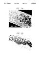
- FIG. 2A is an electron micrograph showing a glass wire obtained by a method according to the present invention.
- FIG. 2B is an electron micrograph showing a glass wire obtained by a method accrding to the present invention.
- a feature of the present invention is that a coating is effected with respect to a glass wire in amorphous state.
- the glass wire is so thin and flexible that it can be wound onto a mandrel of 10 mm diameter, and has almost quantitative density and smooth surface. These demonstrate possibility of giving good coatings by easy processing.
- Another feature is that the heat-treatment for giving superconductivity is conducted to the glass wire having a metal powder coating on the surface.
- any ceramic compositions of the glass wire may be used as far as the glass wire is in amorphous state.
- the systems disclosed in the references previously mentioned may be employed in the invention. More particularly, the above mentioned system Bi-Sr-Cu-Ca-O which may be doped with Pb and/or Ag, and the Tl-Ba-Ca-Cu-O and Tl-Bi-Sr-Ca-Cu-O system are usable as disclosed in the U.S. Pat. No. 4,975,416. Further the Bi-system doped with Nb and/or Sb can be converted to the amprphous state as disclosed in Solid State Communications, Vol. 72, No. 1, pp. 113-116(Rojek et al), 1989 and may be also used in the present invention.
- the glass wire may also be made by any method, and the melt-drawing method disclosed in the Japanese Patent Application Publication No. 134819/1989 would enable to prepare the glass wire if an appropriate device for supercooling the melt-drawn fiber were provided.
- Zheng et al App. Phys. Lett. Vol. 55, No.12, Sep.18, 1989, pp. 1255-1257
- amorphous glass fibers of Bi-Ca-Sr-Cu-O system prepared by melt-spinning, which are then heat-treated to obtain dense superconducting fibers.
- the so-called melt-quenching and preform wire-drawing method as disclosed in the U.S. Pat. No. 4,975,416 is believed to be best.
- the glass wire is coated with a protective layer of metal powders, such as those of Ag, Au, Pt, Cu, Ni, or alloys there of among which Ag is most preferable.
- the coating is carried out by applying a polymeric resin dispersed with the finely pulverized metal powders or foils onto the glass wire surface, followed by drying or hardening the applied surface.
- the application method is in any ways such as brushing, immersing or spraying.
- the metal dispersed resin is preferably in the form of a thermo or photo- hardening varnish or paste.
- the resin used is thermo plastic type which can be vaporized or decomposed completely by heating at a temperature below the glass transition temperature of the wire. Though there may be used any thermo plastic resins such as polyacrylic acid, polyacrylate, polyvinyl alcohol, polyvinyl butyral etc. as far as the above restriction is satisfied, a polyacrylic resin is herein mentioned as an example.
- the coating including the application and hardening is preferably repeated several times to give a thick resin layer onto whole surface of the wire, since the resulting metal coating apts to contract due to subsequent resin removing step by heating.
- the step of removal of the polymeric resin and varnish components from the resin coated and hardened wire is carried out by heating at temperature below the glass transition, and preferably below the crystallization temperature of the wire, leaving a coating of the metal powders.
- temperature is preferably up to 400° C. Higher temperature may be used, but cause deterioration of superconductivity due to the reaction with gas components.
- the heat-treatment to make the thus formed metal coated wire superconductive may preferably be carried out according to the method disclosed in the U.S. Pat. No. 4,975,416 or the European Patent Application Publication No. 369464, which has been incorporated herein by reference as above.
- the wire is kept at a crystal-growing temperature for a considerable time.
- the wire may be subjected to preheat-treatment which forms crystal nuclei. Though the both temperatures will be different depending upon the materials of the wire, the former is about 800° C. to about 870° C. and the latter is about 420° C. to about 430° C. for Bi-Sr-Ca-Cu-O system with or without being doped with Pb or others.
- metal powder-coated superconducting ceramic wire can be subjected to an additional heat-treatment to improve its critical current density, as disclosed in the U.S. Pat. No. 4,975,416.
- the heat-treatment is carried out in same way as above before, during or after application of pressure to cause enhancement of the orientation of crystals to longitudal direction.
- the metal powder coating is most desirable to cover whole surface of the resulting superconducting wire with continuous layer, it is permitted according to the present invention to cover a major part of the surface with a metal powder layer having a minor gap, as far as the protection of wire is substantially achieved.
- the step of coating onto glass wire can be incorporated in the melt-quenching and preform wire-drawing process and effected without damaging the excellent productivity which is the most important characteristic of the process. That is, the resin or varnish can continuously be applied on-line basis onto a very fine, solid glass wire which has been continuously wire-drawn from a preform, as is done in resin coating of optical fibers.
- the protective metal powder or foil coated superconducting wire obtained according to the present invention has an improved flexibility and can eliminate the above drawbacks of the superconducting wire itself prepared by the corresponding method.
- the pressing to improve the critical current density (Jc) the dissipation of Joule heat through the metal coating having a high thermal conductivity and the suppression of evaporation of metal constituent become effective.
- a preform 1 of a ceramic glass prepared by the melt-quenching method is set in an arm 2 in FIG. 1A.
- the arm 2 is connected to a preform driver 3 so that the preform can be vertically driven by the driver 3.
- a heater 4 is arranged to surround the distal end portion of the preform 1, and heats and softens the preform 1 to draw a glass wire 5 with keeping amorphous state.
- the size of the drawn glass wire 5 is measured by a diameter gauge 6, and the glass wire 5 is supplied to a die 7.
- a polymeric resin varnish dispersing a finely pulverized protective Ag is supplied to the die 7, so that the resin is uniformly applied on to the surface of glass wire 5.
- a varnish-coated glass wire 8 passes through a varnish hardening furnace 9.
- a glass wire 10 with the hardened varnish is taken up by a winder 13 through capstans 11 and 12.
- the glass wire 10 with the hardened varnish, which is wound around the winder 13 is placed in an electric furnace (not shown) and is heated at a temperature below the crystallization temperature of the glass wire 5 to remove the varnish component of the coating layer by evaporation or decomposition. Only Ag is left on the surface of the glass wire, thereby obtaining an Ag-glass wire. In this case, coating by means of the die 7 and varnish removal in the electric furnace may be repeated again.
- the resultant wire is heat-treated to form the superconducting crystal phase, thereby obtaining a superconducting wire 20 shown in FIG. 1B.
- the superconducting wire 20 comprises a superconductor portion 21 containing the superconducting crystal phase and a coating portion 22 of Ag powder layer.
- a varnish paste obtained by dispersing Ag in an acrylic resin was applied to the glass wire, and the glass wire was passed through a heating furnace at 100° C. to harden the varnish.
- the glass wire coated with a resin layer dispersing Ag was heated in an electric furnace at 300° C. for 12 hours to evaporate the resin component.
- the wire having Ag layer on its surface was superconducting wire. Brittleness of the wire was improved, and the wire was not broken even at a bending stress of 0.5%. Electrical characteristics of the resultant wire were measured by a known four-terminal method.
- a critical temperature T C and a critical current density J C were as follows:
- a glass wire was prepared according to the procedure of Example 1. The wire was coated by dipping in a Ag powder dispersed acrylic resin paste at room temperature, dried at about 100° C. and heated at 300° C. for about 12 hours to vaporize the paste components.
- FIG. 2A An electron micrograph of the thus resulting glass wire having substantially Ag powder layer on the surface is shown in FIG. 2A.
- the glass wire heat-treated by heating at 840° C. for 100 hours. After cooling to room temperature, the wire was pressed at the pressure of 400 kg/cm 2 to cause the orientation of crystals, and then heat-treated again by heating at 840° C. for 100 hours.
- the critical current density (Jc) was 2000 A/cm 2 at 77 k.
- FIG. 2B An electron micrograph of the thus obtained superconducting wire having Ag powder layer on the surface is shown in FIG. 2B.
- COMPARATIVE EXAMPLE 1 surface is shown in FIG. 2B.
- a superconducting wire was prepared without an Ag coating, following the same procedures as in Example 1.
- the resultant wire was brittle and broken at a small bending stress of 0.1%.
- the characteristics of the fiber measured by the known four-terminal method were as follows:
- the composition of the resultant wire was analyzed by the ICP method. Pb was perfectly evaporated from the wire.
- a glass wire having no coating prepared following the same procedures as in Example 1 was heat-treated to convert into a superconductor material at 423° C. for 4 hours and 840° C. for 100 hours.
- An Ag-containing resin was coated on the wire, following the same procedures as in Example 1. The resin component was evaporated, and another heat treatment was performed at 840° C. for 100 hours. The resultant wire was porous and did not exhibit superconducting properties in all temperature ranges.
Landscapes
- Chemical & Material Sciences (AREA)
- Engineering & Computer Science (AREA)
- Ceramic Engineering (AREA)
- Materials Engineering (AREA)
- Organic Chemistry (AREA)
- Structural Engineering (AREA)
- Inorganic Chemistry (AREA)
- Dispersion Chemistry (AREA)
- Geochemistry & Mineralogy (AREA)
- General Chemical & Material Sciences (AREA)
- Chemical Kinetics & Catalysis (AREA)
- Life Sciences & Earth Sciences (AREA)
- Crystallography & Structural Chemistry (AREA)
- Manufacturing & Machinery (AREA)
- Superconductors And Manufacturing Methods Therefor (AREA)
- Inorganic Compounds Of Heavy Metals (AREA)
- Chemical Or Physical Treatment Of Fibers (AREA)
- Surface Treatment Of Glass Fibres Or Filaments (AREA)
Applications Claiming Priority (2)
| Application Number | Priority Date | Filing Date | Title |
|---|---|---|---|
| JP2-57344 | 1990-03-08 | ||
| JP2057344A JPH03261006A (ja) | 1990-03-08 | 1990-03-08 | 超電導線材の製造方法 |
Publications (1)
| Publication Number | Publication Date |
|---|---|
| US5232901A true US5232901A (en) | 1993-08-03 |
Family
ID=13052957
Family Applications (1)
| Application Number | Title | Priority Date | Filing Date |
|---|---|---|---|
| US07/665,656 Expired - Fee Related US5232901A (en) | 1990-03-08 | 1991-03-07 | Method of producing superconducting ceramic wire having protective metal coating thereon |
Country Status (4)
| Country | Link |
|---|---|
| US (1) | US5232901A (de) |
| EP (1) | EP0445832B1 (de) |
| JP (1) | JPH03261006A (de) |
| DE (1) | DE69110504T2 (de) |
Cited By (3)
| Publication number | Priority date | Publication date | Assignee | Title |
|---|---|---|---|---|
| US5330969A (en) * | 1991-02-06 | 1994-07-19 | Iowa State University Research Foundation, Inc. | Method for producing strain tolerant multifilamentary oxide superconducting wire |
| WO1997022127A1 (en) * | 1995-12-12 | 1997-06-19 | Owens Corning | Method for making superconducting fibers |
| KR100742295B1 (ko) | 2006-03-06 | 2007-07-24 | 한국생산기술연구원 | 연속주조법에 의한 Ni-W 초전도체 제조방법 |
Families Citing this family (4)
| Publication number | Priority date | Publication date | Assignee | Title |
|---|---|---|---|---|
| CA2134466A1 (en) * | 1992-04-28 | 1993-11-11 | George E. Zahr | Method for dispersion spinning of sheathed rod-in-tube superconducting composites |
| DE4304573A1 (de) * | 1993-02-16 | 1994-08-18 | Forschungsgesellschaft Fuer In | Passivierungsschicht für Hochtemperatur-Supraleiter und Verfahren zu ihrer Aufbringung |
| US5413753A (en) * | 1993-09-17 | 1995-05-09 | E. I. Du Pont De Nemours And Company | Method for dispersion spinning of sheathed rod-in-tube superconducting composites |
| DE4339407A1 (de) * | 1993-11-18 | 1995-05-24 | Dresden Ev Inst Festkoerper | Verfahren zur Herstellung von bandförmigen Hochtemperatur-Supraleitern |
Citations (8)
| Publication number | Priority date | Publication date | Assignee | Title |
|---|---|---|---|---|
| EP0285168A2 (de) * | 1987-04-02 | 1988-10-05 | Sumitomo Electric Industries Limited | Supraleitender Draht und Verfahren zu seiner Herstellung |
| EP0292125A1 (de) * | 1987-04-27 | 1988-11-23 | Fujitsu Limited | Mehrschichtiges supraleitendes Substrat für Schaltkreise und dessen Herstellungsprozess |
| JPS6412427A (en) * | 1987-07-06 | 1989-01-17 | Showa Electric Wire & Cable Co | Manufacture of ceramic-based superconducting wire |
| EP0306034A2 (de) * | 1987-09-04 | 1989-03-08 | W.R. Grace & Co.-Conn. | Verfahren und Zusammensetzung zur Darstellung supraleitender Keramik und anderer keramischer Materalien mit verringertem elektrischem Widerstand und elektrisch leitende plattierte metallische Produkte daraus |
| EP0305949A1 (de) * | 1987-08-28 | 1989-03-08 | Mitsubishi Materials Corporation | Verfahren zur Herstellung supraleitender keramischer Materialien |
| JPH01134819A (ja) * | 1987-11-18 | 1989-05-26 | Furukawa Electric Co Ltd:The | 酸化物系超電導線材の製造方法 |
| US4975416A (en) * | 1988-11-18 | 1990-12-04 | Sumitomo Electric Industries, Ltd. | Method of producing superconducting ceramic wire |
| US5010053A (en) * | 1988-12-19 | 1991-04-23 | Arch Development Corporation | Method of bonding metals to ceramics |
-
1990
- 1990-03-08 JP JP2057344A patent/JPH03261006A/ja active Pending
-
1991
- 1991-03-07 US US07/665,656 patent/US5232901A/en not_active Expired - Fee Related
- 1991-03-08 EP EP91103572A patent/EP0445832B1/de not_active Expired - Lifetime
- 1991-03-08 DE DE69110504T patent/DE69110504T2/de not_active Expired - Fee Related
Patent Citations (8)
| Publication number | Priority date | Publication date | Assignee | Title |
|---|---|---|---|---|
| EP0285168A2 (de) * | 1987-04-02 | 1988-10-05 | Sumitomo Electric Industries Limited | Supraleitender Draht und Verfahren zu seiner Herstellung |
| EP0292125A1 (de) * | 1987-04-27 | 1988-11-23 | Fujitsu Limited | Mehrschichtiges supraleitendes Substrat für Schaltkreise und dessen Herstellungsprozess |
| JPS6412427A (en) * | 1987-07-06 | 1989-01-17 | Showa Electric Wire & Cable Co | Manufacture of ceramic-based superconducting wire |
| EP0305949A1 (de) * | 1987-08-28 | 1989-03-08 | Mitsubishi Materials Corporation | Verfahren zur Herstellung supraleitender keramischer Materialien |
| EP0306034A2 (de) * | 1987-09-04 | 1989-03-08 | W.R. Grace & Co.-Conn. | Verfahren und Zusammensetzung zur Darstellung supraleitender Keramik und anderer keramischer Materalien mit verringertem elektrischem Widerstand und elektrisch leitende plattierte metallische Produkte daraus |
| JPH01134819A (ja) * | 1987-11-18 | 1989-05-26 | Furukawa Electric Co Ltd:The | 酸化物系超電導線材の製造方法 |
| US4975416A (en) * | 1988-11-18 | 1990-12-04 | Sumitomo Electric Industries, Ltd. | Method of producing superconducting ceramic wire |
| US5010053A (en) * | 1988-12-19 | 1991-04-23 | Arch Development Corporation | Method of bonding metals to ceramics |
Non-Patent Citations (10)
| Title |
|---|
| Japanese Journal of Applied Physics, Supplements, vol. 28, No. 12, Dec. 1989, pp. 2204 2206, Tokyo, JP; M. Onishi et al.: Preparation of Bi 1.5 SrCaCu 2 O x glass fibers using melt quenched glasses . * |
| Japanese Journal of Applied Physics, Supplements, vol. 28, No. 12, Dec. 1989, pp. 2204-2206, Tokyo, JP; M. Onishi et al.: "Preparation of Bi1.5 SrCaCu2 Ox glass fibers using melt-quenched glasses". |
| Japanese Journal of Applied Physics, vol. 27, No. 12, Dec. 1988, pp. 2293 2295, Tokyo, JP; T. Komatsu et al.: Preparation of High T c Superconducting Bi Pb Sr Ca Cu O Ceramics by the Melt Quenching Method . * |
| Japanese Journal of Applied Physics, vol. 27, No. 12, Dec. 1988, pp. 2293-2295, Tokyo, JP; T. Komatsu et al.: "Preparation of High-Tc Superconducting Bi-Pb-Sr-Ca-Cu-O Ceramics by the Melt Quenching Method". |
| Physica C Superconductivity, vol. 161, No. 1, Oct. 1989, pp. 71 75; W. Gao et al.: Synthesis of Bi Pb Sr Ca Cu oxide/silver superconducting microcomposites by oxidation of metallic precursors . * |
| Physica C Superconductivity, vol. 161, No. 1, Oct. 1989, pp. 71-75; W. Gao et al.: "Synthesis of Bi-Pb-Sr-Ca-Cu oxide/silver superconducting microcomposites by oxidation of metallic precursors". |
| Solid State Communications, vol. 72, No. 1, 1989, pp. 113 116; A. Rojek et al.: 115 K Superconductivity in Bi Pb (Ag,Nb,Sb) Sr Ca Cu O Systems . * |
| Solid State Communications, vol. 72, No. 1, 1989, pp. 113-116; A. Rojek et al.: "115 K Superconductivity in Bi-Pb-(Ag,Nb,Sb)-Sr-Ca-Cu-O Systems". |
| Zheng et al., "Bi4 Ca3 Sr3 Cu4 Oy ceramic fibers from crystallization of glasses", Appl. Phys. lett. 55(12) Sep. 1989 pp. 1255-1257. |
| Zheng et al., Bi 4 Ca 3 Sr 3 Cu 4 Oy ceramic fibers from crystallization of glasses , Appl. Phys. lett. 55(12) Sep. 1989 pp. 1255 1257. * |
Cited By (3)
| Publication number | Priority date | Publication date | Assignee | Title |
|---|---|---|---|---|
| US5330969A (en) * | 1991-02-06 | 1994-07-19 | Iowa State University Research Foundation, Inc. | Method for producing strain tolerant multifilamentary oxide superconducting wire |
| WO1997022127A1 (en) * | 1995-12-12 | 1997-06-19 | Owens Corning | Method for making superconducting fibers |
| KR100742295B1 (ko) | 2006-03-06 | 2007-07-24 | 한국생산기술연구원 | 연속주조법에 의한 Ni-W 초전도체 제조방법 |
Also Published As
| Publication number | Publication date |
|---|---|
| EP0445832A3 (de) | 1991-09-18 |
| JPH03261006A (ja) | 1991-11-20 |
| DE69110504T2 (de) | 1995-12-21 |
| EP0445832B1 (de) | 1995-06-21 |
| EP0445832A2 (de) | 1991-09-11 |
| DE69110504D1 (de) | 1995-07-27 |
Similar Documents
| Publication | Publication Date | Title |
|---|---|---|
| EP0505015B1 (de) | Supraleitender Draht und Verfahren zu seiner Herstellung | |
| EP0286289B1 (de) | Verfahren zur Herstellung von supraleitenden Oxiden und Oxid-Metall-Verbundwerkstoffen | |
| US4975416A (en) | Method of producing superconducting ceramic wire | |
| US5232901A (en) | Method of producing superconducting ceramic wire having protective metal coating thereon | |
| US5296459A (en) | Method for making an electrically conductive contact for joining high T.sub. | |
| JPH0419918A (ja) | Nb↓3Al系超電導線材の製造方法並びに製造装置 | |
| US5021399A (en) | Spray pyrolysis process for preparing superconductive films | |
| US5846911A (en) | Method of producing a high-temperature superconductive coating on an elongated substrate | |
| US7134181B2 (en) | Method for producing Nb3Al superconductive wire | |
| US5229357A (en) | Method of producing superconducting ceramic wire and product | |
| US3857173A (en) | Method of producing a composite superconductor | |
| JP2904998B2 (ja) | 金属製導体と接続された、セラミック製高温超電導材料より成る固体物体並びにその製造方法 | |
| US4937228A (en) | Method of producing composite oxide superconducting wires using a powder bath | |
| US5254529A (en) | Superconducting fibers made with yttrium and yttrium oxide interlayers and barium cuprate cover layers | |
| US4008102A (en) | Method of the manufacture of a superconductor with a layer of the A-15 phase of the system Nb-Al-Si | |
| JPH0346710A (ja) | 超電導線の製造方法 | |
| KR930008825B1 (ko) | 초전도 박막을 이용한 초전도성 솔레노이드(solenoid)의 제조방법 | |
| JP2555089B2 (ja) | 超電導導体の製造方法 | |
| JPH0524806A (ja) | 酸化物超電導体 | |
| JPS63313416A (ja) | 超伝導線材およびその作製方法 | |
| KR920003025B1 (ko) | 초전도 세라믹와이어의 제조방법 | |
| JPH02230612A (ja) | 酸化物超電導線材の製造方法 | |
| JP2000067667A (ja) | Nb3 Al系超電導線材の前駆体と、Nb3 Al系超電導線材およびその製造方法 | |
| JPH03216917A (ja) | 超電導線材の製造方法 | |
| JPH03158203A (ja) | セラミックス超電導導体の製造方法 |
Legal Events
| Date | Code | Title | Description |
|---|---|---|---|
| AS | Assignment |
Owner name: SUMITOMO ELECTRIC INDUSTRIES, LTD., 5-33, KITAHAMA Free format text: ASSIGNMENT OF ASSIGNORS INTEREST.;ASSIGNORS:ONISHI, MASASHI;KOHGO, TAKASHI;CHIGUSA, YOSHIKI;AND OTHERS;REEL/FRAME:005636/0609 Effective date: 19910304 |
|
| FEPP | Fee payment procedure |
Free format text: PAYOR NUMBER ASSIGNED (ORIGINAL EVENT CODE: ASPN); ENTITY STATUS OF PATENT OWNER: LARGE ENTITY |
|
| REMI | Maintenance fee reminder mailed | ||
| LAPS | Lapse for failure to pay maintenance fees | ||
| FP | Lapsed due to failure to pay maintenance fee |
Effective date: 19970806 |
|
| STCH | Information on status: patent discontinuation |
Free format text: PATENT EXPIRED DUE TO NONPAYMENT OF MAINTENANCE FEES UNDER 37 CFR 1.362 |