US5337398A - Single in-line optical package - Google Patents
Single in-line optical package Download PDFInfo
- Publication number
- US5337398A US5337398A US07/984,062 US98406292A US5337398A US 5337398 A US5337398 A US 5337398A US 98406292 A US98406292 A US 98406292A US 5337398 A US5337398 A US 5337398A
- Authority
- US
- United States
- Prior art keywords
- optical
- silicon
- package
- alignment
- top major
- Prior art date
- Legal status (The legal status is an assumption and is not a legal conclusion. Google has not performed a legal analysis and makes no representation as to the accuracy of the status listed.)
- Expired - Lifetime
Links
- 230000003287 optical effect Effects 0.000 title claims abstract description 127
- XUIMIQQOPSSXEZ-UHFFFAOYSA-N Silicon Chemical compound [Si] XUIMIQQOPSSXEZ-UHFFFAOYSA-N 0.000 claims abstract description 52
- 229910052710 silicon Inorganic materials 0.000 claims abstract description 52
- 239000010703 silicon Substances 0.000 claims abstract description 52
- 238000000034 method Methods 0.000 claims abstract description 27
- 238000010168 coupling process Methods 0.000 claims abstract description 12
- 238000005859 coupling reaction Methods 0.000 claims abstract description 12
- 239000013307 optical fiber Substances 0.000 claims abstract description 12
- 230000008878 coupling Effects 0.000 claims abstract description 11
- 229910000679 solder Inorganic materials 0.000 claims abstract description 11
- 238000004806 packaging method and process Methods 0.000 claims abstract description 9
- 239000000758 substrate Substances 0.000 claims description 50
- 239000000835 fiber Substances 0.000 claims description 13
- 230000013011 mating Effects 0.000 claims description 5
- 238000004891 communication Methods 0.000 claims description 3
- 238000010438 heat treatment Methods 0.000 claims 1
- 239000002344 surface layer Substances 0.000 claims 1
- 238000005516 engineering process Methods 0.000 abstract description 5
- 230000008569 process Effects 0.000 description 10
- 238000001465 metallisation Methods 0.000 description 9
- 239000000463 material Substances 0.000 description 8
- 230000008901 benefit Effects 0.000 description 7
- 238000004519 manufacturing process Methods 0.000 description 6
- 230000015572 biosynthetic process Effects 0.000 description 4
- 239000003990 capacitor Substances 0.000 description 4
- 238000013461 design Methods 0.000 description 4
- 239000004033 plastic Substances 0.000 description 4
- 238000000465 moulding Methods 0.000 description 3
- 238000012545 processing Methods 0.000 description 3
- 238000012360 testing method Methods 0.000 description 3
- VYPSYNLAJGMNEJ-UHFFFAOYSA-N Silicium dioxide Chemical compound O=[Si]=O VYPSYNLAJGMNEJ-UHFFFAOYSA-N 0.000 description 2
- 150000001875 compounds Chemical class 0.000 description 2
- 239000010931 gold Substances 0.000 description 2
- 230000003071 parasitic effect Effects 0.000 description 2
- 229920001187 thermosetting polymer Polymers 0.000 description 2
- RYGMFSIKBFXOCR-UHFFFAOYSA-N Copper Chemical compound [Cu] RYGMFSIKBFXOCR-UHFFFAOYSA-N 0.000 description 1
- 208000033999 Device damage Diseases 0.000 description 1
- 229920000106 Liquid crystal polymer Polymers 0.000 description 1
- 239000004977 Liquid-crystal polymers (LCPs) Substances 0.000 description 1
- 229910018885 Pt—Au Inorganic materials 0.000 description 1
- 230000003321 amplification Effects 0.000 description 1
- 230000000712 assembly Effects 0.000 description 1
- 238000000429 assembly Methods 0.000 description 1
- 229910052681 coesite Inorganic materials 0.000 description 1
- 229910052802 copper Inorganic materials 0.000 description 1
- 239000010949 copper Substances 0.000 description 1
- 229910052906 cristobalite Inorganic materials 0.000 description 1
- 238000011161 development Methods 0.000 description 1
- 230000007613 environmental effect Effects 0.000 description 1
- 238000005530 etching Methods 0.000 description 1
- 239000012467 final product Substances 0.000 description 1
- PCHJSUWPFVWCPO-UHFFFAOYSA-N gold Chemical compound [Au] PCHJSUWPFVWCPO-UHFFFAOYSA-N 0.000 description 1
- 229910052737 gold Inorganic materials 0.000 description 1
- 238000002347 injection Methods 0.000 description 1
- 239000007924 injection Substances 0.000 description 1
- WABPQHHGFIMREM-UHFFFAOYSA-N lead(0) Chemical compound [Pb] WABPQHHGFIMREM-UHFFFAOYSA-N 0.000 description 1
- 239000002991 molded plastic Substances 0.000 description 1
- 238000003199 nucleic acid amplification method Methods 0.000 description 1
- 230000005693 optoelectronics Effects 0.000 description 1
- 238000007747 plating Methods 0.000 description 1
- 239000011347 resin Substances 0.000 description 1
- 229920005989 resin Polymers 0.000 description 1
- 239000000377 silicon dioxide Substances 0.000 description 1
- 229910052682 stishovite Inorganic materials 0.000 description 1
- 238000012546 transfer Methods 0.000 description 1
- 229910052905 tridymite Inorganic materials 0.000 description 1
- 230000035899 viability Effects 0.000 description 1
Images




Classifications
-
- G—PHYSICS
- G02—OPTICS
- G02B—OPTICAL ELEMENTS, SYSTEMS OR APPARATUS
- G02B6/00—Light guides; Structural details of arrangements comprising light guides and other optical elements, e.g. couplings
- G02B6/24—Coupling light guides
- G02B6/42—Coupling light guides with opto-electronic elements
- G02B6/4292—Coupling light guides with opto-electronic elements the light guide being disconnectable from the opto-electronic element, e.g. mutually self aligning arrangements
-
- G—PHYSICS
- G02—OPTICS
- G02B—OPTICAL ELEMENTS, SYSTEMS OR APPARATUS
- G02B6/00—Light guides; Structural details of arrangements comprising light guides and other optical elements, e.g. couplings
- G02B6/24—Coupling light guides
- G02B6/42—Coupling light guides with opto-electronic elements
- G02B6/4201—Packages, e.g. shape, construction, internal or external details
- G02B6/4219—Mechanical fixtures for holding or positioning the elements relative to each other in the couplings; Alignment methods for the elements, e.g. measuring or observing methods especially used therefor
- G02B6/422—Active alignment, i.e. moving the elements in response to the detected degree of coupling or position of the elements
- G02B6/4221—Active alignment, i.e. moving the elements in response to the detected degree of coupling or position of the elements involving a visual detection of the position of the elements, e.g. by using a microscope or a camera
- G02B6/4224—Active alignment, i.e. moving the elements in response to the detected degree of coupling or position of the elements involving a visual detection of the position of the elements, e.g. by using a microscope or a camera using visual alignment markings, e.g. index methods
-
- G—PHYSICS
- G02—OPTICS
- G02B—OPTICAL ELEMENTS, SYSTEMS OR APPARATUS
- G02B6/00—Light guides; Structural details of arrangements comprising light guides and other optical elements, e.g. couplings
- G02B6/24—Coupling light guides
- G02B6/42—Coupling light guides with opto-electronic elements
- G02B6/4201—Packages, e.g. shape, construction, internal or external details
- G02B6/4246—Bidirectionally operating package structures
-
- G—PHYSICS
- G02—OPTICS
- G02B—OPTICAL ELEMENTS, SYSTEMS OR APPARATUS
- G02B6/00—Light guides; Structural details of arrangements comprising light guides and other optical elements, e.g. couplings
- G02B6/24—Coupling light guides
- G02B6/42—Coupling light guides with opto-electronic elements
- G02B6/4201—Packages, e.g. shape, construction, internal or external details
- G02B6/4249—Packages, e.g. shape, construction, internal or external details comprising arrays of active devices and fibres
Definitions
- the present invention relates to a single in-line package (SIP) for optical systems and, more particularly, to a silicon-based SIP suitable for optical applications.
- SIP single in-line package
- an active optical device e.g., laser, LED or photodiode
- a mount which is subsequently aligned with and attached to a base member, the base member including lensing elements to facilitate coupling of an optical fiber to the optical device.
- the base member will include a spherical lensing element to maximize the optical coupling.
- the arrangement of the mounted optical device, base member and lens is often referred to in the art as an optical subassembly, or OSA.
- the electronics required for operating the optical device may then be separately assembled (on a printed wiring board, for example) and connected to the optical subassembly by conventional electrical leads.
- the electronics may be fully enclosed in a separate housing, with only the leads exposed for connection to the optical subassembly.
- a major disadvantage of separate packaging is the overall size of the resultant arrangement. With two separate packages, or an optical package mounted on a printed wiring board, the arrangement requires a relatively large space. Further, such an arrangement is susceptible to electrical noise introduced by the necessarily long lead lengths between the electronics and the optical device. The electrical noise factor becomes a significant concern at bit rate exceeding approximately 10 Mb/s. Also, long leads may limit the maximum bit rate of either a transmitter or receiver, due to parasitic lead inductance (limits transmitter) or parasitic capacitances (limits receiver).
- SIP single in-line package
- a silicon substrate is utilized as the supporting member of the package, with all necessary electrical leads/bond pads formed along one edge of the substrate's top surface.
- the integrated circuits (drivers, amplifiers) required for operation of the optical device(s) are mounted directly on the substrate, which is metallized to include necessary runners to the leads.
- the integrated circuits and optical devices are attached to precise locations on the silicon utilizing solder bump self-alignment technology.
- Various alignment features e.g., pyramidal detents
- the populated silicon substrate, including the attached lens and fiber receptacle, may then be overmolded to provide the final package.
- An advantage of the SIP arrangement of the present invention is the completely passive alignment of the various components forming the optical assembly, provided as a result of utilizing silicon as the base material for the package.
- the ability to simultaneously achieve precision alignment and electrical connectivity of both the electronic and optic devices on the substrate (and therefore use only one solder re-flow operation) represents a significant saving to the manufacturing process. Further, the entire populated substrate may then be tested to determine the operation of the complete unit.
- Another advantage of utilizing silicon is the ability to provide for good thermal dissipation from the integrated circuits mounted on the substrate. Further, the utilization of active optical devices with both n- and p-contacts on the same surface (“flip-chip”) eliminates the need for any wire bonding operations (which may cause device damage and/or necessitate further testing).
- the techniques as outlined above may easily be expanded to form any number of desired metallizations and alignment features such that any number of optical devices may be mounted on a single silicon substrate.
- the techniques of the present invention may be used to form a SIP transceiver (transmitter and receiver in same package) or, an array of any desired number of transmitters and/or receivers.
- a large number of separate optical assemblies may be "batch" (i.e., simultaneously) processed on a single silicon wafer, the wafer being diced into separate substrates prior to the final overmolding operation.
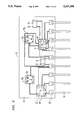
- FIG. 1 contains an exploded view of an exemplary optoelectronic circuit with a single in-line package (SIP) pinout, showing the location of various electrical and optical components with respect to the silicon substrate;
- SIP single in-line package
- FIG. 2 illustrates an exemplary silicon substrate utilized in a SIP of the present invention, showing in particular the various bond pad site locations;
- FIG. 3 contains a top view of an exemplary substrate, subsequent to metallization and placement of integrated circuits and active optical devices;
- FIG. 4 is a cut-away side view of the arrangement of FIG. 3;
- FIG. 5 illustrates an exemplary lens holder suitable for utilization with the arrangement of FIG. 1;
- FIG. 6 contains a top view of an exemplary transceiver SIP after attachment of the lens holder of FIG. 5;
- FIG. 7 illustrates an exemplary lens holder and lens suitable for utilization with the arrangement of FIG. 1;
- FIG. 8 is a cut-away side view of an exemplary transceiver SIP after attachment of the lens as shown in FIG. 7;
- FIG. 9 is a top view of the arrangement of FIG. 8;
- FIG. 10 is a cut-away side view of an exemplary transceiver SIP after the attachment of a pair of optical fiber ferrule receptacles;
- FIG. 11 is a top view of the arrangement of FIG. 10;
- FIG. 12 is a cut-away side view of an exemplary transceiver SIP after the overmolded outer package is formed
- FIG. 13 contains a perspective view of an exemplary SIP package subsequent to molding
- FIG. 14 contains a view of an exemplary SIP transceiver, including a two-piece, clam-shell outer package.
- FIG. 1 illustrates, in an exploded view, an exemplary partially processed optical assembly 10 based upon a silicon substrate 12, showing a number of the electrical and optical components which are used to populate substrate 12 and form an optical transceiver. It is to be noted that while the following discussion will focus on the assembly of an exemplary transceiver structure, the techniques of the present invention are suitable to various optical package arrangements including, but not limited to, packages for single optical devices (transmitters or receivers) or, alternatively, packages for an array of optical devices and associated electronics. Referring back to FIG.
- assembly 10 includes a silicon substrate 12 (processed to include a dielectric (e.g., SiO 2 ) surface) which has been metallized (using a conventional metallization such as gold, or a tri-layer structure of Ti-Pt-Au), the metallization pattern defined by standard photolithographic procedures well-known in the silicon processing art. As shown, the metallization is formed to provide a plurality of bond pad sites 14 along one edge of the top surface 13 of substrate 12, bond pad sites 14 being used to provide for the attachment of a plurality of leads 16 from a leadframe. Various metallized paths (clearly illustrated in the following FIG. 2) are also patterned and formed during the metallization process and utilized as discussed in detail below to interconnect the various electrical and optical components.
- a dielectric e.g., SiO 2
- metallization pattern defined by standard photolithographic procedures well-known in the silicon processing art.
- the metallization is formed to provide a plurality of bond pad sites 14 along one edge of the top surface 13 of substrate
- a transmitter circuit 18 and receiver circuit 20 are shown as positioned on top surface 13 of substrate 12.
- circuits 18 and 20 are attached utilizing "flip-chip" technology, which removes the need for any wire bond attachments (reducing capacitance problems and improving thermal dissipation).
- a de-coupling capacitor 22 for electrically isolating transmitter circuit 18 from receiver circuit 20
- bypass capacitor 24 associated with the responsivity of receiver circuit 20
- passive components may be formed directly on the silicon substrate.
- An advantage of the utilization of a silicon substrate is the ability of silicon to transport the heat generated by circuits 18 and 20 away from the heat-generating optical devices.
- the utilization of silicon as the substrate material also serves to spread the heat in a uniform manner, when compared to the thermal transport properties of a copper leadframe, as used with some prior art optical packages.
- the utilization of silicon allows for a better match (in terms of thermal expansion) with the electronic circuits (silicon-based) and with the optical devices to be described below.
- an optical transmitting device 26 for example, an LED
- an optical receiving device 28 for example, a photodiode
- the location of these optical devices 26, 28 with respect to substrate 12 may be controlled through well-known solder bump self-alignment techniques.
- FIG. 2 illustrates, in a top view, substrate 12 after the processing to provide the desired metallizations.
- the plurality of bond pads 14 are formed along one edge of top surface 13 of substrate 12.
- a plurality of bond pad sites 17 which will provide the necessary electrical contacts (i.e., power and data) to the underside of transmitter 18 (not shown in this view).
- a plurality of bond pad sites 19 provide the necessary underside electrical contacts to receiver circuit 20.
- the use of underside contacts (referred to as "flip-chip” bonding) thus removes the necessity to perform wirebonding operations in assembling the package of the present invention.
- the metallic lead lines (not numbered) and bond pad sites utilized to couple the optical devices (not shown) to the electrical devices are also illustrated in this view.
- FIG. 3 illustrates, in a top view, an exemplary substrate 12 after attachment of the various components discussed above.
- the bond pad sites discussed above in FIG. 2 are illustrated in phantom in FIG. 3.
- a suitable bonding material such as Au/Sn
- the components are then placed on substrate 12 (using a conventional pick-and-place tool, for example).
- Substrate 12 is then heated to a temperature sufficient to melt the bonding material, which subsequently liquifies (i.e., re-flows).
- an additional benefit of utilizing silicon is the ability to etch the material to form any desired number and pattern of alignment fiducials.
- the formation of such alignment fiducials may occur before or after metallization and is of no concern in practicing the techniques of the present invention.
- a plurality of alignment fiducials, denoted 30 and 32 may be etched in top surface 13 of substrate 12 in the vicinity of optical devices 26 and 28, respectively.
- Alignment fiducials 30, 32 are used, as described in detail below, to provide alignment of the remaining optical components (lens, fiber ferrule receptacle) to active devices 26 and 28.
- FIG. 4 contains a cut-away side view of the arrangement of FIG. 3, illustrating in particular the location of leads 16 and the formation of fiducials 30, 32 in top surface 13 of silicon substrate 12. The location of optical devices 26 and 28 is also shown in this view. Not evident in this particular view are electronic circuits 18 and 20, or capacitors 22 and 24, which are omitted only for the sake of clarity.
- FIG. 5 illustrates an exemplary lens holder 34 which may be utilized in the assembly of an exemplary SIP arrangement of the present invention.
- lens holder 34 comprises a silicon piece part.
- lens holder 34 contains a plurality of alignment fiducials 36 which correspond to a like number of alignment fiducials (either 30 or 32) formed on surface 13 of substrate 12.
- FIG. 6 contains a top view of an exemplary SIP assembly including a pair of lens holders 34 1 and 34 2 attached to top surface 13 of substrate 12 by mating of associated fiducials 36 1 to 30 and 36 2 to 32. The locations of active devices 26 and 28 is clearly visible through apertures 40 formed in lens holders 34.
- FIG. 8 illustrates a cut-away side view of the exemplary assembly of FIG. 6 (without the associated electrical components) including a pair of lenses 42 1 and 42 2 supported by the associated lens holders 34 1 and 34 2 , respectively.
- FIG. 7 contains a top view of an exemplary SIP assembly, including lenses 42 supported by lens holders 34.
- FIG. 10 contains a cut-away side view of an exemplary arrangement with ferrule receptacle 50 positioned over active device 26 and lens 42 1 and ferrule receptacle 52 positioned over active device 28 and lens 42 2 .
- Each ferrule receptacle includes an axial bore 54 for later placement of an optical fiber ferrule (which includes the optical fiber).
- a narrowed region 56 of bore 54 functions as a mechanical stop for the fiber ferrule, as well as to capture the associated lens 42, which aligns the ferrule receptacle to the lens and, therefore, to the underlying optics (see Ser. No. 926,555, filed Aug. 6, 1992, entitled “Optical Fiber Ferrule Assembly” and assigned to the assignee of the present application for a thorough discussion of fiber ferrule alignment).
- An alignment flange 58 is formed to surround each ferrule receptacle 50, 52, as shown in FIG. 10. As will be described hereinbelow, flange 58 is utilized to align a connector assembly to each ferrule receptacle 50, 52.
- FIG. 11 contains a top view of an exemplary SIP assembly with mounted ferrule receptacles 50, 52.
- Ferrule receptacles 50, 52 may be attached to surface 13 of substrate 12 by providing metallized surfaces which can be heat treated to provide attachment.
- temporary attachment (tacking) of ferrule receptacles 50, 52 to substrate 12 is sufficient.
- the optical assembly described above including the lens holder, lens and ferrule receptacle is exemplary only.
- a lensed fiber may be used in place of (or in addition to) a separate coupling lens.
- the ferrule receptacle as described above may be modified to incorporate the alignment fiducials directly and support the coupling lens (if any), removing the need for a separate lens holder piece part.
- any arrangement suitable for supporting an optical fiber and providing passive alignment between the fiber and underlying active optical device is suitable for use in the arrangement of the present invention.
- FIG. 12 illustrates an exemplary SIP assembly which includes such an overmolded outer package 60.
- Package 60 may be formed of a material such as a thermoset plastic (which may be transfer molded) or a liquid crystal polymer material (which may be injection molded) to provide the final package as shown. The molding process may be accomplished such that substrate 12 and the bottom portions of ferrule receptacles 50 and 52 are completely encapsulated.
- FIG. 13 An exploded view of the final assembly is illustrated in FIG. 13, which illustrates the position of leads 16 as they exit package 60.
- connector receptacles 62, 64 may simply comprise plastic piece parts 66, 68 which fit over ferrule receptacles 50, 52, such that indented portions 65, 67 mate with flanges 58.
- package 60 may be molded so as to incorporate connector receptacles 62, 64.
- a two-piece clam-shell package may also be used, with a first piece supporting silicon substrate 12 and a second piece containing the necessary receptacles.
- the arrangement as illustrated in FIG. 14 may comprise a two-piece outer package 70 with a first shell piece 72 supporting silicon substrate 12 and a second shell piece 74 formed to include connector receptacles 62, 64.
- second shell piece 74 slides over the outer diameter of ferrule receptacles 50, 52 and mates with top surface 73 of first shell piece 72. Surface 73 is thus used as the reference surface in this embodiment.
- Shell pieces 72 and 74 may comprise metal-plated plastic piece parts (either single- or doubled-sided plating) for shielding of EMI/RFI. This metallization may also be physically contacted to a ground plane formed on surface 13 of substrate 12 by conventional means (metallic springs, for example). Shell pieces 72 and 74 may be joined together using an ultrasonic weld, or snap fit together with bayonet catches, as is well known in the art. After shell pieces 72 and 74 are joined, the populated silicon substrate 12 may be encapsulated (or potted) to provide further environmental resistance.
- the clam-shell arrangement as shown in FIG. 14 may be, in most cases, a preferred embodiment, since the molds used to manufacture clam shell piece parts 72, 74 would be less complex than the mold required to overmold the assembly as shown in FIG. 10.
- leads 16 and fiber ferrule receptacles 50, 52 and any mounting posts must be clamped in place to limit motion and confine the flow of resin.
- Receptacles 50, 52 must be clamped on their outer surfaces, thus no thermoset compound will enter their respective bores.
- an overmolded assembly as illustrated in FIGS. 10 and 12 will require corepulls/clamps in the mold as as result of the undercuts introduced by flanges 58, as well as the mounting posts.
- the self-aligning and molding techniques of the present invention are applicable to virtually any optical design, such as the packaging of a single optical device and associated electronics.
- the process maybe used to provide for the packaging of an array of optical components, such as an array of LEDs or photodiodes.
Landscapes
- Physics & Mathematics (AREA)
- General Physics & Mathematics (AREA)
- Optics & Photonics (AREA)
- Optical Couplings Of Light Guides (AREA)
Priority Applications (4)
| Application Number | Priority Date | Filing Date | Title |
|---|---|---|---|
| US07/984,062 US5337398A (en) | 1992-11-30 | 1992-11-30 | Single in-line optical package |
| EP93309234A EP0600645B1 (fr) | 1992-11-30 | 1993-11-18 | Boîtier optique singulier en ligne |
| DE69313789T DE69313789T2 (de) | 1992-11-30 | 1993-11-18 | Elektro-optischer Baustein mit linear angeordneten Komponenten |
| JP5320813A JPH06208037A (ja) | 1992-11-30 | 1993-11-29 | 光学パッケージ |
Applications Claiming Priority (1)
| Application Number | Priority Date | Filing Date | Title |
|---|---|---|---|
| US07/984,062 US5337398A (en) | 1992-11-30 | 1992-11-30 | Single in-line optical package |
Publications (1)
| Publication Number | Publication Date |
|---|---|
| US5337398A true US5337398A (en) | 1994-08-09 |
Family
ID=25530270
Family Applications (1)
| Application Number | Title | Priority Date | Filing Date |
|---|---|---|---|
| US07/984,062 Expired - Lifetime US5337398A (en) | 1992-11-30 | 1992-11-30 | Single in-line optical package |
Country Status (4)
| Country | Link |
|---|---|
| US (1) | US5337398A (fr) |
| EP (1) | EP0600645B1 (fr) |
| JP (1) | JPH06208037A (fr) |
| DE (1) | DE69313789T2 (fr) |
Cited By (114)
| Publication number | Priority date | Publication date | Assignee | Title |
|---|---|---|---|---|
| US5420954A (en) * | 1993-05-24 | 1995-05-30 | Photonics Research Incorporated | Parallel optical interconnect |
| US5472886A (en) * | 1994-12-27 | 1995-12-05 | At&T Corp. | Structure of and method for manufacturing an LED |
| US5546281A (en) * | 1995-01-13 | 1996-08-13 | Methode Electronics, Inc. | Removable optoelectronic transceiver module with potting box |
| US5757998A (en) * | 1996-10-02 | 1998-05-26 | International Business Machines Corporation | Multigigabit adaptable transceiver module |
| US5771218A (en) * | 1996-09-27 | 1998-06-23 | Digital Optics Corporation | Passively aligned integrated optical head including light source, detector, and optical element and methods of forming same |
| US5812717A (en) * | 1996-01-18 | 1998-09-22 | Methode Electronics, Inc. | Optical package with alignment means and method of assembling an optical package |
| US5879173A (en) * | 1995-01-13 | 1999-03-09 | Methode Electronics, Inc. | Removable transceiver module and receptacle |
| US5886971A (en) * | 1996-09-27 | 1999-03-23 | Digital Optics Corporation | Optical head structures including support substrates adjacent transparent substrates and related methods |
| US5896481A (en) * | 1997-05-30 | 1999-04-20 | The Boeing Company | Optical subassembly with a groove for aligning an optical device with an optical fiber |
| US5912872A (en) * | 1996-09-27 | 1999-06-15 | Digital Optics Corporation | Integrated optical apparatus providing separated beams on a detector and associated methods |
| US5933551A (en) * | 1995-09-29 | 1999-08-03 | The Whitaker Corp. | Bidirectional link submodule with holographic beamsplitter |
| US5940564A (en) * | 1997-08-05 | 1999-08-17 | Picolight, Inc. | Device for coupling a light source or receiver to an optical waveguide |
| US6113283A (en) * | 1997-05-15 | 2000-09-05 | Telefonaktiebolaget Lm Ericsson | Optical capsule having a connector |
| US6179627B1 (en) | 1998-04-22 | 2001-01-30 | Stratos Lightwave, Inc. | High speed interface converter module |
| US6201704B1 (en) | 1995-01-13 | 2001-03-13 | Stratos Lightwave, Inc. | Transceive module with EMI shielding |
| US6203333B1 (en) | 1998-04-22 | 2001-03-20 | Stratos Lightwave, Inc. | High speed interface converter module |
| US6213651B1 (en) | 1999-05-26 | 2001-04-10 | E20 Communications, Inc. | Method and apparatus for vertical board construction of fiber optic transmitters, receivers and transceivers |
| US6220873B1 (en) | 1999-08-10 | 2001-04-24 | Stratos Lightwave, Inc. | Modified contact traces for interface converter |
| US6220878B1 (en) | 1995-10-04 | 2001-04-24 | Methode Electronics, Inc. | Optoelectronic module with grounding means |
| US6243508B1 (en) | 1999-06-01 | 2001-06-05 | Picolight Incorporated | Electro-opto-mechanical assembly for coupling a light source or receiver to an optical waveguide |
| US20010030789A1 (en) * | 1999-05-27 | 2001-10-18 | Wenbin Jiang | Method and apparatus for fiber optic modules |
| US20010048793A1 (en) * | 1999-05-27 | 2001-12-06 | Edwin Dair | Method and apparatus for multiboard fiber optic modules and fiber optic module arrays |
| US6328482B1 (en) | 1998-06-08 | 2001-12-11 | Benjamin Bin Jian | Multilayer optical fiber coupler |
| US20020003705A1 (en) * | 2000-07-07 | 2002-01-10 | Hiroyuki Tanaka | Method of producing an optical module |
| US20020028048A1 (en) * | 1999-05-27 | 2002-03-07 | Edwin Dair | Method and apparatus for multiboard fiber optic modules and fiber optic module arrays |
| US20020030872A1 (en) * | 1999-05-27 | 2002-03-14 | Edwin Dair | Method and apparatus for multiboard fiber optic modules and fiber optic module arrays |
| US20020033979A1 (en) * | 1999-05-27 | 2002-03-21 | Edwin Dair | Method and apparatus for multiboard fiber optic modules and fiber optic module arrays |
| US20020084565A1 (en) * | 2000-08-07 | 2002-07-04 | Dautartas Mindaugas F. | Alignment apparatus and method for aligning stacked devices |
| US20020104822A1 (en) * | 2001-02-02 | 2002-08-08 | Naydenkov Mikhail N. | Method of providing optical quality silicon surface |
| US6453081B1 (en) * | 1999-10-22 | 2002-09-17 | Teraconnect, Inc. | Optoelectronic device with integrated passive optical elements and method |
| US6453091B2 (en) * | 1999-01-12 | 2002-09-17 | Nec Corporation | Optical system unit for optical transceiver |
| US20020196996A1 (en) * | 2001-06-20 | 2002-12-26 | International Business Machines Corporation | Interconnect structure and process for silicon optical bench |
| US20030034438A1 (en) * | 1998-11-25 | 2003-02-20 | Sherrer David W. | Optoelectronic device-optical fiber connector having micromachined pit for passive alignment of the optoelectronic device |
| US20030044118A1 (en) * | 2000-10-20 | 2003-03-06 | Phosistor Technologies, Inc. | Integrated planar composite coupling structures for bi-directional light beam transformation between a small mode size waveguide and a large mode size waveguide |
| EP1304543A1 (fr) * | 2001-10-22 | 2003-04-23 | Agilent Technologies, Inc. (a Delaware corporation) | Positionnement par des marques conductrices ( silicon optical bench ) |
| US20030095758A1 (en) * | 2001-11-20 | 2003-05-22 | Harris Corporation | Optical connector adapter for interfacing single or multichannel waveguide devices to fiber and method of forming same |
| US20030161591A1 (en) * | 2002-02-26 | 2003-08-28 | Shin-Terng Chiang | Passive alignment packaging structure for opto-electrical devices and optic fiber connectors |
| US6614949B2 (en) * | 2000-04-21 | 2003-09-02 | Teraconnect, Inc. | Precision grid standoff for optical components on opto-electronic devices |
| US6627096B2 (en) | 2000-05-02 | 2003-09-30 | Shipley Company, L.L.C. | Single mask technique for making positive and negative micromachined features on a substrate |
| US6632030B2 (en) | 1999-05-27 | 2003-10-14 | E20 Communications, Inc. | Light bending optical block for fiber optic modules |
| US6634802B2 (en) | 2001-08-09 | 2003-10-21 | International Business Machines Corporation | Optical-electronic array module and method therefore |
| US20030210866A1 (en) * | 2002-05-10 | 2003-11-13 | Yoshiki Kuhara | Optical transceiver module and optical communications system using the same |
| WO2003104850A3 (fr) * | 2002-06-06 | 2004-02-26 | E20 Communications Inc | Systemes, procedes et appareil pour emetteurs-recepteurs optiques bidirectionnels |
| US20040042729A1 (en) * | 2002-08-28 | 2004-03-04 | Phosistor Technologies, Inc. | Optical beam transformer module for light coupling between a fiber array and a photonic chip and the method of making the same |
| US20040069997A1 (en) * | 1999-05-27 | 2004-04-15 | Edwin Dair | Method and apparatus for multiboard fiber optic modules and fiber optic module arrays |
| US6741778B1 (en) | 2000-05-23 | 2004-05-25 | International Business Machines Corporation | Optical device with chip level precision alignment |
| US20040100781A1 (en) * | 2002-11-27 | 2004-05-27 | Bozso Ferenc M. | Optically connectable circuit board with optical component(s) mounted thereon |
| US6742938B2 (en) * | 2000-07-25 | 2004-06-01 | Nippon Sheet Glass Co., Ltd. | Optical module for coupling an optical semiconductor element having a sealing cap with an optical fiber |
| US20040105628A1 (en) * | 2001-11-20 | 2004-06-03 | Harris Corporation | Optical connector adapter for connecting optical pump sources to optical waveguides and method of forming same |
| US20040182838A1 (en) * | 2001-04-18 | 2004-09-23 | Das Palash P. | Very high energy, high stability gas discharge laser surface treatment system |
| KR100450821B1 (ko) * | 2002-05-29 | 2004-10-01 | 삼성전자주식회사 | Mems를 이용한 광학 소자의 제조방법 |
| US6799902B2 (en) | 2000-12-26 | 2004-10-05 | Emcore Corporation | Optoelectronic mounting structure |
| US6811853B1 (en) | 2000-03-06 | 2004-11-02 | Shipley Company, L.L.C. | Single mask lithographic process for patterning multiple types of surface features |
| US20050030722A1 (en) * | 2003-08-07 | 2005-02-10 | John Bohlin | Bulkhead mountable optoelectronic device |
| US20050036738A1 (en) * | 2002-08-28 | 2005-02-17 | Phosistor Technologies, Inc. | Varying refractive index optical medium using at least two materials with thicknesses less than a wavelength |
| US6863453B2 (en) | 2003-01-28 | 2005-03-08 | Emcore Corporation | Method and apparatus for parallel optical transceiver module assembly |
| US6863444B2 (en) | 2000-12-26 | 2005-03-08 | Emcore Corporation | Housing and mounting structure |
| US6867377B2 (en) | 2000-12-26 | 2005-03-15 | Emcore Corporation | Apparatus and method of using flexible printed circuit board in optical transceiver device |
| US6873800B1 (en) | 1999-05-26 | 2005-03-29 | Jds Uniphase Corporation | Hot pluggable optical transceiver in a small form pluggable package |
| US6879757B1 (en) | 2001-12-11 | 2005-04-12 | Phosistor Technologies, Inc. | Connection between a waveguide array and a fiber array |
| US6888989B1 (en) | 2001-12-11 | 2005-05-03 | Phosistor Technologies, Inc. | Photonic chip mounting in a recess for waveguide alignment and connection |
| WO2005045499A1 (fr) * | 2003-11-10 | 2005-05-19 | Melexis Nv | Transmission optique de donnees, emetteurs-recepteurs optiques de donnees et leur procede de fabrication et de mise sous boitier |
| US20050105910A1 (en) * | 2003-11-17 | 2005-05-19 | Greta Light | Optical transceiver with integrated feedback device |
| US20050105915A1 (en) * | 2003-11-17 | 2005-05-19 | Greta Light | Compact optical transceivers for host bus adapters |
| US6901221B1 (en) | 1999-05-27 | 2005-05-31 | Jds Uniphase Corporation | Method and apparatus for improved optical elements for vertical PCB fiber optic modules |
| US20050123246A1 (en) * | 2001-11-20 | 2005-06-09 | Harris Corporation | Optical connector adapter for interfacing a beam splitter/combiner to optical waveguides and method of forming the same |
| US6905260B2 (en) | 2000-12-26 | 2005-06-14 | Emcore Corporation | Method and apparatus for coupling optical elements to optoelectronic devices for manufacturing optical transceiver modules |
| US20050180700A1 (en) * | 2003-12-12 | 2005-08-18 | Finisar Corporation | Optical connectors for electronic devices |
| US20050226565A1 (en) * | 2002-06-24 | 2005-10-13 | Kari Kautio | Alignment of an optic or electronic component |
| US20050238358A1 (en) * | 2004-04-22 | 2005-10-27 | Greta Light | Compact optical transceivers |
| US20050263841A1 (en) * | 2004-05-31 | 2005-12-01 | Stmicroelectronics S.R.L. | Package for housing at least an electro-optic active element, electro-optic and assembling method |
| US7013088B1 (en) | 1999-05-26 | 2006-03-14 | Jds Uniphase Corporation | Method and apparatus for parallel optical interconnection of fiber optic transmitters, receivers and transceivers |
| US7021836B2 (en) | 2000-12-26 | 2006-04-04 | Emcore Corporation | Attenuator and conditioner |
| US20060153507A1 (en) * | 2004-05-21 | 2006-07-13 | Togami Chris K | Modular optical devices compatible with legacy form factors |
| US7090509B1 (en) | 1999-06-11 | 2006-08-15 | Stratos International, Inc. | Multi-port pluggable transceiver (MPPT) with multiple LC duplex optical receptacles |
| US7116912B2 (en) | 1999-05-27 | 2006-10-03 | Jds Uniphase Corporation | Method and apparatus for pluggable fiber optic modules |
| WO2006103512A1 (fr) * | 2005-03-29 | 2006-10-05 | Melexis Nv | Emetteur-recepteur de donnees optiques |
| US20060289975A1 (en) * | 2005-06-22 | 2006-12-28 | Jose Joaquin Aizpuru | Alignment using fiducial features |
| US20070010132A1 (en) * | 2005-07-11 | 2007-01-11 | Finisar Corporation | Media converter |
| US20070058976A1 (en) * | 2005-09-15 | 2007-03-15 | Tatum Jimmy A | Laser drivers for closed path optical cables |
| US20070110361A1 (en) * | 2003-08-26 | 2007-05-17 | Digital Optics Corporation | Wafer level integration of multiple optical elements |
| US7268368B1 (en) | 2003-08-29 | 2007-09-11 | Standard Microsystems Corporation | Semiconductor package having optical receptacles and light transmissive/opaque portions and method of making same |
| US20070237462A1 (en) * | 2006-04-10 | 2007-10-11 | Aronson Lewis B | Active optical cable with integrated power |
| US20070237470A1 (en) * | 2006-04-10 | 2007-10-11 | Aronson Lewis B | Active optical cable with electrical connector |
| US20070237472A1 (en) * | 2006-04-10 | 2007-10-11 | Aronson Lewis B | Active optical cable electrical connector |
| US20070237463A1 (en) * | 2006-04-10 | 2007-10-11 | Aronson Lewis B | Active optical cable with integrated eye safety |
| US20070237464A1 (en) * | 2006-04-10 | 2007-10-11 | Aronson Lewis B | Electrical-optical active optical cable |
| US20070237468A1 (en) * | 2006-04-10 | 2007-10-11 | Aronson Lewis B | Active optical cable electrical adaptor |
| US20070258680A1 (en) * | 2006-05-05 | 2007-11-08 | Sioptical, Inc. | Passive fiber alignment arrangement for coupling to nano-taper optical waveguides |
| US20070267569A1 (en) * | 2006-05-17 | 2007-11-22 | Fuji Xerox Co., Ltd. | Optical transmission module and method of manufacturing the same |
| JP2007534988A (ja) * | 2004-04-28 | 2007-11-29 | フィニサー コーポレイション | モジュラー光デバイス・パッケージ |
| USRE40150E1 (en) | 1994-04-25 | 2008-03-11 | Matsushita Electric Industrial Co., Ltd. | Fiber optic module |
| US20080111058A1 (en) * | 1996-09-27 | 2008-05-15 | Tessera North America | Integrated optical systems and associated methods |
| US20080136955A1 (en) * | 1996-09-27 | 2008-06-12 | Tessera North America. | Integrated camera and associated methods |
| US20080224287A1 (en) * | 2007-03-16 | 2008-09-18 | Finisar Corporation | Optoelectronic device alignment in an optoelectronic package |
| US20090103850A1 (en) * | 2007-10-19 | 2009-04-23 | Lightwire, Inc. | Silicon-based optical modulator for analog applications |
| US7548675B2 (en) | 2004-09-29 | 2009-06-16 | Finisar Corporation | Optical cables for consumer electronics |
| US20090245735A1 (en) * | 2008-04-01 | 2009-10-01 | General Electric Company | Photonic power devices and methods of manufacturing the same |
| US20100046955A1 (en) * | 2005-12-14 | 2010-02-25 | Peter De Dobbelaere | Integrated transceiver with lightpipe coupler |
| US7706692B2 (en) | 2004-09-29 | 2010-04-27 | Finisar Corporation | Consumer electronics with optical communication interface |
| US7712976B2 (en) | 2006-04-10 | 2010-05-11 | Finisar Corporation | Active optical cable with integrated retiming |
| US7729618B2 (en) | 2005-08-30 | 2010-06-01 | Finisar Corporation | Optical networks for consumer electronics |
| US20100135615A1 (en) * | 2002-08-28 | 2010-06-03 | Seng-Tiong Ho | Apparatus for coupling light between input and output waveguides |
| US7731433B1 (en) | 2008-12-05 | 2010-06-08 | Avago Technologies Fiber Ip (Singapore) Pte. Ltd. | Optoelectronic surface-mounted device and method for forming an optoelectronic surface-mounted device |
| US7805084B2 (en) | 2004-05-20 | 2010-09-28 | Finisar Corporation | Dual stage modular optical devices |
| US20100325324A1 (en) * | 2007-04-06 | 2010-12-23 | Finisar Corporation | Electrical device with electrical interface that is compatible with optical cables |
| US8244124B2 (en) | 2007-04-30 | 2012-08-14 | Finisar Corporation | Eye safety mechanism for use in optical cable with electrical interfaces |
| US20130302040A1 (en) * | 2012-05-14 | 2013-11-14 | Kuo-Fong Tseng | Optical-electrical conversion module and optical transmission assembly using the same |
| US20140254985A1 (en) * | 2013-03-06 | 2014-09-11 | Hon Hai Precision Industry Co., Ltd. | Optical connector and method for assembling same |
| US8834041B2 (en) | 2011-09-29 | 2014-09-16 | Corning Cable Systems Llc | Ferrule-based optical component assemblies |
| US20140286612A1 (en) * | 2013-03-20 | 2014-09-25 | All Best Precision Technology Co., Ltd. | Coupling device |
| US9170387B2 (en) | 2011-09-29 | 2015-10-27 | Corning Cable Systems Llc | Optical component assemblies |
| US20230280552A1 (en) * | 2020-09-09 | 2023-09-07 | HARTING Electronics GmbH | Optoelectronic module, optoelectronic plug connector and optoelectronic sub-distribution unit |
| CN117242384A (zh) * | 2021-05-03 | 2023-12-15 | 3M创新有限公司 | 具有对准特征结构的光子集成电路封装 |
Families Citing this family (12)
| Publication number | Priority date | Publication date | Assignee | Title |
|---|---|---|---|---|
| US5535296A (en) * | 1994-09-28 | 1996-07-09 | Optobahn Corporation | Integrated optoelectronic coupling and connector |
| US5528408A (en) * | 1994-10-12 | 1996-06-18 | Methode Electronics, Inc. | Small footprint optoelectronic transceiver with laser |
| SE516160C2 (sv) | 1995-04-28 | 2001-11-26 | Ericsson Telefon Ab L M | Kapslad optoelektronisk komponent |
| US6014476A (en) | 1996-05-24 | 2000-01-11 | Siemens Aktiengesellschaft | Electro-optical module |
| DE19622459C1 (de) * | 1996-05-24 | 1997-11-27 | Siemens Ag | Elektrooptisches Modul |
| JPH1123914A (ja) * | 1997-07-02 | 1999-01-29 | Nec Corp | 光素子と光ファイバとの固定構造 |
| DE19755806A1 (de) * | 1997-12-16 | 1999-06-17 | Bosch Gmbh Robert | Elektrooptisches Modul |
| EP1180703A1 (fr) * | 2000-08-11 | 2002-02-20 | Delphi Technologies, Inc. | Module opto-électronique avec support à ressort pour transmetteur et récepteur optiques |
| GB2387923B (en) * | 2001-02-20 | 2004-06-02 | Cyberoptics Corp | Optical device |
| US6546173B2 (en) | 2001-02-20 | 2003-04-08 | Avanti Optics Corporation | Optical module |
| US6546172B2 (en) | 2001-02-20 | 2003-04-08 | Avanti Optics Corporation | Optical device |
| US20040212802A1 (en) | 2001-02-20 | 2004-10-28 | Case Steven K. | Optical device with alignment compensation |
Citations (18)
| Publication number | Priority date | Publication date | Assignee | Title |
|---|---|---|---|---|
| US4410469A (en) * | 1980-11-28 | 1983-10-18 | Tokyo Shibaura Denki Kabushiki Kaisha | Method for manufacturing a module for a fiber optic link |
| US4427879A (en) * | 1975-04-18 | 1984-01-24 | Allied Corporation | Optoelectronic connector assembly |
| US4539476A (en) * | 1980-11-28 | 1985-09-03 | Tokyo Shibaura Denki Kabushiki Kaisha | Module for a fiber optic link |
| US4625333A (en) * | 1982-10-26 | 1986-11-25 | Tokyo Shibaura Denki Kabushiki Kaisha | Duplex optical communication device |
| US4647148A (en) * | 1983-03-31 | 1987-03-03 | Tokyo Shibaura Denki Kabushiki Kaisha | Fiber optic receiver module |
| US4897711A (en) * | 1988-03-03 | 1990-01-30 | American Telephone And Telegraph Company | Subassembly for optoelectronic devices |
| US4911519A (en) * | 1989-02-01 | 1990-03-27 | At&T Bell Laboratories | Packaging techniques for optical transmitters/receivers |
| US4933729A (en) * | 1985-11-21 | 1990-06-12 | Nec Corporation | Photointerrupter |
| US5061033A (en) * | 1990-12-03 | 1991-10-29 | Motorola, Inc. | Removable optical interconnect for electronic modules |
| US5113466A (en) * | 1991-04-25 | 1992-05-12 | At&T Bell Laboratories | Molded optical packaging arrangement |
| US5123066A (en) * | 1991-04-25 | 1992-06-16 | At&T Bell Laboratories | Molded optical package utilizing leadframe technology |
| US5163108A (en) * | 1990-07-11 | 1992-11-10 | Gte Laboratories Incorporated | Method and device for passive alignment of diode lasers and optical fibers |
| US5179609A (en) * | 1991-08-30 | 1993-01-12 | At&T Bell Laboratories | Optical assembly including fiber attachment |
| US5182782A (en) * | 1990-07-11 | 1993-01-26 | Gte Laboratories Incorporated | Waferboard structure and method of fabricating |
| US5222175A (en) * | 1991-07-09 | 1993-06-22 | Sumitomo Electric Industries, Ltd. | Optical integrated light receiving apparatus |
| US5249245A (en) * | 1992-08-31 | 1993-09-28 | Motorola, Inc. | Optoelectroinc mount including flexible substrate and method for making same |
| US5257336A (en) * | 1992-08-21 | 1993-10-26 | At&T Bell Laboratories | Optical subassembly with passive optical alignment |
| US5259054A (en) * | 1992-01-10 | 1993-11-02 | At&T Bell Laboratories | Self-aligned optical subassembly |
Family Cites Families (4)
| Publication number | Priority date | Publication date | Assignee | Title |
|---|---|---|---|---|
| JPS59101882A (ja) * | 1982-12-03 | 1984-06-12 | Nec Corp | 光半導体装置 |
| US4826272A (en) * | 1987-08-27 | 1989-05-02 | American Telephone And Telegraph Company At&T Bell Laboratories | Means for coupling an optical fiber to an opto-electronic device |
| JPH03141308A (ja) * | 1989-07-17 | 1991-06-17 | Nippon Telegr & Teleph Corp <Ntt> | 受光モジュールおよびその製造方法 |
| US4995695A (en) * | 1989-08-17 | 1991-02-26 | At&T Bell Laboratories | Optical assembly comprising optical fiber coupling means |
-
1992
- 1992-11-30 US US07/984,062 patent/US5337398A/en not_active Expired - Lifetime
-
1993
- 1993-11-18 EP EP93309234A patent/EP0600645B1/fr not_active Expired - Lifetime
- 1993-11-18 DE DE69313789T patent/DE69313789T2/de not_active Expired - Fee Related
- 1993-11-29 JP JP5320813A patent/JPH06208037A/ja active Pending
Patent Citations (18)
| Publication number | Priority date | Publication date | Assignee | Title |
|---|---|---|---|---|
| US4427879A (en) * | 1975-04-18 | 1984-01-24 | Allied Corporation | Optoelectronic connector assembly |
| US4539476A (en) * | 1980-11-28 | 1985-09-03 | Tokyo Shibaura Denki Kabushiki Kaisha | Module for a fiber optic link |
| US4410469A (en) * | 1980-11-28 | 1983-10-18 | Tokyo Shibaura Denki Kabushiki Kaisha | Method for manufacturing a module for a fiber optic link |
| US4625333A (en) * | 1982-10-26 | 1986-11-25 | Tokyo Shibaura Denki Kabushiki Kaisha | Duplex optical communication device |
| US4647148A (en) * | 1983-03-31 | 1987-03-03 | Tokyo Shibaura Denki Kabushiki Kaisha | Fiber optic receiver module |
| US4933729A (en) * | 1985-11-21 | 1990-06-12 | Nec Corporation | Photointerrupter |
| US4897711A (en) * | 1988-03-03 | 1990-01-30 | American Telephone And Telegraph Company | Subassembly for optoelectronic devices |
| US4911519A (en) * | 1989-02-01 | 1990-03-27 | At&T Bell Laboratories | Packaging techniques for optical transmitters/receivers |
| US5163108A (en) * | 1990-07-11 | 1992-11-10 | Gte Laboratories Incorporated | Method and device for passive alignment of diode lasers and optical fibers |
| US5182782A (en) * | 1990-07-11 | 1993-01-26 | Gte Laboratories Incorporated | Waferboard structure and method of fabricating |
| US5061033A (en) * | 1990-12-03 | 1991-10-29 | Motorola, Inc. | Removable optical interconnect for electronic modules |
| US5123066A (en) * | 1991-04-25 | 1992-06-16 | At&T Bell Laboratories | Molded optical package utilizing leadframe technology |
| US5113466A (en) * | 1991-04-25 | 1992-05-12 | At&T Bell Laboratories | Molded optical packaging arrangement |
| US5222175A (en) * | 1991-07-09 | 1993-06-22 | Sumitomo Electric Industries, Ltd. | Optical integrated light receiving apparatus |
| US5179609A (en) * | 1991-08-30 | 1993-01-12 | At&T Bell Laboratories | Optical assembly including fiber attachment |
| US5259054A (en) * | 1992-01-10 | 1993-11-02 | At&T Bell Laboratories | Self-aligned optical subassembly |
| US5257336A (en) * | 1992-08-21 | 1993-10-26 | At&T Bell Laboratories | Optical subassembly with passive optical alignment |
| US5249245A (en) * | 1992-08-31 | 1993-09-28 | Motorola, Inc. | Optoelectroinc mount including flexible substrate and method for making same |
Cited By (204)
| Publication number | Priority date | Publication date | Assignee | Title |
|---|---|---|---|---|
| US5631988A (en) * | 1993-05-24 | 1997-05-20 | Vixel Corporation | Parallel optical interconnect |
| US5420954A (en) * | 1993-05-24 | 1995-05-30 | Photonics Research Incorporated | Parallel optical interconnect |
| USRE40154E1 (en) | 1994-04-25 | 2008-03-18 | Matsushita Electric Industrial Co., Ltd. | Fiber optic module |
| USRE40150E1 (en) | 1994-04-25 | 2008-03-11 | Matsushita Electric Industrial Co., Ltd. | Fiber optic module |
| US5472886A (en) * | 1994-12-27 | 1995-12-05 | At&T Corp. | Structure of and method for manufacturing an LED |
| US6267606B1 (en) * | 1995-01-13 | 2001-07-31 | Stratos Lightwave, Inc. | Removable transceiver module and receptacle |
| US5546281A (en) * | 1995-01-13 | 1996-08-13 | Methode Electronics, Inc. | Removable optoelectronic transceiver module with potting box |
| US5879173A (en) * | 1995-01-13 | 1999-03-09 | Methode Electronics, Inc. | Removable transceiver module and receptacle |
| USRE36820E (en) | 1995-01-13 | 2000-08-15 | Methode Electronics, Inc. | Removable optoelectronic module |
| US6201704B1 (en) | 1995-01-13 | 2001-03-13 | Stratos Lightwave, Inc. | Transceive module with EMI shielding |
| US5933551A (en) * | 1995-09-29 | 1999-08-03 | The Whitaker Corp. | Bidirectional link submodule with holographic beamsplitter |
| US6220878B1 (en) | 1995-10-04 | 2001-04-24 | Methode Electronics, Inc. | Optoelectronic module with grounding means |
| US5812717A (en) * | 1996-01-18 | 1998-09-22 | Methode Electronics, Inc. | Optical package with alignment means and method of assembling an optical package |
| US5886971A (en) * | 1996-09-27 | 1999-03-23 | Digital Optics Corporation | Optical head structures including support substrates adjacent transparent substrates and related methods |
| US20080136955A1 (en) * | 1996-09-27 | 2008-06-12 | Tessera North America. | Integrated camera and associated methods |
| US5771218A (en) * | 1996-09-27 | 1998-06-23 | Digital Optics Corporation | Passively aligned integrated optical head including light source, detector, and optical element and methods of forming same |
| US20080111058A1 (en) * | 1996-09-27 | 2008-05-15 | Tessera North America | Integrated optical systems and associated methods |
| US6104690A (en) * | 1996-09-27 | 2000-08-15 | Digital Optics Corporation | Integrated optical apparatus and associated methods |
| US5912872A (en) * | 1996-09-27 | 1999-06-15 | Digital Optics Corporation | Integrated optical apparatus providing separated beams on a detector and associated methods |
| US5872762A (en) * | 1996-09-27 | 1999-02-16 | Digital Optics Corporation | Optical head structures including electronic devices adjacent transparent substrates and related methods |
| US6522618B1 (en) | 1996-09-27 | 2003-02-18 | Digital Optics Corp. | Integrated optical apparatus and associated methods |
| US8153957B2 (en) | 1996-09-27 | 2012-04-10 | Digitaloptics Corporation East | Integrated optical imaging systems including an interior space between opposing substrates and associated methods |
| US5757998A (en) * | 1996-10-02 | 1998-05-26 | International Business Machines Corporation | Multigigabit adaptable transceiver module |
| US6113283A (en) * | 1997-05-15 | 2000-09-05 | Telefonaktiebolaget Lm Ericsson | Optical capsule having a connector |
| US5896481A (en) * | 1997-05-30 | 1999-04-20 | The Boeing Company | Optical subassembly with a groove for aligning an optical device with an optical fiber |
| US5940564A (en) * | 1997-08-05 | 1999-08-17 | Picolight, Inc. | Device for coupling a light source or receiver to an optical waveguide |
| US6203333B1 (en) | 1998-04-22 | 2001-03-20 | Stratos Lightwave, Inc. | High speed interface converter module |
| US6179627B1 (en) | 1998-04-22 | 2001-01-30 | Stratos Lightwave, Inc. | High speed interface converter module |
| US6527455B2 (en) | 1998-06-08 | 2003-03-04 | Benjamin B. Jian | Multilayer optical fiber coupler |
| USRE40416E1 (en) | 1998-06-08 | 2008-07-01 | Benjamin Jian | Multilayer optical fiber coupler |
| US6328482B1 (en) | 1998-06-08 | 2001-12-11 | Benjamin Bin Jian | Multilayer optical fiber coupler |
| US20030034438A1 (en) * | 1998-11-25 | 2003-02-20 | Sherrer David W. | Optoelectronic device-optical fiber connector having micromachined pit for passive alignment of the optoelectronic device |
| US6453091B2 (en) * | 1999-01-12 | 2002-09-17 | Nec Corporation | Optical system unit for optical transceiver |
| US6873800B1 (en) | 1999-05-26 | 2005-03-29 | Jds Uniphase Corporation | Hot pluggable optical transceiver in a small form pluggable package |
| US7013088B1 (en) | 1999-05-26 | 2006-03-14 | Jds Uniphase Corporation | Method and apparatus for parallel optical interconnection of fiber optic transmitters, receivers and transceivers |
| US6213651B1 (en) | 1999-05-26 | 2001-04-10 | E20 Communications, Inc. | Method and apparatus for vertical board construction of fiber optic transmitters, receivers and transceivers |
| US6840686B2 (en) | 1999-05-26 | 2005-01-11 | Jds Uniphase Corporation | Method and apparatus for vertical board construction of fiber optic transmitters, receivers and transceivers |
| US20020030872A1 (en) * | 1999-05-27 | 2002-03-14 | Edwin Dair | Method and apparatus for multiboard fiber optic modules and fiber optic module arrays |
| US6632030B2 (en) | 1999-05-27 | 2003-10-14 | E20 Communications, Inc. | Light bending optical block for fiber optic modules |
| US20010030789A1 (en) * | 1999-05-27 | 2001-10-18 | Wenbin Jiang | Method and apparatus for fiber optic modules |
| US20040069997A1 (en) * | 1999-05-27 | 2004-04-15 | Edwin Dair | Method and apparatus for multiboard fiber optic modules and fiber optic module arrays |
| US7116912B2 (en) | 1999-05-27 | 2006-10-03 | Jds Uniphase Corporation | Method and apparatus for pluggable fiber optic modules |
| USRE41147E1 (en) * | 1999-05-27 | 2010-02-23 | Jds Uniphase Corporation | Method and apparatus for pluggable fiber optic modules |
| US20020033979A1 (en) * | 1999-05-27 | 2002-03-21 | Edwin Dair | Method and apparatus for multiboard fiber optic modules and fiber optic module arrays |
| US6901221B1 (en) | 1999-05-27 | 2005-05-31 | Jds Uniphase Corporation | Method and apparatus for improved optical elements for vertical PCB fiber optic modules |
| US6952532B2 (en) | 1999-05-27 | 2005-10-04 | Jds Uniphase Corporation | Method and apparatus for multiboard fiber optic modules and fiber optic module arrays |
| US20010048793A1 (en) * | 1999-05-27 | 2001-12-06 | Edwin Dair | Method and apparatus for multiboard fiber optic modules and fiber optic module arrays |
| US20020028048A1 (en) * | 1999-05-27 | 2002-03-07 | Edwin Dair | Method and apparatus for multiboard fiber optic modules and fiber optic module arrays |
| US6931181B2 (en) | 1999-06-01 | 2005-08-16 | Picolight Incorporated | Opto-mechanical assembly |
| US20040184707A1 (en) * | 1999-06-01 | 2004-09-23 | Jewell Jack L. | Opto-mechanical assembly |
| US6542672B2 (en) | 1999-06-01 | 2003-04-01 | Picolight, Incorporated | Opto-mechanical assembly |
| US6421474B2 (en) | 1999-06-01 | 2002-07-16 | Picolight Incorporated | Electro-opto mechanical assembly for coupling a light source or reciever to an optical waveguide |
| US6741777B2 (en) | 1999-06-01 | 2004-05-25 | Picolight, Incorporated | Opto-mechanical assembly |
| US6243508B1 (en) | 1999-06-01 | 2001-06-05 | Picolight Incorporated | Electro-opto-mechanical assembly for coupling a light source or receiver to an optical waveguide |
| US7090509B1 (en) | 1999-06-11 | 2006-08-15 | Stratos International, Inc. | Multi-port pluggable transceiver (MPPT) with multiple LC duplex optical receptacles |
| US6220873B1 (en) | 1999-08-10 | 2001-04-24 | Stratos Lightwave, Inc. | Modified contact traces for interface converter |
| US6453081B1 (en) * | 1999-10-22 | 2002-09-17 | Teraconnect, Inc. | Optoelectronic device with integrated passive optical elements and method |
| US6811853B1 (en) | 2000-03-06 | 2004-11-02 | Shipley Company, L.L.C. | Single mask lithographic process for patterning multiple types of surface features |
| US6614949B2 (en) * | 2000-04-21 | 2003-09-02 | Teraconnect, Inc. | Precision grid standoff for optical components on opto-electronic devices |
| US6627096B2 (en) | 2000-05-02 | 2003-09-30 | Shipley Company, L.L.C. | Single mask technique for making positive and negative micromachined features on a substrate |
| US6741778B1 (en) | 2000-05-23 | 2004-05-25 | International Business Machines Corporation | Optical device with chip level precision alignment |
| US20020003705A1 (en) * | 2000-07-07 | 2002-01-10 | Hiroyuki Tanaka | Method of producing an optical module |
| US6812057B2 (en) | 2000-07-07 | 2004-11-02 | Nippon Sheet Glass Co., Ltd. | Method of producing an optical module |
| US6742938B2 (en) * | 2000-07-25 | 2004-06-01 | Nippon Sheet Glass Co., Ltd. | Optical module for coupling an optical semiconductor element having a sealing cap with an optical fiber |
| US7290321B2 (en) | 2000-08-07 | 2007-11-06 | Shipley Company, L.L.C. | Alignment apparatus and method for aligning stacked devices |
| US20060272149A1 (en) * | 2000-08-07 | 2006-12-07 | Shipley Company, L.L.C. | Alignment apparatus and method for aligning stacked devices |
| US20020084565A1 (en) * | 2000-08-07 | 2002-07-04 | Dautartas Mindaugas F. | Alignment apparatus and method for aligning stacked devices |
| US7086134B2 (en) * | 2000-08-07 | 2006-08-08 | Shipley Company, L.L.C. | Alignment apparatus and method for aligning stacked devices |
| US20030044118A1 (en) * | 2000-10-20 | 2003-03-06 | Phosistor Technologies, Inc. | Integrated planar composite coupling structures for bi-directional light beam transformation between a small mode size waveguide and a large mode size waveguide |
| US7021836B2 (en) | 2000-12-26 | 2006-04-04 | Emcore Corporation | Attenuator and conditioner |
| US6799902B2 (en) | 2000-12-26 | 2004-10-05 | Emcore Corporation | Optoelectronic mounting structure |
| US6863444B2 (en) | 2000-12-26 | 2005-03-08 | Emcore Corporation | Housing and mounting structure |
| US6867377B2 (en) | 2000-12-26 | 2005-03-15 | Emcore Corporation | Apparatus and method of using flexible printed circuit board in optical transceiver device |
| US6905260B2 (en) | 2000-12-26 | 2005-06-14 | Emcore Corporation | Method and apparatus for coupling optical elements to optoelectronic devices for manufacturing optical transceiver modules |
| US6890450B2 (en) | 2001-02-02 | 2005-05-10 | Intel Corporation | Method of providing optical quality silicon surface |
| US20020104822A1 (en) * | 2001-02-02 | 2002-08-08 | Naydenkov Mikhail N. | Method of providing optical quality silicon surface |
| US20040182838A1 (en) * | 2001-04-18 | 2004-09-23 | Das Palash P. | Very high energy, high stability gas discharge laser surface treatment system |
| US6762119B2 (en) * | 2001-06-20 | 2004-07-13 | International Bussiness Machines Corporation | Method of preventing solder wetting in an optical device using diffusion of Cr |
| US20020196996A1 (en) * | 2001-06-20 | 2002-12-26 | International Business Machines Corporation | Interconnect structure and process for silicon optical bench |
| US6634802B2 (en) | 2001-08-09 | 2003-10-21 | International Business Machines Corporation | Optical-electronic array module and method therefore |
| EP1304543A1 (fr) * | 2001-10-22 | 2003-04-23 | Agilent Technologies, Inc. (a Delaware corporation) | Positionnement par des marques conductrices ( silicon optical bench ) |
| US6647619B2 (en) | 2001-10-22 | 2003-11-18 | Agilent Technologies, Inc. | Positioning arrangement and method |
| US7234874B2 (en) | 2001-11-20 | 2007-06-26 | Harris Corporation | Optical connector adapter for connecting optical pump sources to optical waveguides and method of forming same |
| US7300216B2 (en) | 2001-11-20 | 2007-11-27 | Harris Corporation | Optical connector adapter for interfacing a beam splitter/combiner to optical waveguides and method of forming the same |
| US20050123246A1 (en) * | 2001-11-20 | 2005-06-09 | Harris Corporation | Optical connector adapter for interfacing a beam splitter/combiner to optical waveguides and method of forming the same |
| US20040105628A1 (en) * | 2001-11-20 | 2004-06-03 | Harris Corporation | Optical connector adapter for connecting optical pump sources to optical waveguides and method of forming same |
| US6905256B2 (en) | 2001-11-20 | 2005-06-14 | Harris Corporation | Optical connector adapter for interfacing single or multichannel waveguide devices to fiber and method of forming same |
| US20030095758A1 (en) * | 2001-11-20 | 2003-05-22 | Harris Corporation | Optical connector adapter for interfacing single or multichannel waveguide devices to fiber and method of forming same |
| US6879757B1 (en) | 2001-12-11 | 2005-04-12 | Phosistor Technologies, Inc. | Connection between a waveguide array and a fiber array |
| US6888989B1 (en) | 2001-12-11 | 2005-05-03 | Phosistor Technologies, Inc. | Photonic chip mounting in a recess for waveguide alignment and connection |
| US20040208601A1 (en) * | 2002-01-24 | 2004-10-21 | Ronson Tan | Systems, methods and apparatus for bi-directional optical transceivers |
| US6954592B2 (en) * | 2002-01-24 | 2005-10-11 | Jds Uniphase Corporation | Systems, methods and apparatus for bi-directional optical transceivers |
| US6808323B2 (en) * | 2002-02-26 | 2004-10-26 | Industrial Technology Research Institute | Passive alignment packaging structure for opto-electrical devices and optic fiber connectors |
| US20030161591A1 (en) * | 2002-02-26 | 2003-08-28 | Shin-Terng Chiang | Passive alignment packaging structure for opto-electrical devices and optic fiber connectors |
| US6748143B2 (en) * | 2002-05-10 | 2004-06-08 | Sumitomo Electric Industries, Ltd. | Optical transceiver module and optical communications system using the same |
| US20030210866A1 (en) * | 2002-05-10 | 2003-11-13 | Yoshiki Kuhara | Optical transceiver module and optical communications system using the same |
| KR100450821B1 (ko) * | 2002-05-29 | 2004-10-01 | 삼성전자주식회사 | Mems를 이용한 광학 소자의 제조방법 |
| WO2003104850A3 (fr) * | 2002-06-06 | 2004-02-26 | E20 Communications Inc | Systemes, procedes et appareil pour emetteurs-recepteurs optiques bidirectionnels |
| CN100394231C (zh) * | 2002-06-06 | 2008-06-11 | Jds单相公司 | 用于双向光学收发器的系统、方法和装置 |
| US7223022B2 (en) * | 2002-06-24 | 2007-05-29 | Nokia Corporation | Alignment of an optic or electronic component |
| US20050226565A1 (en) * | 2002-06-24 | 2005-10-13 | Kari Kautio | Alignment of an optic or electronic component |
| US7426328B2 (en) | 2002-08-28 | 2008-09-16 | Phosistor Technologies, Inc. | Varying refractive index optical medium using at least two materials with thicknesses less than a wavelength |
| US20090046979A1 (en) * | 2002-08-28 | 2009-02-19 | Phosistor Technologies, Inc. | Varying refractive index optical medium using at least two materials with thicknesses less than a wavelength |
| US20100135615A1 (en) * | 2002-08-28 | 2010-06-03 | Seng-Tiong Ho | Apparatus for coupling light between input and output waveguides |
| US20050036738A1 (en) * | 2002-08-28 | 2005-02-17 | Phosistor Technologies, Inc. | Varying refractive index optical medium using at least two materials with thicknesses less than a wavelength |
| US7303339B2 (en) | 2002-08-28 | 2007-12-04 | Phosistor Technologies, Inc. | Optical beam transformer module for light coupling between a fiber array and a photonic chip and the method of making the same |
| US7616856B2 (en) | 2002-08-28 | 2009-11-10 | Phosistor Technologies, Inc. | Varying refractive index optical medium using at least two materials with thicknesses less than a wavelength |
| US8538208B2 (en) | 2002-08-28 | 2013-09-17 | Seng-Tiong Ho | Apparatus for coupling light between input and output waveguides |
| US20040042729A1 (en) * | 2002-08-28 | 2004-03-04 | Phosistor Technologies, Inc. | Optical beam transformer module for light coupling between a fiber array and a photonic chip and the method of making the same |
| US7095620B2 (en) * | 2002-11-27 | 2006-08-22 | International Business Machines Corp. | Optically connectable circuit board with optical component(s) mounted thereon |
| US20080107421A1 (en) * | 2002-11-27 | 2008-05-08 | International Business Machines Corperation | Optically connectable circuit board with optical component(s) mounted thereon |
| US20040100781A1 (en) * | 2002-11-27 | 2004-05-27 | Bozso Ferenc M. | Optically connectable circuit board with optical component(s) mounted thereon |
| US7539376B2 (en) | 2002-11-27 | 2009-05-26 | International Business Machines Corporation | Optically connectable circuit board with optical component(s) mounted thereon |
| US7548431B2 (en) | 2002-11-27 | 2009-06-16 | International Business Machines Corporation | Optically connectable circuit board with optical component(s) mounted thereon |
| US7551453B2 (en) | 2002-11-27 | 2009-06-23 | International Business Machines Corporation | Optically connectable circuit board with optical component(s) mounted thereon |
| US20080124025A1 (en) * | 2002-11-27 | 2008-05-29 | International Business Machines Corperation | Optically connectable circuit board with optical component(s) mounted thereon |
| US20080107374A1 (en) * | 2002-11-27 | 2008-05-08 | International Business Machines Corperation | Optically connectable circuit board with optical component(s) mounted thereon |
| US20060291175A1 (en) * | 2002-11-27 | 2006-12-28 | Bozso Ferenc M | Optically connectable circuit board with optical component(s) mounted thereon |
| US6863453B2 (en) | 2003-01-28 | 2005-03-08 | Emcore Corporation | Method and apparatus for parallel optical transceiver module assembly |
| US20050030722A1 (en) * | 2003-08-07 | 2005-02-10 | John Bohlin | Bulkhead mountable optoelectronic device |
| US8514578B2 (en) | 2003-08-07 | 2013-08-20 | Stratos International, Inc. | Bulkhead mountable optoelectronic device |
| US20070217165A1 (en) * | 2003-08-07 | 2007-09-20 | Stratos International, Inc. | Bulkhead mountable optoelectronic device |
| US7242587B2 (en) * | 2003-08-07 | 2007-07-10 | Stratos International, Inc. | Bulkhead mountable optoelectronic device |
| US20050163436A1 (en) * | 2003-08-07 | 2005-07-28 | Stratos International, Inc. | Bulkhead mountable optoelectronic device |
| US6913402B2 (en) * | 2003-08-07 | 2005-07-05 | Stratos International, Inc. | Bulkhead mountable optoelectronic device |
| US20070110361A1 (en) * | 2003-08-26 | 2007-05-17 | Digital Optics Corporation | Wafer level integration of multiple optical elements |
| US7268368B1 (en) | 2003-08-29 | 2007-09-11 | Standard Microsystems Corporation | Semiconductor package having optical receptacles and light transmissive/opaque portions and method of making same |
| WO2005045499A1 (fr) * | 2003-11-10 | 2005-05-19 | Melexis Nv | Transmission optique de donnees, emetteurs-recepteurs optiques de donnees et leur procede de fabrication et de mise sous boitier |
| US20050105915A1 (en) * | 2003-11-17 | 2005-05-19 | Greta Light | Compact optical transceivers for host bus adapters |
| US20050105910A1 (en) * | 2003-11-17 | 2005-05-19 | Greta Light | Optical transceiver with integrated feedback device |
| US7215889B2 (en) * | 2003-11-17 | 2007-05-08 | Finisar Corporation | Compact optical transceivers for host bus adapters |
| US20050180700A1 (en) * | 2003-12-12 | 2005-08-18 | Finisar Corporation | Optical connectors for electronic devices |
| US7347632B2 (en) * | 2003-12-12 | 2008-03-25 | Mina Farr | Optical connectors for electronic devices |
| US20120177378A1 (en) * | 2004-01-14 | 2012-07-12 | Peter De Dobbelaere | Novel Low-Cost Transceiver Approach |
| US9906304B2 (en) | 2004-01-14 | 2018-02-27 | Luxtera, Inc. | Integrated transceiver with lightpipe coupler |
| US10454586B2 (en) * | 2004-01-14 | 2019-10-22 | Luxtera, Inc. | Integrated transceiver with lightpipe coupler |
| USRE45214E1 (en) * | 2004-01-14 | 2014-10-28 | Luxtera, Inc. | Integrated transceiver with lightpipe coupler |
| USRE45390E1 (en) * | 2004-01-14 | 2015-02-24 | Luxtera, Inc. | Integrated transceiver with lightpipe coupler |
| US9136946B2 (en) * | 2004-01-14 | 2015-09-15 | Luxtera, Inc. | Low-cost transceiver approach |
| US20120177380A1 (en) * | 2004-01-14 | 2012-07-12 | Peter De Dobbelaere | Novel Low-Cost Transceiver Approach |
| US8577191B2 (en) * | 2004-01-14 | 2013-11-05 | Luxtera Inc. | Low-cost transceiver approach |
| US10128954B2 (en) | 2004-01-14 | 2018-11-13 | Luxtera, Inc. | Integrated transceiver with lightpipe coupler |
| US9712243B2 (en) | 2004-01-14 | 2017-07-18 | Luxtera, Inc. | Integrated transceiver with lightpipe coupler |
| USRE45215E1 (en) * | 2004-01-14 | 2014-10-28 | Luxtera, Inc. | Integrated transceiver with lightpipe coupler |
| US20050238358A1 (en) * | 2004-04-22 | 2005-10-27 | Greta Light | Compact optical transceivers |
| JP2007534988A (ja) * | 2004-04-28 | 2007-11-29 | フィニサー コーポレイション | モジュラー光デバイス・パッケージ |
| US7805084B2 (en) | 2004-05-20 | 2010-09-28 | Finisar Corporation | Dual stage modular optical devices |
| US20060153507A1 (en) * | 2004-05-21 | 2006-07-13 | Togami Chris K | Modular optical devices compatible with legacy form factors |
| US20050263841A1 (en) * | 2004-05-31 | 2005-12-01 | Stmicroelectronics S.R.L. | Package for housing at least an electro-optic active element, electro-optic and assembling method |
| US7548675B2 (en) | 2004-09-29 | 2009-06-16 | Finisar Corporation | Optical cables for consumer electronics |
| US7706692B2 (en) | 2004-09-29 | 2010-04-27 | Finisar Corporation | Consumer electronics with optical communication interface |
| WO2006103512A1 (fr) * | 2005-03-29 | 2006-10-05 | Melexis Nv | Emetteur-recepteur de donnees optiques |
| US7371652B2 (en) * | 2005-06-22 | 2008-05-13 | Finisar Corporation | Alignment using fiducial features |
| US20060289975A1 (en) * | 2005-06-22 | 2006-12-28 | Jose Joaquin Aizpuru | Alignment using fiducial features |
| US7331819B2 (en) | 2005-07-11 | 2008-02-19 | Finisar Corporation | Media converter |
| US20070010132A1 (en) * | 2005-07-11 | 2007-01-11 | Finisar Corporation | Media converter |
| US7729618B2 (en) | 2005-08-30 | 2010-06-01 | Finisar Corporation | Optical networks for consumer electronics |
| US8233805B2 (en) | 2005-09-15 | 2012-07-31 | Finisar Corporation | Laser drivers for closed path optical cables |
| US20070058976A1 (en) * | 2005-09-15 | 2007-03-15 | Tatum Jimmy A | Laser drivers for closed path optical cables |
| US7860398B2 (en) | 2005-09-15 | 2010-12-28 | Finisar Corporation | Laser drivers for closed path optical cables |
| US20100046955A1 (en) * | 2005-12-14 | 2010-02-25 | Peter De Dobbelaere | Integrated transceiver with lightpipe coupler |
| US8121447B2 (en) * | 2005-12-14 | 2012-02-21 | Luxtera, Inc. | Integrated transceiver with lightpipe coupler |
| US8165431B2 (en) * | 2005-12-14 | 2012-04-24 | Luxtera, Inc. | Integrated transceiver with lightpipe coupler |
| US20110243569A1 (en) * | 2005-12-14 | 2011-10-06 | Peter De Dobbelaere | Integrated transceiver with lightpipe coupler |
| US20110236029A1 (en) * | 2005-12-14 | 2011-09-29 | Peter De Dobbelaere | Integrated transceiver with lightpipe coupler |
| US7961992B2 (en) * | 2005-12-14 | 2011-06-14 | Luxtera, Inc. | Integrated transceiver with lightpipe coupler |
| US7876989B2 (en) | 2006-04-10 | 2011-01-25 | Finisar Corporation | Active optical cable with integrated power |
| US20070237463A1 (en) * | 2006-04-10 | 2007-10-11 | Aronson Lewis B | Active optical cable with integrated eye safety |
| US7778510B2 (en) | 2006-04-10 | 2010-08-17 | Finisar Corporation | Active optical cable electrical connector |
| US20070237468A1 (en) * | 2006-04-10 | 2007-10-11 | Aronson Lewis B | Active optical cable electrical adaptor |
| US7401985B2 (en) | 2006-04-10 | 2008-07-22 | Finisar Corporation | Electrical-optical active optical cable |
| US7445389B2 (en) | 2006-04-10 | 2008-11-04 | Finisar Corporation | Active optical cable with integrated eye safety |
| US7499616B2 (en) | 2006-04-10 | 2009-03-03 | Finisar Corporation | Active optical cable with electrical connector |
| US20070237462A1 (en) * | 2006-04-10 | 2007-10-11 | Aronson Lewis B | Active optical cable with integrated power |
| US8083417B2 (en) | 2006-04-10 | 2011-12-27 | Finisar Corporation | Active optical cable electrical adaptor |
| US7712976B2 (en) | 2006-04-10 | 2010-05-11 | Finisar Corporation | Active optical cable with integrated retiming |
| US20070237472A1 (en) * | 2006-04-10 | 2007-10-11 | Aronson Lewis B | Active optical cable electrical connector |
| US20070237464A1 (en) * | 2006-04-10 | 2007-10-11 | Aronson Lewis B | Electrical-optical active optical cable |
| US20070237470A1 (en) * | 2006-04-10 | 2007-10-11 | Aronson Lewis B | Active optical cable with electrical connector |
| US20070258680A1 (en) * | 2006-05-05 | 2007-11-08 | Sioptical, Inc. | Passive fiber alignment arrangement for coupling to nano-taper optical waveguides |
| US7373052B2 (en) | 2006-05-05 | 2008-05-13 | Sioptical, Inc. | Passive fiber alignment arrangement for coupling to nano-taper optical waveguides |
| US7449674B2 (en) * | 2006-05-17 | 2008-11-11 | Fuji Xerox Co., Ltd. | Optical transmission module |
| US20070267569A1 (en) * | 2006-05-17 | 2007-11-22 | Fuji Xerox Co., Ltd. | Optical transmission module and method of manufacturing the same |
| US20080224287A1 (en) * | 2007-03-16 | 2008-09-18 | Finisar Corporation | Optoelectronic device alignment in an optoelectronic package |
| US8769171B2 (en) | 2007-04-06 | 2014-07-01 | Finisar Corporation | Electrical device with electrical interface that is compatible with integrated optical cable receptacle |
| US20100325324A1 (en) * | 2007-04-06 | 2010-12-23 | Finisar Corporation | Electrical device with electrical interface that is compatible with optical cables |
| US8244124B2 (en) | 2007-04-30 | 2012-08-14 | Finisar Corporation | Eye safety mechanism for use in optical cable with electrical interfaces |
| US20090103850A1 (en) * | 2007-10-19 | 2009-04-23 | Lightwire, Inc. | Silicon-based optical modulator for analog applications |
| US7657130B2 (en) | 2007-10-19 | 2010-02-02 | Lightwire, Inc. | Silicon-based optical modulator for analog applications |
| US20090245735A1 (en) * | 2008-04-01 | 2009-10-01 | General Electric Company | Photonic power devices and methods of manufacturing the same |
| US7993064B2 (en) * | 2008-04-01 | 2011-08-09 | General Electric Company | Photonic power devices and methods of manufacturing the same |
| DE102008063407B4 (de) * | 2008-12-05 | 2015-02-19 | Avago Technologies General Ip (Singapore) Pte. Ltd. | Eine optoelektronische oberflächenmontierte Vorrichtung und ein Verfahren zum Bilden einer optoelektronischen oberflächenmontierten Vorrichtung |
| US7731433B1 (en) | 2008-12-05 | 2010-06-08 | Avago Technologies Fiber Ip (Singapore) Pte. Ltd. | Optoelectronic surface-mounted device and method for forming an optoelectronic surface-mounted device |
| DE102008063407A1 (de) * | 2008-12-05 | 2010-06-10 | Avago Technologies Fiber Ip (Singapore) Pte. Ltd. | Eine optoelektronische oberflächenmontierte Vorrichtung und ein Verfahren zum Bilden einer optoelektronischen oberflächenmontierten Vorrichtung |
| US20100142882A1 (en) * | 2008-12-05 | 2010-06-10 | Avago Technologies Fiber Ip (Singapore) Pte. Ltd. | Optoelectronic surface-mounted device and method for forming an optoelectronic surface-mounted device |
| US8834041B2 (en) | 2011-09-29 | 2014-09-16 | Corning Cable Systems Llc | Ferrule-based optical component assemblies |
| US9170387B2 (en) | 2011-09-29 | 2015-10-27 | Corning Cable Systems Llc | Optical component assemblies |
| US20130302040A1 (en) * | 2012-05-14 | 2013-11-14 | Kuo-Fong Tseng | Optical-electrical conversion module and optical transmission assembly using the same |
| TWI575271B (zh) * | 2013-03-06 | 2017-03-21 | 鴻海精密工業股份有限公司 | 光通訊模組及用於該光通訊模組之點膠方法 |
| US20140254985A1 (en) * | 2013-03-06 | 2014-09-11 | Hon Hai Precision Industry Co., Ltd. | Optical connector and method for assembling same |
| US20140286612A1 (en) * | 2013-03-20 | 2014-09-25 | All Best Precision Technology Co., Ltd. | Coupling device |
| US20230280552A1 (en) * | 2020-09-09 | 2023-09-07 | HARTING Electronics GmbH | Optoelectronic module, optoelectronic plug connector and optoelectronic sub-distribution unit |
| US12242120B2 (en) * | 2020-09-09 | 2025-03-04 | HARTING Electronics GmbH | Optoelectronic module, optoelectronic plug connector and optoelectronic sub-distribution unit |
| CN117242384A (zh) * | 2021-05-03 | 2023-12-15 | 3M创新有限公司 | 具有对准特征结构的光子集成电路封装 |
Also Published As
| Publication number | Publication date |
|---|---|
| JPH06208037A (ja) | 1994-07-26 |
| EP0600645A1 (fr) | 1994-06-08 |
| EP0600645B1 (fr) | 1997-09-10 |
| DE69313789T2 (de) | 1998-03-26 |
| DE69313789D1 (de) | 1997-10-16 |
Similar Documents
| Publication | Publication Date | Title |
|---|---|---|
| US5337398A (en) | Single in-line optical package | |
| JP2562217B2 (ja) | 光通信集成装置 | |
| US5113466A (en) | Molded optical packaging arrangement | |
| US5179609A (en) | Optical assembly including fiber attachment | |
| US10082633B2 (en) | Wafer-level integrated opto-electronic module | |
| EP0510859B1 (fr) | Methodes de fabrication d'un boítier optique moulé utilisant la technologie des cadres de connexion | |
| US6508595B1 (en) | Assembly of opto-electronic module with improved heat sink | |
| US5521992A (en) | Molded optical interconnect | |
| US6635866B2 (en) | Multi-functional fiber optic coupler | |
| US5249245A (en) | Optoelectroinc mount including flexible substrate and method for making same | |
| US5280191A (en) | Lightwave packaging for pairs of optical devices having thermal dissipation means | |
| KR100758396B1 (ko) | Lsi 패키지 및 그 어셈블링 방법 | |
| JPH08327843A (ja) | 光導波路モデュールおよびその製造方法 | |
| US8457454B1 (en) | Optical substrate chip carrier | |
| US6234686B1 (en) | Optical data link | |
| US6305987B1 (en) | Integrated connector and semiconductor die package | |
| US5587605A (en) | Package for mating with a semiconductor die | |
| JP3014045B2 (ja) | 光信号交換手段を備えた半導体装置 | |
| US20040047538A1 (en) | Optical land grid array interposer | |
| US7036999B2 (en) | Optoelectronic module and optoelectronic system | |
| JP2000277814A (ja) | 光通信モジュール | |
| US7226216B2 (en) | Optoelectronic transmission and/or reception arrangement | |
| US9431568B2 (en) | Optical receiver method and apparatus | |
| EP0118554A1 (fr) | Dispositif optique. | |
| CA2376910A1 (fr) | Support de dispositif optique |
Legal Events
| Date | Code | Title | Description |
|---|---|---|---|
| AS | Assignment |
Owner name: AMERICAN TELEPHONE & TELEGRAPH COMPANY, NEW YORK Free format text: ASSIGNMENT OF ASSIGNORS INTEREST.;ASSIGNORS:BENZONI, ALBERT M.;DAUTARTAS, MINDAUGAS F.;REEL/FRAME:006333/0735 Effective date: 19921125 |
|
| STCF | Information on status: patent grant |
Free format text: PATENTED CASE |
|
| FEPP | Fee payment procedure |
Free format text: PAYER NUMBER DE-ASSIGNED (ORIGINAL EVENT CODE: RMPN); ENTITY STATUS OF PATENT OWNER: LARGE ENTITY |
|
| FEPP | Fee payment procedure |
Free format text: PAYOR NUMBER ASSIGNED (ORIGINAL EVENT CODE: ASPN); ENTITY STATUS OF PATENT OWNER: LARGE ENTITY |
|
| FPAY | Fee payment |
Year of fee payment: 4 |
|
| FEPP | Fee payment procedure |
Free format text: PAYOR NUMBER ASSIGNED (ORIGINAL EVENT CODE: ASPN); ENTITY STATUS OF PATENT OWNER: LARGE ENTITY |
|
| FPAY | Fee payment |
Year of fee payment: 8 |
|
| FPAY | Fee payment |
Year of fee payment: 12 |