US5814918A - Diamond-ZnO surface acoustic wave device - Google Patents
Diamond-ZnO surface acoustic wave device Download PDFInfo
- Publication number
- US5814918A US5814918A US08/689,296 US68929696A US5814918A US 5814918 A US5814918 A US 5814918A US 68929696 A US68929696 A US 68929696A US 5814918 A US5814918 A US 5814918A
- Authority
- US
- United States
- Prior art keywords
- point
- given
- coordinate
- layer
- coordinate point
- Prior art date
- Legal status (The legal status is an assumption and is not a legal conclusion. Google has not performed a legal analysis and makes no representation as to the accuracy of the status listed.)
- Expired - Lifetime
Links
Images




Classifications
-
- H—ELECTRICITY
- H03—ELECTRONIC CIRCUITRY
- H03H—IMPEDANCE NETWORKS, e.g. RESONANT CIRCUITS; RESONATORS
- H03H9/00—Networks comprising electromechanical or electro-acoustic elements; Electromechanical resonators
- H03H9/02—Details
- H03H9/02535—Details of surface acoustic wave devices
- H03H9/02543—Characteristics of substrate, e.g. cutting angles
- H03H9/02582—Characteristics of substrate, e.g. cutting angles of diamond substrates
Definitions
- the present invention relates to an improved surface acoustic wave (SAW) device which comprises ZnO and diamond.
- SAW surface acoustic wave
- the SAW device according to the present invention is applicable in operating at higher frequency.
- a surface acoustic wave device is a device which utilizes the acoustic wave propagation and the piezoelectricity on the surface of particular solid materials.
- the SAW device has excellent temperature stability, durability, and phase characteristics.
- SAW devices which can be used in high frequency bands of more than 2 GHz, such as band-stop filters, resonators, delay devices, signal processing devices, convolvers, and functional elements for opto-electronic devices.
- the band-stop filter with wider bandwidth is necessary for the equipments for cellular phones/communications which are typically operated in high frequency bands of more than 2 GHz.
- the SAW devices typically comprises interdigital transducers(IDT) for generating and detecting the surface acoustic wave.
- the operation frequency of more than 2 GHz is required for SAW device to be used for the band-stop filters with wider bandwidth.
- the wavelength ⁇ is generally proportional to the width (d) of electrodes of the interdigital transducer.
- the electrode with the width (d) of less than 0.5 ⁇ m is difficult to be obtained, thus it is difficult to achieve desirable operation frequency (f) of more than 2 GHz by decreasing wavelength ⁇ . Therefore, the SAW device with higher propagation velocity V is required for being applied to the operation at the frequency of 2 GHz or higher.
- the energy transform (piezoelectric) efficiency is also important for SAW device to be used for the advanced communication equipments.
- the effective coupling coefficient(K 2 ) is an index to conversion efficiency of the converting of electrical energy into mechanical energy on the surface of the device.
- the preferable range of the effective coupling coefficient depends upon applications; about 0.15%-about 0.7% for narrow-band filter; about 0.7%-about 3% for medium-band filter; and about 3%-about 6% for wide-band filter.
- the temperature coefficient for frequency (TCF) of the SAW device is preferable to be small as possible, because the smaller temperature dependency of the SAW device is desirable.
- the propagation loss of the SAW device is also preferable to be small as possible, since smaller attenuation in propagation of surface acoustic wave is desirable.
- Diamond is a material which have higher sonic propagation properties than other materials for SAW device, such as sapphire.
- FIGS. 2A to 2G illustrate the layer/electrode constitution of SAW devices.
- propagation velocity V, effective coupling coefficient K 2 and temperature coefficient with frequency TCF have been improved, in particular by focusing first mode surface acoustic wave: for example, V of 8,000 to 10,000 (m/s), TCF of -10 to 10 (ppm/°C.) and K 2 of 0.7 to 1.7 (%) are achieved for "type E" constitution shown in FIG. 2E; V of 8,000 to 10,000 (m/s), TCF of -10 to 10 (ppm/°C.) and K 2 of 1 to 3 (%) are achieved for "type B" constitution shown in FIG.
- V of 8,000 to 10,000 (m/s), TCF of -10 to 10 (ppm/°C.) and K 2 of 1.5 to 4.5 (%) are achieved for "type F" constitution shown in FIG. 2F; V of 8,000 to 10,000 (m/s), TCF of -10 to 10 (ppm/°C.) and K 2 of 0.8 to 2.3 (%) are achieved for "type D" constitution shown in FIG. 2D; and V of 8,000 to 10,000 (m/s), TCF of -10 to 10 (ppm/°C.) and K 2 of 0.7 to 2.2 (%) are achieved for "type G" constitution shown in FIG. 2G.
- the use of ZnO for piezoelectric material of SAW device can provide significant advantage in fabricating SAW device, because film formability of ZnO film onto diamond layer is much better than LiNbO 3 or LiTaO 3 films. Therefore, it is desirable to further improve the performances of SAW device which comprise ZnO piezoelectric layer.
- the SAW devices according to the present invention are provide with superior operating performances such as propagation velocity (V), temperature coefficient for frequency (TCF), effective coupling coefficient (K 2 ) and propagation loss. Such performances have not been experienced for SAW devices having the layer/electrode constitutions shown in FIGS. 2A, 2B, 2C, 2D and 2F.
- the SAW device having above constitution is provided with propagation velocity V of from 8,000 to 12,000 (m/s), temperature coefficient for frequency TCF of from -15 to 15 (ppm/°C.) and effective coupling coefficient K 2 of from 0.4 to 1.3 (%).
- the SAW device is also provided with propagation loss of 0.05 (dB/ ⁇ ) for 1st mode SAW, and 0.03 (dB/ ⁇ ) for 2nd mode SAW. Further, such constitution has an advantage in fabricating process.
- the SAW device having this constitution is provided with propagation velocity V of from 10,000 to 12,000 (m/s), temperature coefficient for frequency TCF of from -15 to 15 (ppm/°C.) and effective coupling coefficient K 2 of from 0.4 to 1.3 (%).
- the SAW device is also provided with propagation loss of 0.05 (dB/ ⁇ ) for 1st mode SAW, and 0.03 (dB/ ⁇ ) for 2nd mode SAW.
- the two-dimensional Cartesian coordinate graph having abscissa axis of kh z and ordinate axis of kh s is shown in FIG. 1.
- the region A-B-C-D-E-F-G-H-I-J-K-L-M-N-O-P-Q-R-A and the region A-B-C-D-S-T-M-N-O-P-Q-R-A are also shown in FIG. 1.
- the first SAW device having "type A” layer/electrode constitution has very simple constitution as shown in FIG. 2A, the production process of which is also simple.
- the "type A " SAW device according to the present invention can provide improved device performances to such simple device constitution.
- the SAW device having above constitution is provided with propagation velocity V of from 8,000 to 12,000 (m/s), temperature coefficient for frequency TCF of from -15 to 15 (ppm/°C.) and effective coupling coefficient K 2 of from 0.8 to 2.3 (%).
- the SAW device is also provided with propagation loss of 0.05 (dB/ ⁇ ) for 1st mode SAW, and 0.03 (dB/ ⁇ ) for 2nd mode SAW. Further, such constitution has an advantage in fabricating process.
- the second surface acoustic wave device may have another constitution in which the parameter kh z and kh s are given within a region A-B-C-D-S-T-M-N-O-P-Q-R-A in the two-dimensional Cartesian coordinate graph, the outer edge of the region A-B-C-D-S-T-M-N-O-P-Q-R-A being given by a closed chain in the Cartesian coordinate, consisting of the points A, B, C and D, a point S, a point T, the points M, N, O, P, Q and R and lines A-B, B-C, C-D, D-S, S-T, T-M, M-N, N-O, O-P, P-Q, Q-R and R-A.
- the SAW device having this constitution is provided with propagation velocity V of from 10,000 to 12,000 (m/s), temperature coefficient for frequency TCF of from -15 to 15 (ppm/°C.) and effective coupling coefficient K 2 of from 1.6 to 2.3 (%).
- the SAW device is also provided with propagation loss of 0.05 (dB/ ⁇ ) for 1st mode SAW, and 0.03 (dB/ ⁇ ) for 2nd mode SAW.
- the region A-B-C-D-E-F-G-H-I-J-K-L-M-N-O-P-Q-R-A and the region A-B-C-D-S-T-M-N-O-P-Q-R-A are shown in FIG. 1.
- the SAW device having above constitution is provided with propagation velocity V of from 8,000 to 12,000 (m/s), temperature coefficient for frequency TCF of from -15 to 15 (ppm/°C.) and effective coupling coefficient K 2 of from 0.3 to 0.8 (%).
- the SAW device is also provided with propagation loss of 0.05 (dB/ ⁇ ) for 1st mode SAW, and 0.03 (dB/ ⁇ ) for 2nd mode SAW. Further, such constitution has an advantage in fabricating process.
- the third surface acoustic wave device may have another constitution in which the parameter kh z and kh s are given within a region A-B-C-D-S-T-M-N-O-P-Q-R-A in the two-dimensional Cartesian coordinate graph, the outer edge of the region A-B-C-D-S-T-M-N-O-P-Q-R-A being given by a closed chain in the Cartesian coordinate, consisting of the points A, B, C and D, a point S, a point T, the points M, N, O, P, Q and R and lines A-B, B-C, C-D, D-S, S-T, T-M, M-N, N-O, O-P, P-Q, Q-R and R-A.
- the SAW device having this constitution is provided with propagation velocity V of from 10,000 to 12,000 (m/s), temperature coefficient for frequency TCF of from -15 to 15 (ppm/°C.) and effective coupling coefficient K 2 of from 0.3 to 0.8 (%).
- the SAW device is also provided with propagation loss of 0.05 (dB/ ⁇ ) for 1st mode SAW, and 0.03 (dB/ ⁇ ) for 2nd mode SAW.
- the region A-B-C-D-E-F-G-H-I-J-K-L-M-N-O-P-Q-R-A and the region A-B-C-D-S-T-M-N-O-P-Q-R-A are shown in FIG. 1.
- the SAW device having above constitution is provided with propagation velocity V of from 8,000 to 12,000 (m/s), temperature coefficient for frequency TCF of from -15 to 15 (ppm/°C.) and effective coupling coefficient K 2 of from 0.6 to 1.8 (%).
- the SAW device is also provided with propagation loss of 0.05 (dB/ ⁇ ) for 1st mode SAW, and 0.03 (dB/ ⁇ ) for 2nd mode SAW. Further, such constitution has an advantage in fabricating process.
- the fourth surface acoustic wave device may have another constitution in which the parameter kh z and kh s are given within a region A-B-C-D-S-T-M-N-O-P-Q-R-A in the two-dimensional Cartesian coordinate graph, the outer edge of the region A-B-C-D-S-T-M-N-O-P-Q-R-A being given by a closed chain in the Cartesian coordinate, consisting of the points A, B, C and D, a point S, a point T, the points M, N, O, P, Q and R and lines A-B, B-C, C-D, D-S, S-T, T-M, M-N, N-O, O-P, P-Q, Q-R and R-A.
- the SAW device having this constitution is provided with propagation velocity V of from 10,000 to 12,000 (m/s), temperature coefficient for frequency TCF of from -15 to 15 (ppm/°C.) and effective coupling coefficient K 2 of from 0.8 to 1.8 (%).
- the SAW device is also provided with propagation loss of 0.05 (dB/ ⁇ ) for 1st mode SAW, and 0.03 (dB/ ⁇ ) for 2nd mode SAW.
- the region A-B-C-D-E-F-G-H-I-J-K-L-M-N-O-P-Q-R-A and the region A-B-C-D-S-T-M-N-O-P-Q-R-A are shown in FIG. 1.
- IDT is formed on ZnO layer, and not has a constitution in which IDT is enclosed by ZnO layer. That is, qualities of ZnO layer such as material uniformity are not adversely affected by the presence of IDT within the ZnO layer. Thus, improved performances such as lower propagation loss can be achieved with these constitutions.
- the SAW device having above constitution is provided with propagation velocity V of from 8,000 to 12,000 (m/s), temperature coefficient for frequency TCF of from -15 to 15 (ppm/°C.) and effective coupling coefficient K 2 of from 0.15 to 1.4 (%).
- the SAW device is also provided with propagation loss of 0.05 (dB/ ⁇ ) for 1st mode SAW, and 0.03 (dB/ ⁇ ) for 2nd mode SAW. Further, such constitution has an advantage in fabricating process.
- the fifth surface acoustic wave device may have another constitution in which the parameter kh z and kh s are given within a region A-B-C-D-S-T-M-N-O-P-Q-R-A in the two-dimensional Cartesian coordinate graph, the outer edge of the region A-B-C-D-S-T-M-N-O-P-Q-R-A being given by a closed chain in the Cartesian coordinate, consisting of the points A, B, C and D, a point S, a point T, the points M, N, O, P, Q and R and lines A-B, B-C, C-D, D-S, S-T, T-M, M-N, N-O, O-P, P-Q, Q-R and R-A.
- the SAW device having this constitution is provided with propagation velocity V of from 10,000 to 12,000 (m/s), temperature coefficient for frequency TCF of from -15 to 15 (ppm/°C.) and effective coupling coefficient K 2 of from 0.4 to 1.4 (%).
- the SAW device is also provided with propagation loss of 0.05 (dB/ ⁇ ) for 1st mode SAW, and 0.03 (dB/ ⁇ ) for 2nd mode SAW.
- the region A-B-C-D-E-F-G-H-I-J-K-L-M-N-O-P-Q-R-A and the region A-B-C-D-S-T-M-N-O-P-Q-R-A are shown in FIG. 1.
- the first to the fifth SAW devices according to the present invention can achieve improved performances for 2nd mode SAW.
- the advantage of the SAW device for 2nd mode SAW is that the propagation loss of the device for 2nd mode is lower than that for 1st mode. Therefore, lower propagation loss can be added with the SAW device having higher V and K 2 and desirable TCF according to the present invention.
- FIG. 1 is a graph in the two-dimensional Cartesian coordinate having abscissa axis of kh z and ordinate axis of kh s , illustrating the region A-B-C-D-E-F-G-H-I-J-K-L-M-N-O-P-Q-R-A and the region A-B-C-D-S-T-M-N-O-P-Q-R-A;
- FIGS. 2A to 2G are schematic sectional views illustrating layer structures (type A to type G) according to the present invention.
- FIG. 3 is a graph showing relationship of parameters kh z and kh s for the SAW device of "type A" at various effective coupling coefficients K 2 s, which was obtained in Example 1;
- FIG. 4 is a graph showing relationship of parameters kh z and kh s for the SAW device of "type B" at various effective coupling coefficients K 2 s which was obtained in Example 2;
- FIG. 5 is a graph showing relationship of parameters kh z and kh s for the SAW device of "type C" at various effective coupling coefficients K2s which was obtained in Example 3;
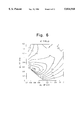
- FIG. 6 is a graph showing relationship of parameters kh z and kh s for the SAW device of "type D" at various effective coupling coefficients K 2 s, which was obtained in Example 4;
- FIG. 7 is a graph showing relationship of parameters kh z and kh s for the SAW device of "type E" at various effective coupling coefficients K 2 s, which was obtained in Example 5;
- FIG. 8 is a graph showing relationship of parameters kh z and kh s for the SAW device of "type F" at various effective coupling coefficients K 2 s, which was obtained in Example 6;
- FIG. 9 is a graph showing relationship of parameters kh z and kh s for the SAW device of "type G" at various effective coupling coefficients K 2 s, which was obtained in Example 7;
- FIG. 10 is a graph showing relationship of parameters kh z and kh s for the SAW device of "type A”, “type B”, “type C”, “type D”, “type E”, “type F” and “type G”, at various propagation velocities Vs;
- FIG. 11 is a graph showing relationship of parameters kh z and kh s for the SAW device of "type A”, “type B”, “type C”, “type D”, “type E”, “type F” and “type G”, at various TCFs;
- FIG. 12A schematically illustrates a planar shape of an IDT (single-type electrode).
- FIG. 12B schematically illustrates a planar shape of an IDT (double-type electrode).
- the diamond material preferable for the use in the present invention may be either natural diamond or synthetic diamond.
- the diamond may be single crystalline diamond or polycrystalline diamond.
- the diamond plate/substrate itself can be used for fabricating SAW devices according to the present invention.
- Diamond layer/film formed on the other base material can also be employed.
- the base material used for forming diamond film is not particularly limited, but may appropriately be selected depending on the usage of the SAW device.
- the base material to be available in the present invention may comprise semiconductor materials such as crystalline silicon, amorphus silicon, metals, glass and ceramics.
- the process may appropriately be selected from known synthesis processes such as CVD(Chemical Vapor Deposition) including microwave plasma CVD, plasma enhanced CVD, PVD(Physical Vapor Deposition), sputtering, ion plating, plasma jet method, flame method and hot filament method.
- the plane orientation of the diamond may be any of (111), (100) and (110), etc., or may be any combination of these plane orientations.
- ZnO layer that is disposed on the diamond and functions as piezoelectric layer of the SAW device according to the present invention, is preferably polycrystalline, and c-axis oriented, in view of piezoelectric property.
- c-axis oriented it is meant that ZnO layer have a (001) plane that is parallel to a base layer, such as diamond layer, on which the ZnO layer is disposed.
- SiO 2 layer that is formed on the ZnO layer and functions as protecting or passivating material for the ZnO layer and IDT according to the present invention, is preferably an amorphous SiO 2 layer, in view of formability and processability.
- SiO 2 layer can compensate the variation of the SAW propagation velocity through diamond and ZnO layers to provide the operation stability for temperature variation.
- a pair of IDTs are disposed at input side and output side.
- Any of electric conductive materials can be used for interdigital transducer for the SAW device of the present invention.
- Al aluminum
- Al may preferably be used as the material for the IDT.
- the thickness of the IDT is not limited, as long as it functions as an IDT of a SAW device.
- the thickness of the IDT may typically be in the range of about 100 to about 5,000 ⁇ (more preferably, about 100 to 500 ⁇ ).
- the electrode resistivity is increased, causing considerable energy loss.
- the thickness of the IDT exceeds 5,000 ⁇ , considerable mass addition effect cause reflection of SAW, and desired SAW characteristic of the SAW device may suffer.
- the planar or projected shape of the IDT for the SAW device of the present invention is not limited. Electrode called “single-type" electrode as shown in the schematic plan view of FIG. 12A or electrode called “double-type” electrode as shown in the schematic plan view of FIG. 12B may typically be used for the present invention.
- the short-circuiting electrode to be disposed as desired is an electrode having a function of providing an equipotential state to an electric field so as to change the SAW characteristics of the device.
- This electrode may preferably comprise a (thin) film of a metal such as Al, Au or Al-Cu. Since the short-circuiting electrode has different function from that of the IDT, the material of the short-circuiting electrode may not be same as that of the IDT.
- the thickness of the short-circuiting electrode is not particularly limited, as long as it can function as a short-circuiting electrode of a SAW device.
- the thickness of the short-circuiting electrode may preferably be in the range of about 50 to 3,000 ⁇ (more preferably, about 100 to 500 ⁇ ). When the thickness is less than 50 ⁇ , it is difficult to obtain an equipotential state as described above. On the other hand, when the thickness exceeds 3,000 ⁇ , it may affect the reflection of SAW.
- the short-circuiting electrode may preferably has a planner shape of a "solid electrode" having an area substantially equal to that of the IDT to be used in combination therewith.
- each of the SAW devices of Examples 1 includes: a 20 ⁇ m thick of diamond 20; one of ten different thicknesses within the range of 0.25 to 2.5 ⁇ m of ZnO layer; and one of ten different thicknesses within the range of 0.20 to 2.0 ⁇ m of SiO 2 .
- the desired thicknesses of ZnO and SiO 2 layers are expressed by the parameters kh z and kh s for 2nd mode SAW having wavelength ⁇ :
- a polycrystalline diamond film was formed on a (100) plane of monocrystalline silicon having dimension of 10 ⁇ 10 ⁇ 1 (mm) by microwave plasma CVD process.
- Diamond layer 12 having thickness of 20 ⁇ m was then deposited in the plasma created under the condition of:microwave power of 400 W, pressure of about 40 Torr and temperature of 850° C. The deposited diamond layer was allowed to stand for 10 minutes in the air of 450° C., to enhance the resistance of diamond layer.
- the Si substrate having diamond layer thereon was transferred to a vacuum chamber of a magnetron sputtering apparatus to deposit ZnO layer 14 onto the diamond layer 12.
- a polycrystalline ZnO target was included within the chamber.
- Aluminum IDTs 20 having planer shape of double-type electrode as shown in FIG. 12B were formed on ZnO layer 14 by resistance heating processing and subsequent etching.
- radio frequency (RF) power was applied to the input IDT to generate SAW of 2nd mode.
- the effective coupling coefficient (K 2 ) was also evaluated by measuring the radiation conductance (wherein the real part is denoted by "G") of the IDT by using a network analyzer ("Network Analyzer 8719A", commercially available from Yokogawa Hewlett Packard (YHP), Japan), and by using following formula:
- TCF measurement was carried out by the following manner: SAW device was heated by an external heater from room temperature to 70° C. The central frequency F 0 was measured at every 10° C. from the room temperature to 70° C. Proportional relationship between the central frequency and the device temperature. TCF was given by the slope of the relationship.
- propagation loss was evaluated by the following manner: SAW devices having same layer/electrode constitution but different spacing between input IDT and output IDT (e.g., 50 wavelength, 100 wavelength and 150 wave length) were fabricated. A relationship of insertion loss with the spacing was evaluated to be proportional. Then the propagation loss was obtained by the slop of the relationship.
- the thickness t z ( ⁇ m) of the ZnO layers of each SAW devices, and the thickness t s ( ⁇ m) of the SiO 2 layers of each SAW device were measured by cutting off the device after the measurement of device performances as described above, and observing the resultant section of the device with a scanning electron microscope (SEM) at a magnification of 1000-5000 ⁇ .
- SEM scanning electron microscope
- FIG. 3 is a graph having abscissa axis of kh z and ordinate axis of kh s , showing the relationship of the parameters kh z and kh s at the given effective coupling coefficient K 2 .
- the numerical value at each curve is the value of K 2 in %.
- measured propagation loss was 0.05 dB/wavelength for 1st mode SAW, and 0.03 dB/wavelength for 2nd mode SAW.
- Examples 2-7 following SAW devices were fabricated by similar fabricating processes as used in Example 1: "type B" SAW device 10b was made in Example 2; “type C” SAW device 10c was made in Example 3; “type D” SAW device 10d was made in Example 4; “type E” SAW device 10e was made in Example 5; “type F” SAW device 10f was made in Example 6; and “type G” SAW device log was made in Example 7.
- Example 2 type B
- Example 3 type C
- Example 4 type D
- IDT 20 was formed onto ZnO layer 14 after ZnO layer 14 had been deposited, as described in Example 1.
- Example 5 type E
- Example 6 type F
- Example 7 type G
- IDT 20 was formed by the same forming process as used in Example 1, after polishing the surface of diamond layer 12 and before depositing ZnO layer; and then ZnO layer 14 was deposited onto diamond layer 12 to cover IDT 20.
- short circuiting electrodes 22 and 24 are included in the SAW device.
- the formation of the short circuiting electrodes 22 and 24 was carried out by the following manner: in Examples 2 (B) and 6 (F), after diamond 12 was deposited and polished, an aluminum layer having thickness of 250 angstrom was formed by resistive heating method. Then the aluminum layer was patterned via conventional photolithography to form short circuiting electrode 22, which has a geometry corresponding to the location of IDT 20.
- short circuiting electrode 22 which has a geometry corresponding to the location of IDT 20
- SiO 2 layer 16 via similar process as used in Examples 2 and 6, after depositing SiO 2 layer 16.
- short circuiting electrode 22 was formed onto diamond 12
- short circuiting electrode 24 was formed onto ZnO layer 14.
- similar processing as used in Examples 2 and 3 was employed.
- Each of electrodes 22 and 24 has a geometry corresponding to the location of IDT 20.
- each of the SAW devices of each of the Examples 2-7 includes: a 20 ⁇ m thick of diamond 20; one of ten different thicknesses within the range of 0.25 to 2.5 ⁇ m of ZnO layer; and one of ten different thicknesses within the range of 0.20 to 2.0 ⁇ m of SiO 2 .
- the desired thicknesses of ZnO and SiO 2 layers are expressed by the parameters kh z and kh s for 2nd mode SAW having wavelength ⁇ , as in Example 1:
- Effective coupling coefficient K 2 of each of the SAW devices was evaluated by similar manner as used in Example 1.
- FIGS. 4 to 9 are graph having abscissa axis of kh z and ordinate axis of kh s , showing the relationship of the parameters kh z and kh s at the given effective coupling coefficient K 2 in Examples 2 to 7, respectively.
- the numerical value at each curve is the value of K 2 in %.
- FIG. 4 illustrates the relationship obtained in Example 2;
- FIG. 5 shows the results of Example 3;
- FIG. 6 shows the results of Example 4;
- FIG. 7 shows the results of Example 5;
- FIG. 8 shows the results of Example 6; and
- FIG. 9 shows the results of Example 7.
- the SAW device having improved performances can be fabricated to have ZnO and SiO 2 layers, that have the optimized dimensionless thickness kh z and kh s given in the region A-B-C-D-E-F-G-H-I-J-K-L-M-N-O-P-Q-R-A, outer edge of which is given by a closed chain consisting of points A, B, C, D, E, F, G, H, I, J, K, L, M, N, O, P, Q and R and lines A-B, B-C, C-D, D-E, E-F, F-G, G-H, H-I, I-J, J-K, K-L, L-M, M-N, N-O, O-P, P-Q, Q-R and R-A.
- This region is shown in FIG. 1.
- the SAW device is provided with further improved performances, when the SAW device have ZnO and SiO 2 layers, that have the optimized dimensionless thickness kh z and kh s given in the region A-B-C-D-S-T-M-N-O-P-Q-R-A, outer edge of which is given by a closed chain consisting of points A, B, C, D, S, T, M, N, O, P, Q and R and lines A-B, B-C, C-D, D-S, S-T, T-M, M-N, N-O, O-P, P-Q, Q-R and R-A. This region is also shown in FIG. 1.
- Points B to T in the coordinate graph (kh z , kh s ) also represent the following points:
- the SAW device is also provided with propagation loss of 0.05 (dB/ ⁇ ) for 1st mode SAW, and 0.03 (dB/ ⁇ ) for 2nd mode SAW. Further, such constitution has an advantage in fabricating process.
- the SAW device is also provided with propagation loss of 0.05 (dB/ ⁇ ) for 1st mode SAW, and 0.03 (dB/ ⁇ ) for 2nd mode SAW. Further, such constitution has an advantage in fabricating process.
- the SAW device is also provided with propagation loss of 0.05 (dB/ ⁇ ) for 1st mode SAW, and 0.03 (dB/ ⁇ ) for 2nd mode SAW. Further, such constitution has an advantage in fabricating process.
- the SAW device is also provided with propagation loss of 0.05 (dB/ ⁇ ) for 1st mode SAW, and 0.03 (dB/ ⁇ ) for 2nd mode SAW. Further, such constitution has an advantage in fabricating process.
- the SAW device is also provided with propagation loss of 0.05 (dB/ ⁇ ) for 1st mode SAW, and 0.03 (dB/ ⁇ ) for 2nd mode SAW. Further, such constitution has an advantage in fabricating process.
- the SAW device is also provided with propagation loss of 0.05 (dB/ ⁇ ) for 1st mode SAW, and 0.03 (dB/ ⁇ ) for 2nd mode SAW. Further, such constitution has an advantage in fabricating process.
- the SAW device is also provided with propagation loss of 0.05 (dB/ ⁇ ) for 1st mode SAW, and 0.03 (dB/ ⁇ ) for 2nd mode SAW. Further, such constitution has an advantage in fabricating process.
- the SAW device is also provided with propagation loss of 0.05 (dB/ ⁇ ) for 1st mode SAW, and 0.03 (dB/ ⁇ ) for 2nd mode SAW. Further, such constitution has an advantage in fabricating process.
- the SAW device is also provided with propagation loss of 0.05 (dB/ ⁇ ) for 1st mode SAW, and 0.03 (dB/ ⁇ ) for 2nd mode SAW. Further, such constitution has an advantage in fabricating process.
Landscapes
- Physics & Mathematics (AREA)
- Acoustics & Sound (AREA)
- Surface Acoustic Wave Elements And Circuit Networks Thereof (AREA)
Priority Applications (2)
| Application Number | Priority Date | Filing Date | Title |
|---|---|---|---|
| US08/791,894 US5783896A (en) | 1995-08-08 | 1997-01-31 | Diamond-Zn0 surface acoustic wave device |
| US08/964,469 US5959389A (en) | 1995-08-08 | 1997-11-04 | Diamond-ZnO surface acoustic wave device |
Applications Claiming Priority (2)
| Application Number | Priority Date | Filing Date | Title |
|---|---|---|---|
| JP7-202114 | 1995-08-08 | ||
| JP20211495A JP3205978B2 (ja) | 1995-08-08 | 1995-08-08 | 表面弾性波素子 |
Related Child Applications (1)
| Application Number | Title | Priority Date | Filing Date |
|---|---|---|---|
| US08/791,894 Continuation-In-Part US5783896A (en) | 1995-08-08 | 1997-01-31 | Diamond-Zn0 surface acoustic wave device |
Publications (1)
| Publication Number | Publication Date |
|---|---|
| US5814918A true US5814918A (en) | 1998-09-29 |
Family
ID=16452198
Family Applications (1)
| Application Number | Title | Priority Date | Filing Date |
|---|---|---|---|
| US08/689,296 Expired - Lifetime US5814918A (en) | 1995-08-08 | 1996-08-07 | Diamond-ZnO surface acoustic wave device |
Country Status (4)
| Country | Link |
|---|---|
| US (1) | US5814918A (fr) |
| EP (1) | EP0758165A1 (fr) |
| JP (1) | JP3205978B2 (fr) |
| CA (1) | CA2182829A1 (fr) |
Cited By (7)
| Publication number | Priority date | Publication date | Assignee | Title |
|---|---|---|---|---|
| US5959389A (en) * | 1995-08-08 | 1999-09-28 | Sumitomo Electronic Industries, Ltd. | Diamond-ZnO surface acoustic wave device |
| US6469416B1 (en) * | 2000-03-24 | 2002-10-22 | Sumitomo Electric Industries, Ltd. | Surface acoustic wave device |
| US6642813B1 (en) * | 1999-10-15 | 2003-11-04 | Sumitomo Electric Industries, Ltd. | Surface acoustic wave device utilizing a ZnO layer and a diamond layer |
| US20040183397A1 (en) * | 2000-05-31 | 2004-09-23 | Kam Chan Hin | Surface acoustic wave device |
| US20070296306A1 (en) * | 2004-09-17 | 2007-12-27 | Markus Hauser | Saw-Component Having a Reduced Temperature Path and Method for the Production Thereof |
| US20100038993A1 (en) * | 2008-08-13 | 2010-02-18 | Seiko Epson Corporation | Surface acoustic wave element |
| US20230077545A1 (en) * | 2020-01-23 | 2023-03-16 | Luxembourg Institute Of Science And Technology (List) | Passivated transparent piezoelectric device with high transparency and high breakdown voltage |
Families Citing this family (6)
| Publication number | Priority date | Publication date | Assignee | Title |
|---|---|---|---|---|
| JP3205978B2 (ja) * | 1995-08-08 | 2001-09-04 | 住友電気工業株式会社 | 表面弾性波素子 |
| MY129974A (en) * | 1996-11-07 | 2007-05-31 | Sumitomo Electric Industries | Diamond-zn0 surface acoustic wave device |
| EP1225693B1 (fr) | 1999-10-15 | 2008-05-21 | Seiko Epson Corporation | Dispositif saw |
| CA2401050A1 (fr) | 2000-03-24 | 2001-09-27 | Seiko Epson Corporation | Element a onde acoustique de surface |
| CN101584115B (zh) * | 2006-12-27 | 2012-09-05 | 株式会社村田制作所 | 声表面波装置 |
| WO2008111325A1 (fr) * | 2007-03-12 | 2008-09-18 | Murata Manufacturing Co., Ltd. | Dispositif à onde acoustique de surface |
Citations (7)
| Publication number | Priority date | Publication date | Assignee | Title |
|---|---|---|---|---|
| JPH03198412A (ja) * | 1989-12-26 | 1991-08-29 | Sumitomo Electric Ind Ltd | 表面弾性波素子 |
| EP0588261A1 (fr) * | 1992-09-14 | 1994-03-23 | Sumitomo Electric Industries, Limited | Elément à ondes acoustiques de surface |
| EP0608864A2 (fr) * | 1993-01-29 | 1994-08-03 | Sumitomo Electric Industries, Limited | Dispositif à ondes acoustiques de surface et sa méthode de fabrication |
| JPH0832398A (ja) * | 1994-05-10 | 1996-02-02 | Sumitomo Electric Ind Ltd | 表面弾性波素子 |
| JPH0865088A (ja) * | 1994-06-16 | 1996-03-08 | Sumitomo Electric Ind Ltd | 表面弾性波素子 |
| EP0758165A1 (fr) * | 1995-08-08 | 1997-02-12 | Sumitomo Electric Industries, Ltd. | Dispositif à ondes acoustiques de surface à diamant-ZnO |
| EP0766383A2 (fr) * | 1995-09-29 | 1997-04-02 | Sumitomo Electric Industries, Ltd. | Dispositif à ondes acoustiques de surface à diamant-ZnO comportant une couche relativement mince de ZnO piézoélectrique |
-
1995
- 1995-08-08 JP JP20211495A patent/JP3205978B2/ja not_active Expired - Lifetime
-
1996
- 1996-08-07 US US08/689,296 patent/US5814918A/en not_active Expired - Lifetime
- 1996-08-07 CA CA002182829A patent/CA2182829A1/fr not_active Abandoned
- 1996-08-07 EP EP96112749A patent/EP0758165A1/fr not_active Ceased
Patent Citations (11)
| Publication number | Priority date | Publication date | Assignee | Title |
|---|---|---|---|---|
| JPH03198412A (ja) * | 1989-12-26 | 1991-08-29 | Sumitomo Electric Ind Ltd | 表面弾性波素子 |
| EP0588261A1 (fr) * | 1992-09-14 | 1994-03-23 | Sumitomo Electric Industries, Limited | Elément à ondes acoustiques de surface |
| US5446329A (en) * | 1992-09-14 | 1995-08-29 | Sumitomo Electric Industries, Ltd. | Surface acoustic wave element |
| EP0608864A2 (fr) * | 1993-01-29 | 1994-08-03 | Sumitomo Electric Industries, Limited | Dispositif à ondes acoustiques de surface et sa méthode de fabrication |
| US5426340A (en) * | 1993-01-29 | 1995-06-20 | Sumitomo Electric Industries, Ltd. | Surface acoustic wave device and method of manufacturing the same |
| JPH0832398A (ja) * | 1994-05-10 | 1996-02-02 | Sumitomo Electric Ind Ltd | 表面弾性波素子 |
| US5565725A (en) * | 1994-05-10 | 1996-10-15 | Sumitomo Electric Industries, Ltd. | Surface acoustic wave device |
| JPH0865088A (ja) * | 1994-06-16 | 1996-03-08 | Sumitomo Electric Ind Ltd | 表面弾性波素子 |
| US5646468A (en) * | 1994-06-16 | 1997-07-08 | Sumitomo Electric Industries, Ltd. | Diamond-LiTaO3 surface acoustic wave device |
| EP0758165A1 (fr) * | 1995-08-08 | 1997-02-12 | Sumitomo Electric Industries, Ltd. | Dispositif à ondes acoustiques de surface à diamant-ZnO |
| EP0766383A2 (fr) * | 1995-09-29 | 1997-04-02 | Sumitomo Electric Industries, Ltd. | Dispositif à ondes acoustiques de surface à diamant-ZnO comportant une couche relativement mince de ZnO piézoélectrique |
Non-Patent Citations (2)
| Title |
|---|
| Mitsuyu et al., "Structures and SAW Properties of rf-sputtered single-crystalline films of ZnO on sapphire", J. Appl.Phys. 51(5): 2464-2470 (May 1980). |
| Mitsuyu et al., Structures and SAW Properties of rf sputtered single crystalline films of ZnO on sapphire , J. Appl.Phys. 51(5): 2464 2470 (May 1980). * |
Cited By (10)
| Publication number | Priority date | Publication date | Assignee | Title |
|---|---|---|---|---|
| US5959389A (en) * | 1995-08-08 | 1999-09-28 | Sumitomo Electronic Industries, Ltd. | Diamond-ZnO surface acoustic wave device |
| US6642813B1 (en) * | 1999-10-15 | 2003-11-04 | Sumitomo Electric Industries, Ltd. | Surface acoustic wave device utilizing a ZnO layer and a diamond layer |
| US6469416B1 (en) * | 2000-03-24 | 2002-10-22 | Sumitomo Electric Industries, Ltd. | Surface acoustic wave device |
| US20040183397A1 (en) * | 2000-05-31 | 2004-09-23 | Kam Chan Hin | Surface acoustic wave device |
| US20070296306A1 (en) * | 2004-09-17 | 2007-12-27 | Markus Hauser | Saw-Component Having a Reduced Temperature Path and Method for the Production Thereof |
| US7589452B2 (en) * | 2004-09-17 | 2009-09-15 | Epcos Ag | SAW-component having a reduced temperature path and method for the production thereof |
| US20100038993A1 (en) * | 2008-08-13 | 2010-02-18 | Seiko Epson Corporation | Surface acoustic wave element |
| US8004148B2 (en) | 2008-08-13 | 2011-08-23 | Seiko Epson Corporation | Surface acoustic wave element |
| US20230077545A1 (en) * | 2020-01-23 | 2023-03-16 | Luxembourg Institute Of Science And Technology (List) | Passivated transparent piezoelectric device with high transparency and high breakdown voltage |
| US12382835B2 (en) * | 2020-01-23 | 2025-08-05 | Luxembourg Institute Of Science & Technology (List) | Passivated transparent piezoelectric device with high transparency and high breakdown voltage |
Also Published As
| Publication number | Publication date |
|---|---|
| JP3205978B2 (ja) | 2001-09-04 |
| CA2182829A1 (fr) | 1997-02-09 |
| JPH0951248A (ja) | 1997-02-18 |
| EP0758165A1 (fr) | 1997-02-12 |
Similar Documents
| Publication | Publication Date | Title |
|---|---|---|
| EP0588261B1 (fr) | Elément à ondes acoustiques de surface | |
| EP0608864B1 (fr) | Dispositif à ondes acoustiques de surface et sa méthode de fabrication | |
| US5646468A (en) | Diamond-LiTaO3 surface acoustic wave device | |
| US5777422A (en) | Diamond-ZnO surface acoustic wave device having relatively thinner ZnO piezoelectric layer | |
| US5838090A (en) | Surface acoustic wave device | |
| Wu et al. | Growth of ZnO thin films on interdigital transducer/Corning 7059 glass substrates by two-step fabrication methods for surface acoustic wave applications | |
| EP0758165A1 (fr) | Dispositif à ondes acoustiques de surface à diamant-ZnO | |
| JP3318920B2 (ja) | 表面弾性波素子 | |
| US5783896A (en) | Diamond-Zn0 surface acoustic wave device | |
| US5959389A (en) | Diamond-ZnO surface acoustic wave device | |
| US20020158549A1 (en) | Surface acoustic wave device | |
| US6713941B2 (en) | Surface acoustic wave element | |
| EP0841749B1 (fr) | Dispositif à ondes acoustiques de surface à diamant-ZnO | |
| JP3365505B2 (ja) | 表面弾性波素子 | |
| JP3753076B2 (ja) | 3次モードの5倍高調波を利用する表面弾性波素子 | |
| JP3365506B2 (ja) | 表面弾性波素子 | |
| Fujii et al. | A diamond substrate suitable for 5GHz SAW device application | |
| JPS59210716A (ja) | 表面波デバイス用基板 |
Legal Events
| Date | Code | Title | Description |
|---|---|---|---|
| AS | Assignment |
Owner name: SUMITOMO ELECTRIC INDUSTRIES, LTD., JAPAN Free format text: ASSIGNMENT OF ASSIGNORS INTEREST;ASSIGNORS:NAKAHATA, HIDEAKI;HIGAKI, KENJIRO;FUJII, SATOSHI;AND OTHERS;REEL/FRAME:008180/0143 Effective date: 19960906 |
|
| STCF | Information on status: patent grant |
Free format text: PATENTED CASE |
|
| FEPP | Fee payment procedure |
Free format text: PAYOR NUMBER ASSIGNED (ORIGINAL EVENT CODE: ASPN); ENTITY STATUS OF PATENT OWNER: LARGE ENTITY |
|
| FPAY | Fee payment |
Year of fee payment: 4 |
|
| AS | Assignment |
Owner name: SEIKO EPSON CORPORATION, JAPAN Free format text: ASSIGNMENT OF ASSIGNORS INTEREST;ASSIGNOR:SUMITOMO ELECTRIC INDUSTRIES, LTD.;REEL/FRAME:014567/0509 Effective date: 20040312 |
|
| FPAY | Fee payment |
Year of fee payment: 8 |
|
| FPAY | Fee payment |
Year of fee payment: 12 |