EP0608864A2 - Dispositif à ondes acoustiques de surface et sa méthode de fabrication - Google Patents
Dispositif à ondes acoustiques de surface et sa méthode de fabrication Download PDFInfo
- Publication number
- EP0608864A2 EP0608864A2 EP94101135A EP94101135A EP0608864A2 EP 0608864 A2 EP0608864 A2 EP 0608864A2 EP 94101135 A EP94101135 A EP 94101135A EP 94101135 A EP94101135 A EP 94101135A EP 0608864 A2 EP0608864 A2 EP 0608864A2
- Authority
- EP
- European Patent Office
- Prior art keywords
- acoustic wave
- surface acoustic
- wave device
- diamond
- layer
- Prior art date
- Legal status (The legal status is an assumption and is not a legal conclusion. Google has not performed a legal analysis and makes no representation as to the accuracy of the status listed.)
- Granted
Links
Images


Classifications
-
- H—ELECTRICITY
- H03—ELECTRONIC CIRCUITRY
- H03H—IMPEDANCE NETWORKS, e.g. RESONANT CIRCUITS; RESONATORS
- H03H9/00—Networks comprising electromechanical or electro-acoustic elements; Electromechanical resonators
- H03H9/02—Details
- H03H9/02535—Details of surface acoustic wave devices
- H03H9/02543—Characteristics of substrate, e.g. cutting angles
- H03H9/02582—Characteristics of substrate, e.g. cutting angles of diamond substrates
Definitions
- the present invention relates to a surface acoustic wave device which operates in a high-frequency range including several hundreds of MHz to GHz and more particularly to the surface acoustic wave device which comprises diamond or a diamond-like carbon film and a piezoelectric body and a method for manufacturing the same.
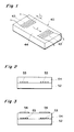
- a surface acoustic wave device is an electro-mechanical conversion device utilizing a surface wave propagating on the surface of an elastic body and has a basic structure shown in Fig. 1.
- a surface acoustic wave device 40 the piezoelectric phenomenon of a piezoelectric body 44 is used in exciting a surface acoustic wave.
- an electrical signal is applied to one interdigital transducer (comb-like electrode) 43 formed on the piezoelectric body 44, the piezoelectric body 44 is stressed, and this stress becomes a surface acoustic wave. Then, the surface acoustic wave propagates on the piezoelectric body 44 and is extracted as an electrical signal at the other interdigital transducer 43'.
- the surface acoustic wave device requires a small number of parts and can be miniaturized. In addition, signals can be easily taken in and out on a surface acoustic wave propagation path.
- This device can be used in a variety of applications such as a filter, a delay line, an oscillator, a resonator, a convolver, or a correlator.
- the surface acoustic wave device has been used as an IF television filter.
- Such surface acoustic wave devices have also been tested as filters for VTRs and various communication apparatus such as a car telephone, a cellular phone and so on.
- a typical conventional surface acoustic device is a device having a structure in which interdigital transducers are formed on a crystalline piezoelectric body such as LiNb0 3 or LiTa0 3 .
- Another surface acoustic wave device having a piezoelectric thin film of ZnO or others sputtered on a base substrate of glass or others is used.
- a device in which interdigital transducers are formed on a single crystalline piezoelectric body without any other consideration cannot have a high center frequency in excess of 1 GHz because its surface acoustic wave propagation velocity V is low.
- a space Xo between each of the electrodes has to be smaller or the surface acoustic wave propagation velocity V has to be increased.
- a device in which a sapphire layer having a larger propagation velocity of the surface acoustic wave than that of the piezoelectric body is placed between a base substrate and a piezoelectric layer is disclosed in Japanese Patent Laid-Open No. 54-38874(38874/1979). Further, a device in which a piezoelectric layer is deposited on a diamond layer in order to increase a propagation velocity of the surface acoustic wave is disclosed in Japanese Patent Laid-Open No. 64-62911(62911/1989) by Imai and others and Japanese Patent Laid-Open No. 3-198412(198412/1991) by Nakahata and others. Fig. 2-Fig. 5 show the devices disclosed in these reference.
- a piezoelectric layer 54 is formed on a diamond layer 52 and between these layer, interdigital transducers 53 are formed.
- short circuiting electrodes 56 are placed on the piezoelectric layer 54 of the device shown in Fig. 2.
- a piezoelectric layer 54 is formed on a diamond layer 52, and interdigital transducers 53 are placed on the piezoelectric layer 54.
- the device shown in Fig. 5 comprises the short circuiting electrodes 56 placed between the piezoelectric layer 54 and the diamond layer 52 of the device shown in Fig. 4.
- a surface acoustic wave device of the present invention comprises a hard layer comprising diamond as a composition component, a piezoelectric layer formed on the hard layer, a group of a pair of electrodes, placed in apart, for performing electro-mechanical conversion, and a grounding electrode comprising a conductive oxide, placed corresponding to each of the electrodes.
- the group of a pair of electrodes and the grounding electrode is formed with the piezoelectric layer between, and either the group of a pair of electrodes or the grounding electrode is formed on the hard layer.
- the grounding electrode is formed of a conductive oxide, so that crystalline turbulence in interface between the grounding electrode and the hard layer or between the grounding electrode and the piezoelectric layer can be remarkably suppressed and the adhesive can be enhanced.
- the hard layer comprises diamond or a diamond-like carbon film.
- a layer comprising dioxide silicon is formed on the piezoelectric layer.
- a conductive oxide forming the grounding electrode is formed by doping an impurity into material constituting piezoelectric body.
- a method for manufacturing a surface acoustic wave device of the present invention comprises a step of forming a hard layer comprising diamond as a composition component on a base substrate, a step of forming a piezoelectric layer comprising a piezoelectric material, a step of forming a group of a pair of electrodes, placed in apart, for performing electro-mechanical conversion, and a step of forming a grounding electrode comprising the conductive oxide.
- it preferably comprises a step of forming a layer comprising dioxide silicon on both the piezoelectric layer and a pair of electrodes.
- a surface acoustic wave device according to the present invention will be explained more particularly prior to explaining the embodiments.
- a diamond-like carbon film which is a hard layer comprising diamond is called i-carbon.
- the diamond-like carbon film is found in the process of studies on deposition syntheses of diamond. The physical properties of the i-carbon have been examined and clarified by many of researchers. Although there is no theory which defines the diamond-like carbon film as one material, this film is apparently different from diamond or graphite and preferably has the following properties.
- the diamond-like carbon film which has such a noncrystalline structure, crystalline diamond and graphite can be distinguished by Raman spectroscopic analysis disclosed in a reference below. Typical Raman spectrum is shown in Fig. 8, p. 47 of the reference. The sharp spectrum is seen at 1332 cm- 1 for diamond and at 1580 cm- 1 for graphite whereas the wide spectrum is seen at 1360 cm- 1 and 1600 cm- 1 for the diamond-like carbon film (noncrystalline structure).
- diamond has hardness of up to 10,000(Hv), while the diamond-like carbon film has hardness of 1,000 to 5,000 (Hv). It is noted that the hardness described herein is obtained by a Vickers Hardness test.
- resistivity of diamond and the diamond-like carbon film is suitable but approximately 10 6 Qcm-108 Qcm is preferred. It is noted that the resistivity described herein is obtained by a four probe method.
- the diamond-like carbon film is manufactured by an deposition (e.g., vapor phase deposition) process such as plasma CVD, ion beam deposition, or sputtering, which is basically the same as the manufacturing process of the diamond thin layer described hereinafter.
- vapor phase deposition e.g., plasma CVD, ion beam deposition, or sputtering
- the hard layer may comprise a small amount of impurity.
- the hard layer comprising high purity diamond is preferably used from the viewpoint of a higher surface acoustic wave propagation velocity and a higher electro-mechanical conversion efficiency. That is, it is preferred that the hard layer comprises diamond as a composition component.
- the diamond-like carbon film is deposited synthesized even at room temperature while diamond requires a synthesis temperature of 500 ° C or higher. For this reason, the diamond-like carbon film makes it possible to widen the selection of a base substrate on which the diamond-like carbon film is to be formed.
- the diamond-like carbon film having a large area can be easily formed and has a flatter surface compared to diamond.
- the hard layer may consist of natural single crystalline diamond or single crystalline diamond synthesized at a very high pressure.
- the hard layer may be a layer of the diamond thin film formed on a base substrate or a diamond-like carbon film.
- the thickness of the hard layer is preferably in excess of 0.4 times the wavelength of propagating surface acoustic waves and more preferably in excess of 0.6 times.
- the base substrate on which the diamond thin film is to be formed is not limited to a specific one, but preferably comprises of semiconductor material or an inorganic material such as Si, Mo, Cu, Ni, W, GaAs, or LiXb0 3 .
- the base substrate on which the diamond-like carbon film to be formed makes it possible to select a base substrate in a wider range than that for diamond.
- a base substrate includes a base substrate comprising an organic compound such as a synthetic resin.
- the diamond thin film formed on the base substrate may be single crystalline or polycrystalline diamond.
- the diamond thin film formed by vapor phase deposition synthesis generally has a polycrystalline structure.
- a method of forming a diamond thin film on a base substrate is a CVD method such as a thermal CVD method, a plasma CVD method, a microwave CVD method, a photo-CVD method, or a laser CVD method, sputtering or ion beam deposition.
- the diamond-like carbon film may be formed on a base substrate by the same forming method as the diamond thin film.
- a method of decomposing and exciting a source gas to grow a diamond thin film is enumerated as follows:
- a source material used to synthesize a diamond thin film or a diamond-like carbon film is generally a carbon-containing compound and preferably used in combination with hydrogen gas.
- An oxygen-containing compound and/or an inert gas may be added to the source gas, as needed.
- the preferred examples of the carbon-containing compound are a paraffin-based hydrocarbon (e.g., methane, ethane, propane, or butane), an olefin-based hydrocarbon (e.g., ethylene, propylene, or butylene), an acetylene-based hydrocarbon (e.g., acetylene or allylene), a diolefin-based hydrocarbon (e.g., butadiene), an alicyclic hydrocarbon (e.g., cyclopropane, cyclobutane, cyclopentane, or cyclohexane), an aromatic hydrocarbon (e.g., cyclobutadiene, benzene, toluene, or cyclohexane), ketones (e.g., acetone, diethyl ketone, and benzophenone), alcohols (e.g., methanol and ethanol), amines (trimethylamine and triethylamine), carbon
- oxygen-containing compound added to the source gas water, carbon monoxide, carbon dioxide, or hydrogen peroxide is preferable because it is easily accessible.
- the preferred examples of the inert gas which can be added to the source gas are argon, helium, neon, krypton, xenon, and radon.
- the hard layer may be constituted by a base substrate consisting essentially of single crystalline diamond.
- the single crystalline diamond base substrate is preferably used to increase the surface acoustic wave propagation velocity and the electro-mechanical coupling coefficient. It is preferred that such a base substrate comprises natural diamond or synthetic diamond synthesized at a very high pressure.
- the piezoelectric layer comprises a piezoelectric material such as ZnO, AIN, Pb(Zr,Ti)0 3 , (Pb,La)(Zr,Ti)0 3 , LiTa0 3 , LiNb0 3 , Si0 2 , Ta 2 0 5 , Nb 2 0 5 , BeO, Li2B4.07, KNb0 3 , ZnS, ZnSe, or CdS.
- a piezoelectric material such as ZnO, AIN, Pb(Zr,Ti)0 3 , (Pb,La)(Zr,Ti)0 3 , LiTa0 3 , LiNb0 3 , Si0 2 , Ta 2 0 5 , Nb 2 0 5 , BeO, Li2B4.07, KNb0 3 , ZnS, ZnSe, or CdS.
- the piezoelectric layer may comprise either a single crystalline or polycrystalline piezoelectric material but in order to use a device in a higher-frequency range, the piezoelectric layer preferably comprises a single crystalline material in which a surface acoustic wave is scattered less compared to the polycrystalline material.
- a layer comprising a piezoelectric material such as ZnO, AIN, or PB(Zr,Ti)0 3 is preferably formed by a CVD method or sputtering.
- a group of a pair of electrodes which perform the electro-mechanical conversion is typically a comb-like electrode or an electrode group called interdigital transducer (IDT).
- IDT interdigital transducer
- the interdigital transducer having the configuration as shown in Fig. 6 and Fig. 7 is used.
- the interdigital transducer can be manufactured to have an electrode spacing of about 1.2 /1 .m using the photolithographic technique.
- a material for forming the electrode is preferably a metal having a low resistivity and for example, a metal such as Au, Ag, and AI which can be deposited at a low temperature, and a refractory metal such as Ti, W, and Mo are preferably used.
- AI and Ti are preferably used to facilitate formation of electrodes.
- W and Mo are preferably used to improve adhesion properties with diamond.
- the interdigital transducer may be formed of a single metal material or a combination of two or more metal materials such that AI is deposited on Ti.
- a metal layer selectively comprising the above materials is formed at a predetermined location.
- a resist film is formed on the metal layer and thereafter a mask having a interdigital transducer pattern formed on a transparent flat plate of glass is placed above the resist film, and the resist film is exposed with a mercury lamp. Thereafter, the exposed resist film is developed to obtain a resist pattern.
- the resist pattern may be formed by a method of directly exposing a resist film with an electron beam other than the above- mentioned method.
- the metal layer is patterned into a predetermined shape by etching.
- etching a layer comprising a metal having a low melting point such as Al
- an alkaline solution such as a sodium hydroxide solution or an acidic solution such as a nitric acid solution is used.
- a solution mixture of hydrofluoric acid and nitric acid is used. Reactive ion etching using a gas such as BC1 3 may be used to etch the metal layer.
- a group of a pair of the electrodes may also be formed of diamond (semiconductor diamond) having electrical conductivity.
- the conductive diamond is formed by a method of epitaxially growing diamond while doping an impurity such as P, Al, P, or S, a method of doping such an impurity to insulating diamond by ion implantation, a method of radiating insulating diamond with an electron beam to introduce lattice defects, or a method of hydrogenating insulating diamond.
- a surface acoustic wave device according to the present invention is shown in Fig. 8 - Fig. 13.
- a surface acoustic wave device shown in Fig. 8 comprises a diamond thin film 2 as a hard layer formed on an Si base substrate 1, and a pair of grounding electrodes 3 placed in apart on the diamond thin film 2.
- the grounding electrodes 3 are formed of an electrically conductive oxide.
- a piezoelectric layer 4 is formed so that it covers the grounding electrodes 3 and the diamond thin film 2.
- interdigital transducers 5 as a group of a pair of electrodes is formed in a position corresponding to each grounding electrode 3 on the piezoelectric layer 4.
- the grounding electrodes 3 and the interdigital transducers 5 can be exchanged.
- an Si0 2 film 6 may be formed on a top surface of the device shown in Fig. 8 and Fig. 9.
- grounding electrodes 3 may be formed on the Si0 2 film 6 of the device shown in Fig. 10 and Fig. 11. It is noted that inventors of the present invention applied for the invention relating to placing the Si0 2 film to the surface acoustic wave device (U.S. Patent Application No. 08/118,976).
- the grounding electrodes 3 of an electrically conductive oxide are sandwiched either between the diamond thin film 2 as a hard layer and the piezoelectric layer 4 or between the piezoelectric layer 4 and the Si0 2 film 6, so that electromechanical coupling is enhanced.
- the piezoelectric layer and the grounding electrodes may be formed of different material, and they may be formed of basically the same material.
- the piezoelectric layer and the grounding electrodes are formed of the same material, adhesive in interface between the piezoelectric layer and the grounding electrodes in the surface acoustic wave device can be enhanced more compared to a case that they are formed of different materials.
- the piezoelectric layer and the grounding electrodes are formed of the same material, for example it is preferred that the piezoelectric layer is formed of some piezoelectric material and the grounding electrodes are formed of material(oxide) having electrical conductivity by doping an impurity to the piezoelectric material. More particularly, the piezoelectric layer is formed of ZnO and the grounding electrodes are formed of ZnO having electrical conductivity by doping a metal element such as Al, V, Ga or In to this ZnO. Both ZnO having electrical conductivity and ZnO as a piezoelectric body have almost the same crystal structure and composition, and their adhesion is the highest.
- the grounding electrodes can be formed of a conductive oxide including metal oxide, such as Sn0 2 , ln 2 0 3 , TiO, LiV 2 0 4 , Re0 3 , LaTi0 3 , SrV0 3 , CaCr0 3 , V 2 0 3 , V0 2 , Cr0 2 or Ir0 2 , which is non piezoelectric material.
- metal oxide such as Sn0 2 , ln 2 0 3 , TiO, LiV 2 0 4 , Re0 3 , LaTi0 3 , SrV0 3 , CaCr0 3 , V 2 0 3 , V0 2 , Cr0 2 or Ir0 2 , which is non piezoelectric material.
- the piezoelectric layer is formed of some piezoelectric material and the grounding electrodes can be formed of piezoelectric material to which conductivity is added by doping an impurity other than the piezoelectric material used in the piezoelectric layer. More particularly, the piezoelectric layer can be formed of piezoelectric material such as AIN, PB(Zr, Ti)03, LiTa0 3 or Si0 2 , and the grounding electrodes can be formed of ZnO to which a metal element such as Al, V, Ga or In is doped.
- the grounding electrodes are formed of piezoelectric material such as ZnO having electrical conductivity
- sputtering using a target of sintered body including metal oxide such as A1 2 0 3 , V 2 0 3 , Ga 2 0 3 or ln 2 0 3 is preferably used.
- the grounding electrode is formed of the electrically conductive oxide which is not a piezoelectric material, sputtering, an ion-plating method or an electron beam (EB) deposition method is preferably used.
- Resistivity of the grounding electrode is preferably less than 10 -2 ⁇ cm and more preferably less than 10 -3 ⁇ cm in order to function sufficiently as a grounding electrode.
- Resistivity of the piezoelectric layer is preferably more than 105 Qcm. It is noted that each resistivity is measured based on the four probe method.
- a layer comprising dioxide silicon (Si0 2 ) is preferably deposited by a sputtering method, an ion-plating method, a CVD method, an electron beam (EB) deposition method or a low temperature CVD method.
- Dioxide silicon (Si0 2 ) may be either crystal or noncrystal.
- each layer and each electrode is shown. Thickness of a hard layer is greater or equal to 1 ⁇ m, thickness of a piezoelectric layer is 1000 angstroms to 5 ⁇ m, thickness of a group of electrodes is 100 angstroms to 1000 angstroms, thickness of a grounding electrode is 100 angstroms to 1 ⁇ m, and thickness of a layer comprising dioxide is 1000 angstroms to 5 ⁇ m.
- the adhesive between the grounding electrodes and the hard layer or between the grounding electrodes and the piezoelectric layer is high enough even though the stress is added to the grounding electrodes, so that detachment is hardly occurred, not like the conventional one. Therefore, excellent characteristics of the device can be achieved without any surface acoustic wave scattering or deterioration.
- the device has the resistant structure against a variation of temperature during the manufacturing process, so that yielding of the device can be improved.
- the surface acoustic wave device which can increase the yielding of device and has high electromechanical conversion efficiency in a high frequency range can be provided.
- An Si base substrate having dimensions of 10 X 10 X 1 mm was prepared and placed in a plasma CVD apparatus.
- Plasma CVD was performed under the condition that is a vacuum chamber pressure of about 40 Torr, a base substrate temperature of 850 ° C, and a microwave power of 400 W to grow a 30 ⁇ m thick diamond thin film (hard layer) on the Si base substrate.
- the diamond thin film was left in atmosphere of the reaction chamber at 450 ° C for 10 minutes to increase the resistivity of the diamond thin film.
- a surface of the diamond thin film was machine polished using an electro-deposited diamond grindstone, and thereafter magnetron-sputtered using a target of ZnO polycrystalline body including alumina (A1 2 0 3 ).
- a target of ZnO polycrystalline body including alumina A1 2 0 3 .
- the insulating ZnO thin film to which 2.0 atomic % Li to ZnO was doped was deposited to 5.0 ⁇ m thickness.
- interdigital transducers (a group of electrodes) having a 2 ⁇ m space between each of the electrodes were formed on the AI layer by using a photolithography method.
- the interdigital transducer shape is similar to the one shown in Fig. 6.
- Fig. 8 is a sectional view showing a surface acoustic wave device based on the first embodiment with such a structure as described above.
- a diamond thin film 2 is formed on an Si base substrate 1 and grounding electrodes 3 comprising conductive ZnO are formed on the diamond thin film 2, and a piezoelectric layer 4 comprising insulating ZnO thereon. Further, interdigital transducers 5 are formed on the piezoelectric layer 4.
- a surface acoustic wave device was manufactured following the same procedures as in the surface acoustic wave device based on the first embodiment, except that the 500 angstroms grounding electrodes comprising metal AI were formed by a vacuum vapor deposition method.
- a diamond thin film is formed on an Si base substrate, and a grounding electrodes comprising AI are formed on the diamond thin film, and further a piezoelectric layer comprising insulating ZnO is formed thereon. Moreover, interdigital transducers are formed on the piezoelectric layer.
- an Si base substrate having dimensions of 10 X 10 X 1 mm was prepared and placed in a plasma CVD apparatus.
- Plasma CVD was performed under the condition that was a vacuum chamber pressure of about 40 Torr, a base substrate temperature of 850 ° C, and a microwave power of 400 W to grow a 30 ⁇ m thick diamond thin film (hard layer) on the Si substrate.
- the diamond thin film was left in the atmosphere of the reaction chamber at 450 °C for 10 minutes to increase the resistivity of the diamond thin film.
- a surface of the diamond thin film was machine polished, and thereafter magnetron-sputtered using a target of ZnO polycrystalline body including Ga 2 0 3 (A1 2 0 3 ).
- the insulating ZnO thin film to which 2.0 atomic % Li to ZnO was doped was deposited to 2.5 ⁇ m thickness.
- interdigital transducers (a group of electrodes) having a 2 ⁇ m space between each of the electrodes were formed on the AI layer by using a photolithography method.
- the interdigital transducer shape is similar to the one shown in the first embodiment.
- magnetron sputtering was applied to the deposited conductive ZnO thin film using a target of Si0 2 .
- Fig. 10 is a sectional view showing a surface acoustic wave device based on the second embodiment with such a structure as described above.
- a diamond thin film 2 is formed on an Si base substrate 1 and grounding electrodes 3 comprising conductive ZnO are formed on the diamond thin film 2, and a piezoelectric layer 4 comprising insulating ZnO thereon. Further, interdigital transducers 5 are formed on the piezoelectric layer 4, and a noncrystalline Si0 2 thin film 6 is formed so that it covers the interdigital transducers 5.
- a surface acoustic wave device was manufactured following the same procedures as in the surface acoustic wave device based on the second embodiment, except that the 500 angstroms grounding electrodes comprising metal AI were formed by a vacuum vapor deposition method.
- a diamond thin film is formed on an Si base substrate, and grounding electrodes comprising AI are formed on the diamond thin film, and further a piezoelectric layer comprising insulating ZnO is formed thereon. Moreover, interdigital transducers are formed on the piezoelectric layer, and a noncrystalline Si0 2 film is formed so that it covers the interdigital transducers.
- the surface acoustic wave device having the structure shown in Fig. 11 was manufactured.
- a diamond thin film 2 is formed on an Si base substrate 1.
- Interdigital transducers 5 are formed on the diamond thin film 2, and further a piezoelectric layer 4 comprising insulating ZnO so that it covers the interdigital transducers 3.
- Grounding electrodes 3 comprising conductive ZnO are formed on the piezoelectric layer 4, and further a Si0 2 thin film 6 is formed thereon.
- the diamond thin film was formed by the plasma CVD under the same condition as the condition for the first embodiment.
- the thickness of the diamond thin film was 30 /1.m.
- the 0.9 ⁇ m thick piezoelectric layer 4 and the interdigital transducers 5 were formed under the same condition as the first embodiment.
- the electrically conductive ZnO thin film to which the 3.0 atomic % In to ZnO was doped by the sputtering method is formed 500 angstroms in thickness.
- the Si0 2 thin film 6 was formed by the sputtering method under the same condition as the forming condition for the second embodiment.
- the thickness of the Si0 2 thin film 6 was 3 /1.m.
- a surface acoustic wave device was manufactured following the same procedures as in the surface acoustic wave device based on the third embodiment, except that the 500 angstroms grounding electrode comprising metal AI was formed by a vacuum vapor deposition method.
- a diamond thin film is formed on an Si base substrate, and interdigital transducers comprising AI are formed on the diamond thin film.
- a piezoelectric layer comprising insulating ZnO is formed so that it coves the interdigital transducers.
- Grounding electrodes comprising AI are formed on the piezoelectric layer, and further a Si0 2 thin film is formed thereon.
- the surface acoustic wave devices in which the grounding electrodes were formed of the conductive oxide according to the 1 st-3rd embodiments can suppress the occurrence of detachment and obtain the high electromechanical coupling coefficient compared to the surface acoustic wave devices in which the grounding electrodes were formed of metal according to the 1 st to 3rd comparative examples.
- the surface acoustic wave device of the present invention is preferably applied especially to communication apparatus such as a car telephone or a cellular phone.
Landscapes
- Physics & Mathematics (AREA)
- Acoustics & Sound (AREA)
- Surface Acoustic Wave Elements And Circuit Networks Thereof (AREA)
Applications Claiming Priority (3)
| Application Number | Priority Date | Filing Date | Title |
|---|---|---|---|
| JP01300693A JP3163606B2 (ja) | 1993-01-29 | 1993-01-29 | 表面弾性波素子 |
| JP1300693 | 1993-01-29 | ||
| JP13006/93 | 1993-01-29 |
Publications (3)
| Publication Number | Publication Date |
|---|---|
| EP0608864A2 true EP0608864A2 (fr) | 1994-08-03 |
| EP0608864A3 EP0608864A3 (en) | 1995-11-08 |
| EP0608864B1 EP0608864B1 (fr) | 2000-06-14 |
Family
ID=11821095
Family Applications (1)
| Application Number | Title | Priority Date | Filing Date |
|---|---|---|---|
| EP94101135A Expired - Lifetime EP0608864B1 (fr) | 1993-01-29 | 1994-01-26 | Dispositif à ondes acoustiques de surface et sa méthode de fabrication |
Country Status (5)
| Country | Link |
|---|---|
| US (1) | US5426340A (fr) |
| EP (1) | EP0608864B1 (fr) |
| JP (1) | JP3163606B2 (fr) |
| CA (1) | CA2114334C (fr) |
| DE (1) | DE69424887T2 (fr) |
Cited By (9)
| Publication number | Priority date | Publication date | Assignee | Title |
|---|---|---|---|---|
| EP0758165A1 (fr) * | 1995-08-08 | 1997-02-12 | Sumitomo Electric Industries, Ltd. | Dispositif à ondes acoustiques de surface à diamant-ZnO |
| EP0820143A3 (fr) * | 1996-07-18 | 1999-03-17 | Sanyo Electric Co. Ltd | Dispositif à ondes acoustiques de surface |
| US5959389A (en) * | 1995-08-08 | 1999-09-28 | Sumitomo Electronic Industries, Ltd. | Diamond-ZnO surface acoustic wave device |
| GB2366104A (en) * | 2000-05-01 | 2002-02-27 | Murata Manufacturing Co | Construction of a surface acoustic wave device, a shear bulk wave device and a longitudinal bulk wave device |
| EP1030443A3 (fr) * | 1999-02-16 | 2002-04-10 | Sumitomo Electric Industries, Ltd. | Dispositif à ondes acoustiques de surface |
| EP1001048A3 (fr) * | 1998-10-30 | 2003-09-17 | Sumitomo Electric Industries, Ltd. | Film de carbone dur et substrat à ondes acoustiques de surface |
| EP1309085A4 (fr) * | 2000-08-09 | 2009-04-01 | Seiko Epson Corp | Dispositif a onde acoustique de surface et son substrat |
| CN102437831A (zh) * | 2011-10-27 | 2012-05-02 | 天津理工大学 | 一种立方氮化硼压电薄膜声表面波器件及其制备方法 |
| CN102437832A (zh) * | 2012-01-05 | 2012-05-02 | 西安工业大学 | 一种混合集成的声表面波器件结构 |
Families Citing this family (25)
| Publication number | Priority date | Publication date | Assignee | Title |
|---|---|---|---|---|
| DE69526748T2 (de) * | 1994-02-25 | 2002-09-05 | Sumitomo Electric Industries, Ltd. | Substrat für aluminium-nitrid dünne Film und Verfahren zu seiner Herstellung |
| JP3282645B2 (ja) * | 1994-06-16 | 2002-05-20 | 住友電気工業株式会社 | 表面弾性波素子 |
| US5783896A (en) * | 1995-08-08 | 1998-07-21 | Sumitomo Electric Industries, Ltd. | Diamond-Zn0 surface acoustic wave device |
| JP3205981B2 (ja) * | 1995-09-29 | 2001-09-04 | 住友電気工業株式会社 | 表面弾性波素子 |
| US5880552A (en) * | 1997-05-27 | 1999-03-09 | The United States Of America As Represented By The Secretary Of The Navy | Diamond or diamond like carbon coated chemical sensors and a method of making same |
| JP4318768B2 (ja) * | 1997-07-23 | 2009-08-26 | 株式会社半導体エネルギー研究所 | 半導体装置の作製方法 |
| JP3317274B2 (ja) | 1999-05-26 | 2002-08-26 | 株式会社村田製作所 | 弾性表面波装置及び弾性表面波装置の製造方法 |
| EP1089431A3 (fr) * | 1999-09-30 | 2003-12-10 | Matsushita Electric Industrial Co., Ltd. | Dispositif à ondes acoustiques de surface et procédé de fabrication du même |
| JP3941502B2 (ja) * | 1999-10-15 | 2007-07-04 | セイコーエプソン株式会社 | 表面弾性波素子 |
| JP3897229B2 (ja) * | 2001-04-27 | 2007-03-22 | 株式会社村田製作所 | 表面波フィルタ |
| JP2003298134A (ja) * | 2002-01-31 | 2003-10-17 | Toyota Motor Corp | 積層型圧電アクチュエータ |
| US7299528B2 (en) * | 2002-11-05 | 2007-11-27 | Lee David M | Method for forming a multi-frequency surface acoustic wave device |
| JP4385607B2 (ja) * | 2003-01-29 | 2009-12-16 | セイコーエプソン株式会社 | 表面弾性波素子、周波数フィルタ、発振器、電子回路並びに電子機器 |
| JP4345328B2 (ja) * | 2003-03-13 | 2009-10-14 | セイコーエプソン株式会社 | 弾性表面波デバイス及びその製造方法 |
| US7642693B2 (en) * | 2003-05-15 | 2010-01-05 | National Institute Of Advanced Industrial Science And Technology | Wurtzite thin film, laminate containing wurtzite crystalline layer and their manufacturing methods |
| US8182719B2 (en) * | 2003-06-11 | 2012-05-22 | Yeda Research And Development Company Ltd. | Pyroelectric compound and method of its preparation |
| US6889663B2 (en) * | 2003-07-08 | 2005-05-10 | General Electric Company | Cam sensor elimination in compression-ignition engines |
| JP4031764B2 (ja) * | 2004-03-09 | 2008-01-09 | Tdk株式会社 | 弾性表面波素子、弾性表面波装置、デュプレクサ及び弾性表面波素子の製造方法 |
| US7687971B2 (en) * | 2006-08-15 | 2010-03-30 | Northrop Grumman Corporation | Electric field control of surface acoustic wave velocity |
| US7656253B2 (en) | 2007-04-18 | 2010-02-02 | Northrop Grumman Space & Mission Systems Corporation | Surface acoustic wave passband control |
| JP2012065304A (ja) * | 2010-08-16 | 2012-03-29 | Seiko Epson Corp | 圧電振動デバイス及びその製造方法、共振周波数の調整方法 |
| EP2738939B1 (fr) * | 2011-07-29 | 2018-12-05 | Murata Manufacturing Co., Ltd. | Dispositif piézoélectrique et procédé de fabrication de dispositif piézoélectrique |
| US10727741B2 (en) * | 2016-06-29 | 2020-07-28 | Win Semiconductors Corp. | Thermal sensing acoustic wave resonator and acoustic wave filter having thermal sensing acoustic wave resonator |
| EP3373052A1 (fr) | 2017-03-06 | 2018-09-12 | Fraunhofer-Gesellschaft zur Förderung der angewandten Forschung e.V. | Semi-produit, son procédé de fabrication et composants ainsi produits |
| US11671072B2 (en) | 2018-12-26 | 2023-06-06 | Skyworks Solutions, Inc. | Multi-layer piezoelectric substrate with conductive layer |
Family Cites Families (18)
| Publication number | Priority date | Publication date | Assignee | Title |
|---|---|---|---|---|
| JPS5438874B2 (fr) * | 1974-05-31 | 1979-11-24 | ||
| JPS5687913A (en) * | 1979-12-19 | 1981-07-17 | Matsushita Electric Ind Co Ltd | Surface elastic wave element |
| JPS5927753B2 (ja) * | 1981-11-25 | 1984-07-07 | 科学技術庁無機材質研究所長 | ダイヤモンドの合成法 |
| JPS5927754B2 (ja) * | 1981-12-17 | 1984-07-07 | 科学技術庁無機材質研究所長 | ダイヤモンドの合成法 |
| JPS58135117A (ja) * | 1982-01-29 | 1983-08-11 | Natl Inst For Res In Inorg Mater | ダイヤモンドの製造法 |
| JPS60124112A (ja) * | 1983-12-09 | 1985-07-03 | Clarion Co Ltd | 表面弾性波素子 |
| JPS6420714A (en) * | 1987-07-16 | 1989-01-24 | Murata Manufacturing Co | Surface acoustic wave device |
| JPS6462911A (en) * | 1987-09-03 | 1989-03-09 | Sumitomo Electric Industries | Surface acoustic wave element |
| US5235233A (en) * | 1988-03-17 | 1993-08-10 | Fanuc Ltd. | Surface acoustic wave device |
| US4952832A (en) * | 1989-10-24 | 1990-08-28 | Sumitomo Electric Industries, Ltd. | Surface acoustic wave device |
| JP2885349B2 (ja) * | 1989-12-26 | 1999-04-19 | 住友電気工業株式会社 | 表面弾性波素子 |
| JP2515622B2 (ja) * | 1990-09-25 | 1996-07-10 | 川崎重工業株式会社 | 弾性表面波センサの製法 |
| US5086549A (en) * | 1990-10-01 | 1992-02-11 | The United States Of America As Represented By The Secretary Of The Army | Method of preparing a lumbered quartz bar for sweeping and then sweeping said lumbered quartz bar |
| FR2667256A1 (fr) * | 1990-10-02 | 1992-04-03 | Thomson Csf | Dispositif pour eliminer le givre forme en surface d'une paroi, notamment d'une fenetre optique ou radioelectrique. |
| JPH0590874A (ja) * | 1991-09-26 | 1993-04-09 | Sumitomo Electric Ind Ltd | 表面弾性波素子 |
| DE4132309A1 (de) * | 1991-09-27 | 1993-04-01 | Siemens Ag | Stoneleywellen-bauteil mit nicht-reflektierenden interdigitalwandlern |
| JP3225495B2 (ja) * | 1992-02-21 | 2001-11-05 | 住友電気工業株式会社 | 表面弾性波素子及びその製造方法 |
| US5270298A (en) * | 1992-03-05 | 1993-12-14 | Bell Communications Research, Inc. | Cubic metal oxide thin film epitaxially grown on silicon |
-
1993
- 1993-01-29 JP JP01300693A patent/JP3163606B2/ja not_active Expired - Lifetime
-
1994
- 1994-01-26 DE DE69424887T patent/DE69424887T2/de not_active Expired - Lifetime
- 1994-01-26 EP EP94101135A patent/EP0608864B1/fr not_active Expired - Lifetime
- 1994-01-27 US US08/188,536 patent/US5426340A/en not_active Expired - Lifetime
- 1994-01-27 CA CA002114334A patent/CA2114334C/fr not_active Expired - Lifetime
Cited By (12)
| Publication number | Priority date | Publication date | Assignee | Title |
|---|---|---|---|---|
| EP0758165A1 (fr) * | 1995-08-08 | 1997-02-12 | Sumitomo Electric Industries, Ltd. | Dispositif à ondes acoustiques de surface à diamant-ZnO |
| US5814918A (en) * | 1995-08-08 | 1998-09-29 | Sumitomo Electric Industries, Ltd. | Diamond-ZnO surface acoustic wave device |
| US5959389A (en) * | 1995-08-08 | 1999-09-28 | Sumitomo Electronic Industries, Ltd. | Diamond-ZnO surface acoustic wave device |
| EP0820143A3 (fr) * | 1996-07-18 | 1999-03-17 | Sanyo Electric Co. Ltd | Dispositif à ondes acoustiques de surface |
| US5920143A (en) * | 1996-07-18 | 1999-07-06 | Sanyo Electric Co. Ltd. | Surface acoustic wave device |
| EP1001048A3 (fr) * | 1998-10-30 | 2003-09-17 | Sumitomo Electric Industries, Ltd. | Film de carbone dur et substrat à ondes acoustiques de surface |
| EP1030443A3 (fr) * | 1999-02-16 | 2002-04-10 | Sumitomo Electric Industries, Ltd. | Dispositif à ondes acoustiques de surface |
| GB2366104A (en) * | 2000-05-01 | 2002-02-27 | Murata Manufacturing Co | Construction of a surface acoustic wave device, a shear bulk wave device and a longitudinal bulk wave device |
| GB2366104B (en) * | 2000-05-01 | 2002-10-23 | Murata Manufacturing Co | Surface acoustic wave device, shear bulk wave transducer, and longitudinal bulk wave transducer |
| EP1309085A4 (fr) * | 2000-08-09 | 2009-04-01 | Seiko Epson Corp | Dispositif a onde acoustique de surface et son substrat |
| CN102437831A (zh) * | 2011-10-27 | 2012-05-02 | 天津理工大学 | 一种立方氮化硼压电薄膜声表面波器件及其制备方法 |
| CN102437832A (zh) * | 2012-01-05 | 2012-05-02 | 西安工业大学 | 一种混合集成的声表面波器件结构 |
Also Published As
| Publication number | Publication date |
|---|---|
| CA2114334A1 (fr) | 1994-07-30 |
| EP0608864B1 (fr) | 2000-06-14 |
| CA2114334C (fr) | 2003-09-16 |
| EP0608864A3 (en) | 1995-11-08 |
| JPH06232677A (ja) | 1994-08-19 |
| US5426340A (en) | 1995-06-20 |
| JP3163606B2 (ja) | 2001-05-08 |
| DE69424887T2 (de) | 2000-12-07 |
| DE69424887D1 (de) | 2000-07-20 |
Similar Documents
| Publication | Publication Date | Title |
|---|---|---|
| EP0608864B1 (fr) | Dispositif à ondes acoustiques de surface et sa méthode de fabrication | |
| EP0588261B1 (fr) | Elément à ondes acoustiques de surface | |
| EP0587068B1 (fr) | Elément à ondes acoustiques de surface et sa méthode de fabrication | |
| US5565724A (en) | Orientational material, orientational substrate and surface acoustic wave device | |
| US5160869A (en) | Surface acoustic wave device | |
| KR100486045B1 (ko) | 표면음파장치 | |
| JPH05199057A (ja) | 表面弾性波素子およびその製造方法 | |
| US5646468A (en) | Diamond-LiTaO3 surface acoustic wave device | |
| JPH08222990A (ja) | 表面弾性波素子 | |
| JPH05235683A (ja) | 表面弾性波素子及びその製造方法 | |
| EP0766383A2 (fr) | Dispositif à ondes acoustiques de surface à diamant-ZnO comportant une couche relativement mince de ZnO piézoélectrique | |
| US5814918A (en) | Diamond-ZnO surface acoustic wave device | |
| JP3109060B2 (ja) | 表面弾性波素子 | |
| JP3132515B2 (ja) | 表面弾性波素子の製造方法 | |
| EP0930702B1 (fr) | Matériau orientable et dispositif à ondes acoustiques de surface | |
| JP3248258B2 (ja) | 表面弾性波素子 | |
| JPH08316782A (ja) | 弾性表面波素子及びその製造方法 | |
| EP1225693B1 (fr) | Dispositif saw | |
| JPH0590893A (ja) | 表面弾性波素子 | |
| JP3486957B2 (ja) | 配向性材料および表面弾性波素子 | |
| JPH0590874A (ja) | 表面弾性波素子 | |
| JPH0583068A (ja) | 表面弾性波素子 | |
| JPH07321596A (ja) | 配向性材料および表面弾性波素子 | |
| JPH0590886A (ja) | 表面弾性波素子 |
Legal Events
| Date | Code | Title | Description |
|---|---|---|---|
| PUAI | Public reference made under article 153(3) epc to a published international application that has entered the european phase |
Free format text: ORIGINAL CODE: 0009012 |
|
| AK | Designated contracting states |
Kind code of ref document: A2 Designated state(s): DE FR GB NL |
|
| PUAL | Search report despatched |
Free format text: ORIGINAL CODE: 0009013 |
|
| AK | Designated contracting states |
Kind code of ref document: A3 Designated state(s): DE FR GB NL |
|
| 17P | Request for examination filed |
Effective date: 19951208 |
|
| 17Q | First examination report despatched |
Effective date: 19980202 |
|
| GRAG | Despatch of communication of intention to grant |
Free format text: ORIGINAL CODE: EPIDOS AGRA |
|
| GRAG | Despatch of communication of intention to grant |
Free format text: ORIGINAL CODE: EPIDOS AGRA |
|
| GRAG | Despatch of communication of intention to grant |
Free format text: ORIGINAL CODE: EPIDOS AGRA |
|
| GRAH | Despatch of communication of intention to grant a patent |
Free format text: ORIGINAL CODE: EPIDOS IGRA |
|
| GRAH | Despatch of communication of intention to grant a patent |
Free format text: ORIGINAL CODE: EPIDOS IGRA |
|
| GRAA | (expected) grant |
Free format text: ORIGINAL CODE: 0009210 |
|
| AK | Designated contracting states |
Kind code of ref document: B1 Designated state(s): DE FR GB NL |
|
| REF | Corresponds to: |
Ref document number: 69424887 Country of ref document: DE Date of ref document: 20000720 |
|
| ET | Fr: translation filed | ||
| PLBE | No opposition filed within time limit |
Free format text: ORIGINAL CODE: 0009261 |
|
| STAA | Information on the status of an ep patent application or granted ep patent |
Free format text: STATUS: NO OPPOSITION FILED WITHIN TIME LIMIT |
|
| 26N | No opposition filed | ||
| REG | Reference to a national code |
Ref country code: GB Ref legal event code: 746 Effective date: 20011119 |
|
| REG | Reference to a national code |
Ref country code: GB Ref legal event code: IF02 |
|
| REG | Reference to a national code |
Ref country code: FR Ref legal event code: D6 |
|
| REG | Reference to a national code |
Ref country code: GB Ref legal event code: 732E |
|
| NLS | Nl: assignments of ep-patents |
Owner name: SEIKO EPSON CORPORATION |
|
| REG | Reference to a national code |
Ref country code: FR Ref legal event code: TP |
|
| PGFP | Annual fee paid to national office [announced via postgrant information from national office to epo] |
Ref country code: FR Payment date: 20130204 Year of fee payment: 20 Ref country code: DE Payment date: 20130123 Year of fee payment: 20 Ref country code: GB Payment date: 20130123 Year of fee payment: 20 |
|
| PGFP | Annual fee paid to national office [announced via postgrant information from national office to epo] |
Ref country code: NL Payment date: 20130116 Year of fee payment: 20 |
|
| REG | Reference to a national code |
Ref country code: DE Ref legal event code: R071 Ref document number: 69424887 Country of ref document: DE |
|
| REG | Reference to a national code |
Ref country code: NL Ref legal event code: V4 Effective date: 20140126 |
|
| REG | Reference to a national code |
Ref country code: GB Ref legal event code: PE20 Expiry date: 20140125 |
|
| PG25 | Lapsed in a contracting state [announced via postgrant information from national office to epo] |
Ref country code: GB Free format text: LAPSE BECAUSE OF EXPIRATION OF PROTECTION Effective date: 20140125 Ref country code: DE Free format text: LAPSE BECAUSE OF EXPIRATION OF PROTECTION Effective date: 20140128 |