US5841647A - Power conversion system - Google Patents
Power conversion system Download PDFInfo
- Publication number
- US5841647A US5841647A US08/943,805 US94380597A US5841647A US 5841647 A US5841647 A US 5841647A US 94380597 A US94380597 A US 94380597A US 5841647 A US5841647 A US 5841647A
- Authority
- US
- United States
- Prior art keywords
- capacitor
- snubber
- conversion system
- power conversion
- circuit
- Prior art date
- Legal status (The legal status is an assumption and is not a legal conclusion. Google has not performed a legal analysis and makes no representation as to the accuracy of the status listed.)
- Expired - Lifetime
Links
Images




Classifications
-
- H—ELECTRICITY
- H02—GENERATION; CONVERSION OR DISTRIBUTION OF ELECTRIC POWER
- H02M—APPARATUS FOR CONVERSION BETWEEN AC AND AC, BETWEEN AC AND DC, OR BETWEEN DC AND DC, AND FOR USE WITH MAINS OR SIMILAR POWER SUPPLY SYSTEMS; CONVERSION OF DC OR AC INPUT POWER INTO SURGE OUTPUT POWER; CONTROL OR REGULATION THEREOF
- H02M7/00—Conversion of AC power input into DC power output; Conversion of DC power input into AC power output
- H02M7/42—Conversion of DC power input into AC power output without possibility of reversal
- H02M7/44—Conversion of DC power input into AC power output without possibility of reversal by static converters
- H02M7/48—Conversion of DC power input into AC power output without possibility of reversal by static converters using discharge tubes with control electrode or semiconductor devices with control electrode
- H02M7/53—Conversion of DC power input into AC power output without possibility of reversal by static converters using discharge tubes with control electrode or semiconductor devices with control electrode using devices of a triode or transistor type requiring continuous application of a control signal
- H02M7/537—Conversion of DC power input into AC power output without possibility of reversal by static converters using discharge tubes with control electrode or semiconductor devices with control electrode using devices of a triode or transistor type requiring continuous application of a control signal using semiconductor devices only, e.g. single switched pulse inverters
- H02M7/538—Conversion of DC power input into AC power output without possibility of reversal by static converters using discharge tubes with control electrode or semiconductor devices with control electrode using devices of a triode or transistor type requiring continuous application of a control signal using semiconductor devices only, e.g. single switched pulse inverters in a push-pull configuration
-
- H—ELECTRICITY
- H03—ELECTRONIC CIRCUITRY
- H03K—PULSE TECHNIQUE
- H03K17/00—Electronic switching or gating, i.e. not by contact-making and –breaking
- H03K17/08—Modifications for protecting switching circuit against overcurrent or overvoltage
- H03K17/081—Modifications for protecting switching circuit against overcurrent or overvoltage without feedback from the output circuit to the control circuit
- H03K17/0814—Modifications for protecting switching circuit against overcurrent or overvoltage without feedback from the output circuit to the control circuit by measures taken in the output circuit
- H03K17/08148—Modifications for protecting switching circuit against overcurrent or overvoltage without feedback from the output circuit to the control circuit by measures taken in the output circuit in composite switches
Definitions
- This invention relates to a power conversion system composed of a plurality of power devices.
- a voltage rising ratio dv/dt is simply written as dv/dt
- a current rising ratio di/dt is simply written as di/dt.
- Such snubber circuits having two actions are applicable not only to conventional GTOs, but also to IGBTs, IEGTS (Injection Enhanced Gate Transistor) and hard-driven GTOs disclosed in Japanese Patent Disclosure (Kokai) No. 4-27505 and Japanese Patent Disclosure (Kohyou) No. 6-504173.
- snubber circuits corresponding to the characteristics of the respective semiconductor devices, a combination is used with a charge/discharge snubber circuit and a clamp snubber circuit.
- the charge/discharge snubber circuit is also able to absorb the energy of the line inductance.
- a conventional GTO is a power device having a dv/dt withstand value of less than 1 kv/ ⁇ s when turned OFF, and a power device having a larger dv/dt withstand value of, for instance, 3-10 kv/ ⁇ s is called a power device having a large dv/dt withstand value (hard-driven GTO, IGBT, IEGT, etc.).
- FIG. 6 is a snubber circuit of a power conversion system disclosed in Japanese Patent Disclosure (Kokai) No. 4-289778.
- charge/discharge snubber circuits such as RCD snubber circuits, composed of snubber resistors RS1-RS2, variable capacitance type snubber capacitors CSR1-CSR2 and snubber diodes DS1-DS2, are respectively connected to GTOs 1 which are semiconductor devices.
- GTOs 1 which are semiconductor devices.
- a clamp snubber circuit composed of a clamp resistor RK, a clamp capacitor CK and a clamp diode DK is commonly connected to GTOs 1.
- P and N are a positive side terminal and a negative side terminal of a DC power source
- L is an AC output terminal of the power conversion system
- LA is an anode reactor
- DLA is a diode
- RLA is a resistor
- variable capacitance type snubber capacitor which has such a characteristic that the capacitance becomes high in a low voltage area and low in a high voltage area so as to reduce the snubber loss and to suppress the overvoltage.
- the capacitance of the variable capacitance type snubber capacitor becomes very low in a higher voltage area than the voltage of DC power source, and is not sufficient to suppress the overvoltage. In order to suppress the overvoltage, therefore, clamp capacitor CK is provided separately.
- variable capacitance type capacitor when a semiconductor device requiring a large capacitance for a capacitor at the beginning of the turn-OFF operation to suppress the dv/dt, such as a conventional GTO, is used in the power conversion system, such a variable capacitance type capacitor may be used in the snubber circuit.
- a conventional GTO the capacitance of a capacitor required for suppressing the dv/dt when it is turned OFF is larger than that required for absorbing the energy of the line inductance when the GTO is turned OFF. Accordingly, even when a variable capacitance type capacitor is used in a charge/discharge snubber circuit, it is able to perform the duty of a snubber circuit.
- a capacitor of fixed small capacitance is sufficient for a semiconductor device having a large dv/dt withstand value, it is not necessary to daringly use a variable type capacitor that is inconvenient to handle.
- a MOS gate type semiconductor device for instance an IGBT, has a large dv/dt withstand value, and at the beginning of the turn OFF operation, it does not require a capacitor at all (in case of a low-voltage IGBT) or does not require a capacitor of a large capacitance (in case of a high-voltage IGBT).
- a small capacitance is sufficient for a snubber capacitor. Accordingly, it is questionable to use a variable type capacitor in the snubber circuit because a loss in the snubber circuit is increased.
- the capacitance of a capacitor of a charge/discharge snubber circuit can be smaller than that in the case of the conventional GTO, and the capacitance of a capacitor of a clamp snubber circuit is rather larger than that of a charge/discharge snubber circuit. It is therefor not necessary to use a variable capacitance type capacitor for a charge/discharge snubber circuit.
- one object of this invention is to provide a power conversion system composed of a plurality of power devices having a large dv/dt withstand value which is capable of protecting the power devices from being destructed, reducing the power loss in snubber circuits when these power devices are turned OFF, and further suppressing the overvoltage of the arms individually, by suppressing the dv/dt and the overvoltage.
- the power conversion system further includes two second snubber circuits, each composed of a series circuit of a second diode and a second capacitor, connected in parallel with one of the upper and lower arms, and a second resistor connected between a connecting point of the second diode and the second capacitor and one of the negative and positive terminals of the DC power source, respectively.
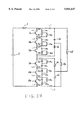
- FIG. 1 is a block diagram showing a construction of a part of a power conversion system according to a first embodiment of this invention
- FIG. 3 is a block diagram showing a construction of a part of a power conversion system according to a third embodiment of this invention.
- FIG. 5A is a block diagram showing a construction of a part of a power conversion system according to a fifth embodiment of this invention.
- FIG. 5C is a block diagram showing a construction of a part of a power conversion system according to a sixth embodiment of this invention.
- the current flowing to IGBT 5a is absorbed by capacitor 2a via diode 3a of the upper RCD snubber circuit so that high voltage and large current are not simultaneously applied to IGBT 5a when the current is cut OFF. Namely, as for the voltage applied to IGBT 5a, the dv/dt is suppressed when capacitor 2a is charged. Accordingly, high voltage and large current are not simultaneously applied to IGBT 5a and IGBT 5a will not be destructed. The charge stored in capacitor 2a is consumed through resistor 4a and IGBT 5a and the power is thus lost at the time of next turn-ON. Therefore, from the viewpoint of the power loss, it is better that the capacitance of capacitor 2a is rather small.
- the dv/dt is suppressed by the RCD snubber circuit and the overvoltage generated by the line inductance is suppressed by the clamp snubber circuit. Further, from the viewpoint of the power loss, it is sufficient for the capacitor of the RCD snubber circuit to suppress the dv/dt to such a level that the IGBT is not destructed, and thereforte, a very small capacitance is sufficient. Accordingly, as the capacitor of the RCD snubber circuit, a capacitor of a fixed small capacitance is usable, and even when it is completely charged or discharged, the snubber loss can be minimized.
- This embodiment is the same as the first embodiment in that the clamp snubber circuits are connected, and differs in that as the charge/discharge snubber circuits, RC snubber circuits are used instead of the RCD snubber circuits. That is, in FIG. 2, diodes 3a and 3d used in the embodiment shown in FIG. 1 are omitted. As a result of the use of the RC snubber circuits, the current to be charged in capacitor 2a is charged by way of resistor 4a. The capability of suppressing dv/dt in this embodiment becomes inferior to that of the RCD snubber circuit in the first embodiment.
- Capacitor 2a and resistor 4a should be set as described below. That is, the capacitance of capacitor 2a should be set at a value larger than a value to suppress the dv/dt so that IGBT 5a is not destructed, and the resistance of resistor 4a should be set at a value smaller than a value to suppress the dv/dt so that IGBT 5a is not destructed
- this embodiment has a merit in the following point when compared with the first embodiment. That is, in the first embodiment when the operation is started from the state where a voltage of DC power source 7 is E and both IGBTS 5a, 5b are OFF, the voltages of snubber capacitors 2a and 2c of the RCD snubber circuits become E/2, respectively. When either one of IGBTs 5a, 5b is turned ON, the snubber capacitor connected to the other IGBT is rapidly charged to E from E/2.
- the charging current is not able to suppress the di/dt because there is line inductance 6 only in the route of the charging current as an impedance component. If there is a possibility for destructing IGBTs 5a, 5b by the di/dt at the time of their turn-ON, it is necessary to add an anode reactor, etc. in order to increase the inductance thereby to suppress the di/dt. This will result in an increase of the power loss in the snubber circuit.
- resistors 4a, 4c are respectively connected to capacitors 2a, 2c in series in the RC snubber circuits, and therefore, it is necessary to provide an anode reactor for the reason of the above cause as in the first embodiment. Accordingly, it is possible to further reduce the power loss.
- This embodiment is the same as the first embodiment in that the clamp snubber circuits are connected and differs in that as the charge/discharge snubber circuit snubber circuits composed of only capacitors 2a, 2c are used instead of the RCD snubber circuits. That is, in FIG. 3, diodes 3a and 3d and resistors 4a, 4c used in the embodiment shown in FIG. 1 are omitted. As a result of the use of the snubber circuits composed of only capacitors 2a, 2c instead of the RCD snubber circuits or the RC snubber circuits, this embodiment differs from the first and second embodiments in the following points.
- FIG. 5A a power conversion system is constructed such that power devices are connected in series in the upper and lower arms, respectively, so as to provide a high voltage power conversion system.
- IGBTs 5a, 5b, capacitors 2a, 2c, diodes 3a, 3c and resistors 4a, 4a are used by three pieces, respectively, and they are discriminated by adding suffixes 1, 2 and 3 to their reference numerals, respectively.
- the clamp snubber circuits each of clamp snubber circuits is connected to one of the upper and lower arms, respectively, as in the first embodiment.
- FIG. 5B is a block diagram for explaining the action of the power conversion system shown in FIG. 5A.
- the charge/discharge snubber circuits (RCD snubber circuits) are provided near the respective IGBTs 5a1, 5a2, 5a3 and IGBTs 5b1, 5b2 and 5b3.
- the line inductances shown by reference numerals La1, La2, La3 and Lc1, Lc2, Lc3 in FIG. 5B of the charge/discharge snubber circuits are small.
- capacitors 2a1, 2a2, 2a3 or capacitors 2c1, 2c2, 2c3 in the charge/discharge snubber circuits are very small, the charged voltages of capacitors 2a1, 2a2, 2a3 or capacitors 2c1, 2c2, 2c3 becomes extremely high, with the result that IGBTs 5a1, 5a2, 5a3 or IGBTs 5b1, 5b2 and 5b3 may be destructed by the overvoltage.
- FIG. 5C a sixth embodiment is provided as shown in FIG. 5C.
- This embodiment is the same as the fifth embodiment except that anode reactors LAa and LAb are further provided in the upper and lower arms, respectively, as shown in FIG. 5C.
- the inductances of anode reactors LAa and LAb are determinded by the following expression:
- a power conversion system composed of a plurality of power devices having a large dv/dt withstand value which is capable of protecting the power devices from being destructed, reducing the power loss in snubber circuits when these power devices are turned OFF, and further suppressing the overvoltage of the arms individually, by suppressing the dv/dt and the overvoltage.
Landscapes
- Engineering & Computer Science (AREA)
- Power Engineering (AREA)
- Inverter Devices (AREA)
- Power Conversion In General (AREA)
Applications Claiming Priority (2)
| Application Number | Priority Date | Filing Date | Title |
|---|---|---|---|
| JP8-264973 | 1996-10-07 | ||
| JP26497396 | 1996-10-07 |
Publications (1)
| Publication Number | Publication Date |
|---|---|
| US5841647A true US5841647A (en) | 1998-11-24 |
Family
ID=17410790
Family Applications (1)
| Application Number | Title | Priority Date | Filing Date |
|---|---|---|---|
| US08/943,805 Expired - Lifetime US5841647A (en) | 1996-10-07 | 1997-10-03 | Power conversion system |
Country Status (4)
| Country | Link |
|---|---|
| US (1) | US5841647A (de) |
| EP (1) | EP0834982A3 (de) |
| KR (1) | KR100352860B1 (de) |
| CN (1) | CN1056481C (de) |
Cited By (11)
| Publication number | Priority date | Publication date | Assignee | Title |
|---|---|---|---|---|
| US6268990B1 (en) | 1998-06-26 | 2001-07-31 | Kabushiki Kaisha Toshiba | Semiconductor protection device and power converting system |
| US20040221247A1 (en) * | 2003-04-30 | 2004-11-04 | Andreev Alexandre E. | Method for generating tech-library for logic function |
| US20070030282A1 (en) * | 2005-05-24 | 2007-02-08 | Magnum Communications, Limited | System and method for defining attributes, decision rules, or both, for remote execution, claim set iv |
| US20090128454A1 (en) * | 2007-11-16 | 2009-05-21 | Jin-Ho Yang | Plasma display device, and driving apparatus and method thereof |
| US20130242617A1 (en) * | 2012-03-15 | 2013-09-19 | Huaguang Zhang | H-bridge micro inverter grid-connected device |
| CN103534920A (zh) * | 2011-05-02 | 2014-01-22 | 大金工业株式会社 | 电力转换电路及空调装置 |
| US8716986B2 (en) | 2010-05-07 | 2014-05-06 | Mitsubishi Electric Corporation | Power conversion circuit |
| US20160336733A1 (en) * | 2015-05-11 | 2016-11-17 | Infineon Technologies Ag | System and Method for a Multi-Phase Snubber Circuit |
| CN106364328A (zh) * | 2016-09-30 | 2017-02-01 | 新风光电子科技股份有限公司 | 制动能量吸收装置及其控制方法 |
| DE102011120841B4 (de) * | 2011-12-13 | 2017-08-10 | Jungheinrich Aktiengesellschaft | Wechselrichter mit Totzeitkorrektur sowie Verfahren zur Korrektur der Totzeit in einem Wechselrichter |
| CN109889028A (zh) * | 2019-03-29 | 2019-06-14 | 阳光电源股份有限公司 | 一种吸收电容预充电电路和尖峰电压吸收电路 |
Families Citing this family (9)
| Publication number | Priority date | Publication date | Assignee | Title |
|---|---|---|---|---|
| KR20000046000A (ko) * | 1998-12-31 | 2000-07-25 | 추호석 | 전기차 제어장치의 인버터 |
| JP5146011B2 (ja) * | 2008-02-28 | 2013-02-20 | ダイキン工業株式会社 | 直接形交流電力変換装置 |
| JP5117438B2 (ja) * | 2009-03-31 | 2013-01-16 | 住友重機械工業株式会社 | リフティングマグネット用電源回路 |
| JP5573884B2 (ja) * | 2012-04-25 | 2014-08-20 | 株式会社デンソー | 電力変換装置 |
| CN103066809B (zh) * | 2012-12-06 | 2015-04-29 | 国网智能电网研究院 | 一种应用于直接串联型igbt的改进型rcd缓冲电路 |
| CN105612687B (zh) * | 2013-06-26 | 2018-08-14 | 华为技术有限公司 | 一种光伏应用场景下基于三态开关单元概念的dc-dc升压变换器 |
| CN108667441B (zh) | 2017-03-31 | 2022-07-26 | 通用电气公司 | 功率半导体器件及其缓冲电路 |
| EP3963707A4 (de) * | 2019-05-01 | 2023-01-04 | Rompower Technology Holdings, LLC | Hocheffiziente passive klammer |
| US11996785B1 (en) | 2022-11-17 | 2024-05-28 | Rompower Technology Holdings, Llc | High efficiency AC-DC converter |
Citations (6)
| Publication number | Priority date | Publication date | Assignee | Title |
|---|---|---|---|---|
| US4697230A (en) * | 1986-06-23 | 1987-09-29 | Westinghouse Electric Corp. | AC power supplied static switching apparatus having energy recovery capability |
| US4926306A (en) * | 1988-08-12 | 1990-05-15 | Hitachi, Ltd. | Electric power converter |
| US4937725A (en) * | 1989-06-19 | 1990-06-26 | Sundstrand Corporation | Circuit for eliminating snubber current noise in the sense circuit of an H-bridge inverter |
| US5077651A (en) * | 1989-09-20 | 1991-12-31 | Fuji Electric Co., Ltd. | Snubber circuit of power converter |
| US5424937A (en) * | 1992-06-10 | 1995-06-13 | Hitachi, Ltd. | Gate drive power source for electric power converter |
| US5579215A (en) * | 1994-09-08 | 1996-11-26 | Kabushiki Kaisha Toshiba | Power conversion device with snubber energy regenerating circuit |
Family Cites Families (2)
| Publication number | Priority date | Publication date | Assignee | Title |
|---|---|---|---|---|
| DE2724741C3 (de) * | 1977-06-01 | 1980-02-21 | Siemens Ag, 1000 Berlin Und 8000 Muenchen | Schutzbeschaltung für jeweils ein Stromrichterventil |
| SE9500761D0 (sv) * | 1995-03-02 | 1995-03-02 | Abb Research Ltd | Skyddskrets för seriekopplade krafthalvledare |
-
1997
- 1997-10-03 US US08/943,805 patent/US5841647A/en not_active Expired - Lifetime
- 1997-10-06 EP EP97307897A patent/EP0834982A3/de not_active Withdrawn
- 1997-10-07 KR KR1019970051423A patent/KR100352860B1/ko not_active Expired - Fee Related
- 1997-10-07 CN CN97120576A patent/CN1056481C/zh not_active Expired - Fee Related
Patent Citations (6)
| Publication number | Priority date | Publication date | Assignee | Title |
|---|---|---|---|---|
| US4697230A (en) * | 1986-06-23 | 1987-09-29 | Westinghouse Electric Corp. | AC power supplied static switching apparatus having energy recovery capability |
| US4926306A (en) * | 1988-08-12 | 1990-05-15 | Hitachi, Ltd. | Electric power converter |
| US4937725A (en) * | 1989-06-19 | 1990-06-26 | Sundstrand Corporation | Circuit for eliminating snubber current noise in the sense circuit of an H-bridge inverter |
| US5077651A (en) * | 1989-09-20 | 1991-12-31 | Fuji Electric Co., Ltd. | Snubber circuit of power converter |
| US5424937A (en) * | 1992-06-10 | 1995-06-13 | Hitachi, Ltd. | Gate drive power source for electric power converter |
| US5579215A (en) * | 1994-09-08 | 1996-11-26 | Kabushiki Kaisha Toshiba | Power conversion device with snubber energy regenerating circuit |
Cited By (18)
| Publication number | Priority date | Publication date | Assignee | Title |
|---|---|---|---|---|
| US6268990B1 (en) | 1998-06-26 | 2001-07-31 | Kabushiki Kaisha Toshiba | Semiconductor protection device and power converting system |
| US20040221247A1 (en) * | 2003-04-30 | 2004-11-04 | Andreev Alexandre E. | Method for generating tech-library for logic function |
| US7062726B2 (en) * | 2003-04-30 | 2006-06-13 | Lsi Logic Corporation | Method for generating tech-library for logic function |
| US20070030282A1 (en) * | 2005-05-24 | 2007-02-08 | Magnum Communications, Limited | System and method for defining attributes, decision rules, or both, for remote execution, claim set iv |
| US7860782B2 (en) * | 2005-05-24 | 2010-12-28 | Magnum Communications, Limited | System and method for defining attributes, decision rules, or both, for remote execution, claim set IV |
| US20090128454A1 (en) * | 2007-11-16 | 2009-05-21 | Jin-Ho Yang | Plasma display device, and driving apparatus and method thereof |
| US8716986B2 (en) | 2010-05-07 | 2014-05-06 | Mitsubishi Electric Corporation | Power conversion circuit |
| US9065357B2 (en) | 2010-05-07 | 2015-06-23 | Mitsubishi Electric Corporation | Power conversion circuit |
| CN103534920A (zh) * | 2011-05-02 | 2014-01-22 | 大金工业株式会社 | 电力转换电路及空调装置 |
| CN103534920B (zh) * | 2011-05-02 | 2016-05-11 | 大金工业株式会社 | 电力变换电路及空调装置 |
| DE102011120841B4 (de) * | 2011-12-13 | 2017-08-10 | Jungheinrich Aktiengesellschaft | Wechselrichter mit Totzeitkorrektur sowie Verfahren zur Korrektur der Totzeit in einem Wechselrichter |
| US20130242617A1 (en) * | 2012-03-15 | 2013-09-19 | Huaguang Zhang | H-bridge micro inverter grid-connected device |
| US9190920B2 (en) * | 2012-03-15 | 2015-11-17 | Northeastern University | H-bridge micro inverter grid-connected device |
| US20160336733A1 (en) * | 2015-05-11 | 2016-11-17 | Infineon Technologies Ag | System and Method for a Multi-Phase Snubber Circuit |
| US9768607B2 (en) * | 2015-05-11 | 2017-09-19 | Infineon Technologies Ag | System and method for a multi-phase snubber circuit |
| CN106364328A (zh) * | 2016-09-30 | 2017-02-01 | 新风光电子科技股份有限公司 | 制动能量吸收装置及其控制方法 |
| CN106364328B (zh) * | 2016-09-30 | 2019-04-02 | 新风光电子科技股份有限公司 | 制动能量吸收装置及其控制方法 |
| CN109889028A (zh) * | 2019-03-29 | 2019-06-14 | 阳光电源股份有限公司 | 一种吸收电容预充电电路和尖峰电压吸收电路 |
Also Published As
| Publication number | Publication date |
|---|---|
| CN1182972A (zh) | 1998-05-27 |
| KR19980032619A (ko) | 1998-07-25 |
| KR100352860B1 (ko) | 2002-12-26 |
| EP0834982A2 (de) | 1998-04-08 |
| EP0834982A3 (de) | 1999-02-10 |
| CN1056481C (zh) | 2000-09-13 |
Similar Documents
| Publication | Publication Date | Title |
|---|---|---|
| US5841647A (en) | Power conversion system | |
| US5077651A (en) | Snubber circuit of power converter | |
| US6043636A (en) | Voltage transient suppression | |
| US11451135B2 (en) | Multilevel port under-voltage protection circuit with flying capacitor | |
| JP3262495B2 (ja) | マルチレベルインバータ | |
| US4947311A (en) | Electrical power conversion circuit | |
| EP3574576B1 (de) | Schutzanordnung für ein submodul eines mmc-hvdc | |
| JP3133166B2 (ja) | ゲート電力供給回路 | |
| JPH07312878A (ja) | 3レベルインバータのスナバ回路 | |
| JPH07250484A (ja) | 系統連系用高電圧自励変換装置 | |
| US4855887A (en) | Current and frequency converter having means to reduce switching losses | |
| JPH10174424A (ja) | 電力変換装置 | |
| JP4765018B2 (ja) | 電力変換装置 | |
| JP2790600B2 (ja) | 電力変換装置 | |
| NL2028254B1 (en) | Electrical converter with overvoltage protection circuit | |
| JP2861169B2 (ja) | 電力変換装置のスナバ回路 | |
| Han et al. | Soft-switching characterization of 3.3 kV reverse-blocking SiC devices | |
| Knöll | High-current transistor choppers | |
| JP3321203B2 (ja) | 絶縁型スイッチング回路、シールド機能を持つ絶縁型スイッチング回路および絶縁型スイッチング回路 | |
| JPS586078A (ja) | インバ−タ | |
| JP2002044934A (ja) | 半導体電力変換装置 | |
| JPH07194131A (ja) | 3レベルインバータ装置 | |
| JP7147998B2 (ja) | 半導体振動抑制回路 | |
| JPH04289778A (ja) | 電力変換器のスナバ回路 | |
| JPH0336221Y2 (de) |
Legal Events
| Date | Code | Title | Description |
|---|---|---|---|
| AS | Assignment |
Owner name: KABUSHIKI KAISHA TOSHIBA, JAPAN Free format text: ASSIGNMENT OF ASSIGNORS INTEREST;ASSIGNOR:HOSHI, KIMIHIRO;REEL/FRAME:009129/0300 Effective date: 19980323 |
|
| STCF | Information on status: patent grant |
Free format text: PATENTED CASE |
|
| FPAY | Fee payment |
Year of fee payment: 4 |
|
| FPAY | Fee payment |
Year of fee payment: 8 |
|
| FEPP | Fee payment procedure |
Free format text: PAYER NUMBER DE-ASSIGNED (ORIGINAL EVENT CODE: RMPN); ENTITY STATUS OF PATENT OWNER: LARGE ENTITY Free format text: PAYOR NUMBER ASSIGNED (ORIGINAL EVENT CODE: ASPN); ENTITY STATUS OF PATENT OWNER: LARGE ENTITY |
|
| FPAY | Fee payment |
Year of fee payment: 12 |