US6801018B2 - Buffer circuit - Google Patents
Buffer circuit Download PDFInfo
- Publication number
- US6801018B2 US6801018B2 US10/297,268 US29726802A US6801018B2 US 6801018 B2 US6801018 B2 US 6801018B2 US 29726802 A US29726802 A US 29726802A US 6801018 B2 US6801018 B2 US 6801018B2
- Authority
- US
- United States
- Prior art keywords
- voltage
- load
- buffer
- capacitor
- coupled
- Prior art date
- Legal status (The legal status is an assumption and is not a legal conclusion. Google has not performed a legal analysis and makes no representation as to the accuracy of the status listed.)
- Expired - Fee Related, expires
Links
Images


Classifications
-
- H—ELECTRICITY
- H02—GENERATION; CONVERSION OR DISTRIBUTION OF ELECTRIC POWER
- H02M—APPARATUS FOR CONVERSION BETWEEN AC AND AC, BETWEEN AC AND DC, OR BETWEEN DC AND DC, AND FOR USE WITH MAINS OR SIMILAR POWER SUPPLY SYSTEMS; CONVERSION OF DC OR AC INPUT POWER INTO SURGE OUTPUT POWER; CONTROL OR REGULATION THEREOF
- H02M3/00—Conversion of DC power input into DC power output
- H02M3/02—Conversion of DC power input into DC power output without intermediate conversion into AC
- H02M3/04—Conversion of DC power input into DC power output without intermediate conversion into AC by static converters
- H02M3/10—Conversion of DC power input into DC power output without intermediate conversion into AC by static converters using discharge tubes with control electrode or semiconductor devices with control electrode
- H02M3/145—Conversion of DC power input into DC power output without intermediate conversion into AC by static converters using discharge tubes with control electrode or semiconductor devices with control electrode using devices of a triode or transistor type requiring continuous application of a control signal
- H02M3/155—Conversion of DC power input into DC power output without intermediate conversion into AC by static converters using discharge tubes with control electrode or semiconductor devices with control electrode using devices of a triode or transistor type requiring continuous application of a control signal using semiconductor devices only
- H02M3/156—Conversion of DC power input into DC power output without intermediate conversion into AC by static converters using discharge tubes with control electrode or semiconductor devices with control electrode using devices of a triode or transistor type requiring continuous application of a control signal using semiconductor devices only with automatic control of output voltage or current, e.g. switching regulators
- H02M3/158—Conversion of DC power input into DC power output without intermediate conversion into AC by static converters using discharge tubes with control electrode or semiconductor devices with control electrode using devices of a triode or transistor type requiring continuous application of a control signal using semiconductor devices only with automatic control of output voltage or current, e.g. switching regulators including plural semiconductor devices as final control devices for a single load
- H02M3/1582—Buck-boost converters
Definitions
- the invention concerns a buffer circuit for a load to be supplied by a supply DC voltage, with a buffer capacitor, which can be charged to a voltage by a charging circuit, which voltage is higher than the supply DC voltage and which can be brought in at the time of dips in the supply voltage for supply of the load by a discharging circuit.
- Buffer circuits are used to buffer a supply DC voltage, in order to be able to continue to operate devices temporarily in the event of voltage dips, e.g., in power grid voltage. This is, for example, important with electronic devices to avoid data losses without having to resort to the very expensive solution of uninterruptible power supplies that are fed by accumulators.
- a problem which occurs with all buffer circuits of the art in question is the low energy that can be stored in a capacitor compared to accumulators, whereby this energy increases in direct proportion with capacitance but quadratically relative to the charging voltage. To save cost and volume, an increase of the buffer energy by increasing the capacitor voltage is naturally advisable.
- buffer capacitors takes place in many cases via a resistor—which, however, is associated with high losses—or via a current source circuit. If a limitation of the voltage on the buffer capacitor is necessary or desired, this can be handled, for instance, by a Zener diode connected in parallel.
- Known discharging circuits consist of a switch controlled by a trigger circuit and a limiting resistor, whereby the voltage must be limited possibly by a parallel regulator, a Zener diode, or by reopening the switch. In this process, in any case, half the stored buffer energy is lost as Joule heat.
- DD 223,302 A1 presents a buffer circuit of the art in question, wherein an additional winding with a rectifier connected downstream is used on the transformer of a switching power supply to charge the buffer capacitor.
- the load is fed from a secondary winding with a rectifier connected downstream, and the actual supply voltage is coupled to the primary winding of the transformer via a controlled switch.
- JP 10 062456 A discloses a voltage monitoring circuit that delivers a reset signal to a CPU when the supply voltage of the CPU drops below a predefinable minimum.
- DE 38 05 256 A1 discloses a circuit for the emergency power supply of a consuming device in a motor vehicle, whereby a storage capacitor is charged via a step-up controller.
- a selected consuming device is supplied via a regulator from the battery voltage; whereas, in the event of failure of the battery voltage, the capacitor is connected via an additional longitudinal regulator to the input of the aforementioned regulator and the selected consuming device is supplied.
- a similar circuit is presented in DE 195 42 085 A1.
- a selected consuming device that represents only a fraction of the possible total load of the auto battery is temporarily supplied in the event of a failure.
- the supply again occurs from a capacitor which is charged by a step-up controller, whereby the voltage is fed to the selected consuming device via a stabilizer.
- One object of the invention is to provide a buffer circuit that achieves, on the one hand, high stored energy with relatively low cost and small structural volume, and can, on the other, be connected directly to the load to be buffered, i.e., merely with a two wire connection.
- One object of the invention is to provide a buffer circuit that achieves high stored energy with relatively low cost and small structural volume.
- a buffer circuit of the type mentioned in the introduction that is characterized according to the invention by a step-down controller, whose input is coupled to the buffer capacitor and whose output is coupled to the load, and a trigger circuit, which is configured to activate the step-down controller in the event of dropout of the voltage at the load.
- the buffer circuit according to the invention offers not only the advantages of low cost and minimal structural volume with maximum stored energy, but it also can be located in an external device that can be used as an add-on to an already existing power supply.
- the charging circuit is a step-up controller whose input is coupled to the load and whose output is coupled to the buffer capacitor, it is possible, on the one hand, to avoid the losses inherent to a charging resistor and, on the other, not to have to rely on the level of the supply voltage or an auxiliary voltage, generated, for instance, by voltage doubling.
- the trigger circuit is configured to deliver switching pulses to the step-down controller.
- the potential segregation means is a transformer via which the output of the trigger circuit is connected to the step-down controller.
- the step-up controller to have a first controlled switch, via which a first inductance can be periodically connected to the load voltage, plus a first capacitor coupled in parallel to the load, as well as a first diode leading to the buffer capacitor from the connection of the first inductance with the first switch.
- the step-down controller has a second controlled switch via which the voltage on the buffer capacitor can be periodically connected to the load in series with a second inductance, to which load a second capacitor is coupled in parallel, and the series connection of the second inductance with the second capacitor is jumpered by a backflow diode.
- FIG. 1 the invention using a schematic diagram
- FIG. 2 a circuit according to the invention, detailed, yet restricted to the essentials.
- an input voltage U E e.g., power grid AC voltage of 230 volts is converted in a switching converter SWA into a supply DC voltage U V , e.g., 24 volts, that is connected to the terminals of a load LAS.
- the load LAS may, in principle, be any consuming device; however, in the context of the invention a failure-critical device is primarily considered.
- a step-up controller HSS is connected by its input to the load terminals, whereas a buffer capacitor C p is coupled to the output of the step-up controller.
- the load voltage which corresponds, with a properly operating switching converter SWA, to its output voltage, i.e., the supply DC voltage U V , is coupled to the input of the step-up controller HSS.
- Step-up controllers are known to the person skilled in the art in many implementations. These are switching converters that convert a first DC voltage, in this case U V , into a second DC voltage that is greater than the first voltage.
- the second DC voltage is, in the present case, the voltage U H on the buffer capacitor C p .
- the energy values thus differ by a factor of approximately 35.
- the buffer capacitor may also be charged via a charging resistor by a voltage that is higher than the supply voltage. This can be the case, in particular, if such a higher voltage, which actually serves a different purpose, is present at a switching converter output, or if the higher DC voltage can be obtained from an AC voltage via a simple voltage doubling circuit, e.g., with two diodes and capacitors.
- the voltage U H of the buffer capacitor C p is coupled to the input of a step-down controller TSS, whose output is coupled to the load terminals a, b, and whose role it is, when necessary, to convert the voltage U H on the buffer capacitor C p to the voltage U V , i.e., the necessary load voltage.
- Step-down controllers are also known to the person skilled in the art in many variants. They should drop a first DC voltage, in this case U H , to a second, lower DC voltage, in this case to U V .
- a trigger circuit TRI monitors the load voltage U V , e.g., by comparison with a reference voltage and is configured to feed the step-down controller TSS an activation signal sa as soon as the load voltage U V drops to a specific value, e.g., 0.7 U V .
- the trigger circuit TRI can, for instance, generate the switching pulse necessary for the operation of the step-down controller TSS and deliver it to the step-down controller TSS.
- the activation signal sa is a pulse sequence with a specific pulse duty factor.
- the switching pulses may also be generated in the step-down controller TSS itself and released via the activation signal s a .
- the trigger circuit TRI activates the step-down controller TSS, which now supplies the load LAS with the correct supply voltage from the energy of the buffer capacitor C p until either the actual supply voltage U V has again reached a certain minimum value or until the voltage of the buffer capacitor C p has dropped to a value at which the step-down controller TSS no longer operates.
- the trigger circuit TRI must cancel the activation signal sa as soon as the supply voltage U V has reached its normal value.
- the trigger circuit TRI may, as described here, monitor the voltage on the load LAS directly, but the voltage may also be monitored on the input side of a switching converter.
- the trigger circuit can at least sometimes also be housed in a switching converter, as depicted in FIG. 1 by a broken line, a trigger block TRI′, and a signal s′ a .
- the block “TRI” in FIG. 1 could even be omitted.
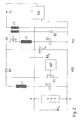
- FIG. 2 depicts in greater detail a practical embodiment of the invention; however, details unnecessary for the explanation of the invention or already commonly known to the person skilled in the art are omitted.
- the load LAS is supplied by a DC voltage U V , which may, for example, be delivered by a switching converter.
- a buffer circuit according to the invention is connected to the terminals a, b of the load LAS, whereby it should be clear that the buffer circuit can be incorporated even after the fact into an existing power supply or can be connected to the load via a cable as an add-on device.
- the step-up controller HSS consists of a capacitor C 1 , an inductance L 1 , a first controlled switch V 1 , along with a control circuit AST and a first diode D 1 , whereby the capacitor C 1 is coupled in parallel to the load LAS and the series connection of the inductance L 1 and of the switch V 1 is coupled parallel thereto. From the connection point of the inductance with the switch V 1 , the diode D 1 leads to the buffer capacitor C p .
- the control circuit AST delivers, in known fashion, a pulse sequence with a pulse duty factor that is constant in the simplest case or is variable, for instance, for the regulation of the voltage U H on the buffer capacitor C p depending on this voltage.
- the step-down controller TSS is, when necessary, supplied by this voltage U H , which can be significantly higher than the voltage U V on the load LAS.
- the step-down controller has, coupled in series to the buffer capacitor C p , a second controlled switch V 2 , a second inductance L 2 , and a second capacitor C 2 , whereby a backflow diode D 2 is coupled in parallel to the series connection inductance L 2 —capacitor C 2 .
- the second controlled switch V 2 is also supplied by pulses with constant or optionally variable pulse width. In the present case, the pulses are generated in the trigger circuit TRI, to which the load voltage U V is coupled, such that this can be monitored.
- the trigger circuit TRI connects, for activation of the step-down controller, the pulse sequence as activation signal s a to the control input of the second switch V 2 , whereby a transformer T 2 serves in this case for potential segregation.
- Other means e.g., an optical coupler, even in a different location, e.g., on the input side, could also be used for potential segregation.
- the step-down controller TSS now reduces the high voltage U H on the buffer capacitor C p to the value required by the load LAS and supplies the load LAS until either the load voltage has returned to the supply voltage or the energy of the buffer capacitor has been exhausted.
- the buffer capacitor is dimensioned such that the load can be supplied for a period of time that is adequate, for example, to shut down a system, so that no data loss occurs.
Landscapes
- Engineering & Computer Science (AREA)
- Power Engineering (AREA)
- Dc-Dc Converters (AREA)
- Stand-By Power Supply Arrangements (AREA)
Applications Claiming Priority (4)
| Application Number | Priority Date | Filing Date | Title |
|---|---|---|---|
| AT0096600A AT411412B (de) | 2000-05-31 | 2000-05-31 | Pufferschaltung |
| ATA966/2000 | 2000-05-31 | ||
| AT966/2000 | 2000-05-31 | ||
| PCT/AT2001/000176 WO2001093411A1 (de) | 2000-05-31 | 2001-05-30 | Pufferschaltung |
Publications (2)
| Publication Number | Publication Date |
|---|---|
| US20040012988A1 US20040012988A1 (en) | 2004-01-22 |
| US6801018B2 true US6801018B2 (en) | 2004-10-05 |
Family
ID=3683621
Family Applications (1)
| Application Number | Title | Priority Date | Filing Date |
|---|---|---|---|
| US10/297,268 Expired - Fee Related US6801018B2 (en) | 2000-05-31 | 2001-05-30 | Buffer circuit |
Country Status (4)
| Country | Link |
|---|---|
| US (1) | US6801018B2 (de) |
| EP (1) | EP1287605A1 (de) |
| AT (1) | AT411412B (de) |
| WO (1) | WO2001093411A1 (de) |
Cited By (2)
| Publication number | Priority date | Publication date | Assignee | Title |
|---|---|---|---|---|
| US20080074078A1 (en) * | 2006-09-26 | 2008-03-27 | Tai-Her Yang | Circuit installation capable of full voltage activation, division voltage operation and delayed breaking |
| US20080264915A1 (en) * | 2007-04-30 | 2008-10-30 | Illinois Tool Works Inc. | Welding power source with automatic variable high frequency |
Families Citing this family (6)
| Publication number | Priority date | Publication date | Assignee | Title |
|---|---|---|---|---|
| DE10308411A1 (de) | 2003-02-27 | 2004-09-23 | Bosch Rexroth Ag | Gleichstromwandlerschaltung |
| DE102005011519B4 (de) * | 2005-03-10 | 2012-08-30 | Secop Gmbh | Verfahren zur Steuerung einer Gleichspannungsquelle und Spannungsversorgungsvorrichtung |
| US7844304B1 (en) * | 2005-10-27 | 2010-11-30 | Rockwell Collins, Inc. | Method of filtering low frequency components from power lines |
| US7636260B2 (en) | 2007-06-25 | 2009-12-22 | Sandisk Corporation | Method for operating non-volatile storage with individually controllable shield plates between storage elements |
| US7781286B2 (en) | 2007-06-25 | 2010-08-24 | Sandisk Corporation | Method for fabricating non-volatile storage with individually controllable shield plates between storage elements |
| DE102009002202A1 (de) | 2009-04-06 | 2010-10-14 | Beckhoff Automation Gmbh | Schaltung und Verfahren zur unterbrechungsfreien Stromversorgung elektronischer Baugruppen |
Citations (6)
| Publication number | Priority date | Publication date | Assignee | Title |
|---|---|---|---|---|
| US4197582A (en) * | 1978-03-31 | 1980-04-08 | Westinghouse Electric Corp. | Auxiliary power supply and timer arrangement for time registering multifunctional electric energy meters |
| DE3805256A1 (de) | 1988-02-19 | 1989-08-31 | Siemens Ag | Reserveschaltung zur notstromversorgung eines verbrauchers in einem fahrzeug |
| DE19542085A1 (de) | 1994-12-30 | 1996-07-04 | Bosch Gmbh Robert | Elektronisches Gerät |
| EP0798840A2 (de) | 1996-03-27 | 1997-10-01 | Siemens Aktiengesellschaft | Batterie-Stromversorgung |
| US5714863A (en) | 1996-02-20 | 1998-02-03 | Motorola, Inc. | Circuit for enhancing power delivery of an energy source |
| US6366070B1 (en) * | 2001-07-12 | 2002-04-02 | Analog Devices, Inc. | Switching voltage regulator with dual modulation control scheme |
Family Cites Families (2)
| Publication number | Priority date | Publication date | Assignee | Title |
|---|---|---|---|---|
| DD223302A1 (de) * | 1983-12-09 | 1985-06-05 | Inst Prueffeld Elekt | Schaltungsanordnung zum puffern von umrichtern |
| JP3706207B2 (ja) * | 1996-08-22 | 2005-10-12 | 沖電気工業株式会社 | 電圧監視回路 |
-
2000
- 2000-05-31 AT AT0096600A patent/AT411412B/de not_active IP Right Cessation
-
2001
- 2001-05-30 EP EP01937846A patent/EP1287605A1/de not_active Ceased
- 2001-05-30 US US10/297,268 patent/US6801018B2/en not_active Expired - Fee Related
- 2001-05-30 WO PCT/AT2001/000176 patent/WO2001093411A1/de not_active Ceased
Patent Citations (8)
| Publication number | Priority date | Publication date | Assignee | Title |
|---|---|---|---|---|
| US4197582A (en) * | 1978-03-31 | 1980-04-08 | Westinghouse Electric Corp. | Auxiliary power supply and timer arrangement for time registering multifunctional electric energy meters |
| DE3805256A1 (de) | 1988-02-19 | 1989-08-31 | Siemens Ag | Reserveschaltung zur notstromversorgung eines verbrauchers in einem fahrzeug |
| DE19542085A1 (de) | 1994-12-30 | 1996-07-04 | Bosch Gmbh Robert | Elektronisches Gerät |
| US5714863A (en) | 1996-02-20 | 1998-02-03 | Motorola, Inc. | Circuit for enhancing power delivery of an energy source |
| EP0798840A2 (de) | 1996-03-27 | 1997-10-01 | Siemens Aktiengesellschaft | Batterie-Stromversorgung |
| EP0798840A3 (de) | 1996-03-27 | 1998-06-03 | Siemens Aktiengesellschaft | Batterie-Stromversorgung |
| EP0798840B1 (de) | 1996-03-27 | 2002-01-30 | Siemens Aktiengesellschaft | Batterie-Stromversorgung |
| US6366070B1 (en) * | 2001-07-12 | 2002-04-02 | Analog Devices, Inc. | Switching voltage regulator with dual modulation control scheme |
Non-Patent Citations (2)
| Title |
|---|
| International Preliminary Examination Report of PCT/AT01/00176, dated Apr. 9, 2002. |
| International Search Report of PCT/AT01/00176, dated Oct. 11, 2001. |
Cited By (8)
| Publication number | Priority date | Publication date | Assignee | Title |
|---|---|---|---|---|
| US20080074078A1 (en) * | 2006-09-26 | 2008-03-27 | Tai-Her Yang | Circuit installation capable of full voltage activation, division voltage operation and delayed breaking |
| US7839105B2 (en) * | 2006-09-26 | 2010-11-23 | Tai-Her Yang | Circuit installation capable of full voltage activation, division voltage operation and delayed breaking |
| US20110031818A1 (en) * | 2006-09-26 | 2011-02-10 | Tai-Her Yang | Circuit installation capable of full voltage activation, division voltage operation and delayed breaking |
| US7911164B2 (en) * | 2006-09-26 | 2011-03-22 | Tai-Her Yang | Circuit installation capable of full voltage activation, division voltage operation and delayed breaking |
| US20080264915A1 (en) * | 2007-04-30 | 2008-10-30 | Illinois Tool Works Inc. | Welding power source with automatic variable high frequency |
| US9108263B2 (en) | 2007-04-30 | 2015-08-18 | Illinois Tool Works Inc. | Welding power source with automatic variable high frequency |
| TWI470397B (zh) * | 2007-10-08 | 2015-01-21 | 楊泰和 | 全壓啟動分壓運作及延遲斷電電路裝置 |
| KR101565160B1 (ko) | 2007-10-08 | 2015-11-02 | 양태허 | 전압 기동 분압 작동 및 회로 중단 지연 장치 |
Also Published As
| Publication number | Publication date |
|---|---|
| US20040012988A1 (en) | 2004-01-22 |
| ATA9662000A (de) | 2003-05-15 |
| AT411412B (de) | 2003-12-29 |
| EP1287605A1 (de) | 2003-03-05 |
| WO2001093411A1 (de) | 2001-12-06 |
Similar Documents
| Publication | Publication Date | Title |
|---|---|---|
| US5822200A (en) | Low level, high efficiency DC/DC converter | |
| US7042178B2 (en) | Motor driving apparatus | |
| EP2658081B1 (de) | System und Verfahren zur Versorgung einer Last mit Stillstandsleistung | |
| JP3676384B2 (ja) | 発電機用励磁装置 | |
| US10948934B1 (en) | Voltage regulator with piecewise linear loadlines | |
| JPS59144369A (ja) | 信号コンバ−タ装置 | |
| EP3447892B1 (de) | Stromversorgungssystem | |
| US6816392B2 (en) | Overcurrent output protecting circuit and constant-voltage switching power supply incorporating the same | |
| US20240149811A1 (en) | Power supply control device | |
| US6801018B2 (en) | Buffer circuit | |
| US20130264879A1 (en) | Low power consumption backup power system | |
| JP2004304987A (ja) | 多出力dc−dcコンバータ | |
| US6879140B2 (en) | Power holdup circuit | |
| JPH07123609A (ja) | 燃料電池給電システム | |
| KR101538017B1 (ko) | 속응성을 향상된 비절연 멀티페이즈형 dc-dc 컨버터 및 그 구동 방법 | |
| US12261477B2 (en) | Backup power supply device and method for controlling backup power supply device | |
| US5877614A (en) | Electronic switch-mode power supply | |
| US11817767B2 (en) | Control power for submodules of a MMC converter | |
| US6665199B2 (en) | Device supplied with current of limited strength | |
| KR19990063794A (ko) | 소모기에 의존하지 않고 적어도 일시적으로 능동 부하를 갖는고정 사이클 전원 회로 | |
| JPH09261855A (ja) | 電源装置 | |
| KR101893687B1 (ko) | 무정전 직류전원장치 | |
| JP2800078B2 (ja) | 直流無停電電源システム | |
| KR102144076B1 (ko) | 에너지 회생-저장-복원 기능이 가능한 모터 구동 시스템 | |
| JP2000152519A (ja) | 瞬時電圧低下補償装置の充電方法 |
Legal Events
| Date | Code | Title | Description |
|---|---|---|---|
| AS | Assignment |
Owner name: SIEMENS AG OSTERREICH, AUSTRIA Free format text: ASSIGNMENT OF ASSIGNORS INTEREST;ASSIGNORS:KRANISTER, ANDREAS;WEINMEIER, HARALD;REEL/FRAME:014441/0214;SIGNING DATES FROM 20021119 TO 20021127 |
|
| FPAY | Fee payment |
Year of fee payment: 4 |
|
| AS | Assignment |
Owner name: SIEMENS AKTIENGESELLSCHAFT, GERMANY Free format text: ASSIGNMENT OF ASSIGNORS INTEREST;ASSIGNOR:SIEMENS AKTIENGESELLSCHAFT OSTERREICH;REEL/FRAME:025026/0796 Effective date: 20100910 |
|
| FPAY | Fee payment |
Year of fee payment: 8 |
|
| REMI | Maintenance fee reminder mailed | ||
| LAPS | Lapse for failure to pay maintenance fees | ||
| STCH | Information on status: patent discontinuation |
Free format text: PATENT EXPIRED DUE TO NONPAYMENT OF MAINTENANCE FEES UNDER 37 CFR 1.362 |
|
| STCH | Information on status: patent discontinuation |
Free format text: PATENT EXPIRED DUE TO NONPAYMENT OF MAINTENANCE FEES UNDER 37 CFR 1.362 |
|
| FP | Lapsed due to failure to pay maintenance fee |
Effective date: 20161005 |