US7812343B2 - Multilayer composite body having an electronic function - Google Patents
Multilayer composite body having an electronic function Download PDFInfo
- Publication number
- US7812343B2 US7812343B2 US11/911,429 US91142906A US7812343B2 US 7812343 B2 US7812343 B2 US 7812343B2 US 91142906 A US91142906 A US 91142906A US 7812343 B2 US7812343 B2 US 7812343B2
- Authority
- US
- United States
- Prior art keywords
- components
- layer
- composite body
- multilayer composite
- electrodes
- Prior art date
- Legal status (The legal status is an assumption and is not a legal conclusion. Google has not performed a legal analysis and makes no representation as to the accuracy of the status listed.)
- Expired - Fee Related, expires
Links
Images



Classifications
-
- H—ELECTRICITY
- H05—ELECTRIC TECHNIQUES NOT OTHERWISE PROVIDED FOR
- H05K—PRINTED CIRCUITS; CASINGS OR CONSTRUCTIONAL DETAILS OF ELECTRIC APPARATUS; MANUFACTURE OF ASSEMBLAGES OF ELECTRICAL COMPONENTS
- H05K1/00—Printed circuits
- H05K1/16—Printed circuits incorporating printed electric components, e.g. printed resistors, capacitors or inductors
-
- H—ELECTRICITY
- H10—SEMICONDUCTOR DEVICES; ELECTRIC SOLID-STATE DEVICES NOT OTHERWISE PROVIDED FOR
- H10P—GENERIC PROCESSES OR APPARATUS FOR THE MANUFACTURE OR TREATMENT OF DEVICES COVERED BY CLASS H10
- H10P10/00—Bonding of wafers, substrates or parts of devices
-
- G—PHYSICS
- G06—COMPUTING OR CALCULATING; COUNTING
- G06K—GRAPHICAL DATA READING; PRESENTATION OF DATA; RECORD CARRIERS; HANDLING RECORD CARRIERS
- G06K19/00—Record carriers for use with machines and with at least a part designed to carry digital markings
- G06K19/06—Record carriers for use with machines and with at least a part designed to carry digital markings characterised by the kind of the digital marking, e.g. shape, nature, code
- G06K19/067—Record carriers with conductive marks, printed circuits or semiconductor circuit elements, e.g. credit or identity cards also with resonating or responding marks without active components
- G06K19/07—Record carriers with conductive marks, printed circuits or semiconductor circuit elements, e.g. credit or identity cards also with resonating or responding marks without active components with integrated circuit chips
- G06K19/077—Constructional details, e.g. mounting of circuits in the carrier
- G06K19/07718—Constructional details, e.g. mounting of circuits in the carrier the record carrier being manufactured in a continuous process, e.g. using endless rolls
-
- G—PHYSICS
- G06—COMPUTING OR CALCULATING; COUNTING
- G06K—GRAPHICAL DATA READING; PRESENTATION OF DATA; RECORD CARRIERS; HANDLING RECORD CARRIERS
- G06K19/00—Record carriers for use with machines and with at least a part designed to carry digital markings
- G06K19/06—Record carriers for use with machines and with at least a part designed to carry digital markings characterised by the kind of the digital marking, e.g. shape, nature, code
- G06K19/067—Record carriers with conductive marks, printed circuits or semiconductor circuit elements, e.g. credit or identity cards also with resonating or responding marks without active components
- G06K19/07—Record carriers with conductive marks, printed circuits or semiconductor circuit elements, e.g. credit or identity cards also with resonating or responding marks without active components with integrated circuit chips
- G06K19/077—Constructional details, e.g. mounting of circuits in the carrier
- G06K19/07749—Constructional details, e.g. mounting of circuits in the carrier the record carrier being capable of non-contact communication, e.g. constructional details of the antenna of a non-contact smart card
-
- H—ELECTRICITY
- H10—SEMICONDUCTOR DEVICES; ELECTRIC SOLID-STATE DEVICES NOT OTHERWISE PROVIDED FOR
- H10D—INORGANIC ELECTRIC SEMICONDUCTOR DEVICES
- H10D64/00—Electrodes of devices having potential barriers
- H10D64/01—Manufacture or treatment
- H10D64/011—Manufacture or treatment of electrodes ohmically coupled to a semiconductor
-
- H—ELECTRICITY
- H10—SEMICONDUCTOR DEVICES; ELECTRIC SOLID-STATE DEVICES NOT OTHERWISE PROVIDED FOR
- H10K—ORGANIC ELECTRIC SOLID-STATE DEVICES
- H10K19/00—Integrated devices, or assemblies of multiple devices, comprising at least one organic element specially adapted for rectifying, amplifying, oscillating or switching, covered by group H10K10/00
-
- H—ELECTRICITY
- H10—SEMICONDUCTOR DEVICES; ELECTRIC SOLID-STATE DEVICES NOT OTHERWISE PROVIDED FOR
- H10K—ORGANIC ELECTRIC SOLID-STATE DEVICES
- H10K19/00—Integrated devices, or assemblies of multiple devices, comprising at least one organic element specially adapted for rectifying, amplifying, oscillating or switching, covered by group H10K10/00
- H10K19/202—Integrated devices comprising a common active layer
-
- H—ELECTRICITY
- H05—ELECTRIC TECHNIQUES NOT OTHERWISE PROVIDED FOR
- H05K—PRINTED CIRCUITS; CASINGS OR CONSTRUCTIONAL DETAILS OF ELECTRIC APPARATUS; MANUFACTURE OF ASSEMBLAGES OF ELECTRICAL COMPONENTS
- H05K1/00—Printed circuits
- H05K1/02—Details
- H05K1/03—Use of materials for the substrate
- H05K1/0393—Flexible materials
-
- H—ELECTRICITY
- H05—ELECTRIC TECHNIQUES NOT OTHERWISE PROVIDED FOR
- H05K—PRINTED CIRCUITS; CASINGS OR CONSTRUCTIONAL DETAILS OF ELECTRIC APPARATUS; MANUFACTURE OF ASSEMBLAGES OF ELECTRICAL COMPONENTS
- H05K2201/00—Indexing scheme relating to printed circuits covered by H05K1/00
- H05K2201/10—Details of components or other objects attached to or integrated in a printed circuit board
- H05K2201/10007—Types of components
- H05K2201/10166—Transistor
-
- H—ELECTRICITY
- H05—ELECTRIC TECHNIQUES NOT OTHERWISE PROVIDED FOR
- H05K—PRINTED CIRCUITS; CASINGS OR CONSTRUCTIONAL DETAILS OF ELECTRIC APPARATUS; MANUFACTURE OF ASSEMBLAGES OF ELECTRICAL COMPONENTS
- H05K2201/00—Indexing scheme relating to printed circuits covered by H05K1/00
- H05K2201/10—Details of components or other objects attached to or integrated in a printed circuit board
- H05K2201/10007—Types of components
- H05K2201/10174—Diode
-
- H—ELECTRICITY
- H10—SEMICONDUCTOR DEVICES; ELECTRIC SOLID-STATE DEVICES NOT OTHERWISE PROVIDED FOR
- H10K—ORGANIC ELECTRIC SOLID-STATE DEVICES
- H10K19/00—Integrated devices, or assemblies of multiple devices, comprising at least one organic element specially adapted for rectifying, amplifying, oscillating or switching, covered by group H10K10/00
- H10K19/10—Integrated devices, or assemblies of multiple devices, comprising at least one organic element specially adapted for rectifying, amplifying, oscillating or switching, covered by group H10K10/00 comprising field-effect transistors
Definitions
- the invention relates to a multilayer composite body having an electronic function, in particular an electronic subassembly comprising a plurality of organic electronic components.
- Electronic components are disclosed, for example, in WO 02/15264.
- An electronic component is generally produced by successively applying the various functional layers (conductive layer, semiconductive layer, insulating layer and conductive layer again) to a substrate.
- a plurality of electronic components can be combined on a printed circuit board, as described, for example, in DE 101 51 440 C1.
- essential electronic components that is to say active and passive components alike, such as a transistor, field effect transistor, electrical contact via, resistor, interconnect resistor, coil, capacitor, rectifier or the like
- the invention relates to a multilayer composite body comprising at least two different electronic components which have at least two layers, which are each applied in one operation and may be homogeneous or patterned, in common.
- One of the layers which is common to the components of the composite body according to the invention is, for example, a homogeneous or patterned semiconductive layer and/or other layer, for example also a layer which, on account of its high viscosity, is not patterned during application under certain circumstances.
- all of the components of the composite body are simultaneously produced on the same substrate, for example in a continuous process. This results in some components comprising layers which have no functionality in the component.
- One of the at least two layers, but, in principle, even five or more layers, which is common to the components of the composite body is likewise preferably the carrier layer, that is to say the substrate which is common to all components.
- all of the components of a multilayer composite body are constructed from cohesive layers, some of the layers being patterned and others being continuously homogeneous layers. These layers are simultaneously produced for all of the components in the composite body and, if necessary, are suitably patterned for the respective component.
- Subassemblies which contain at least one diode and an additional different component are preferably implemented with the multilayer composite body.
- a simple rectifier is implemented as the multilayer composite body, at least two different components, a diode and a capacitance, being present in the composite body.
- a complex rectifier may also be implemented in the multilayer composite body if at least three different components, at least two diodes, a capacitance and a contact via, are contained in the subassembly which forms the composite body.
- the multilayer composite body has, for example, at least three different components, a diode, a capacitance and a transistor.
- a diode there are at least four different components, a diode, a capacitance, a transistor and one or more contact vias, for the purpose of constructing a transponder in the multilayer composite body.
- the multilayer composite body may, in principle, contain all possible components, such as a transistor, field effect transistor, electrical contact via, resistor, interconnect resistor, coil, capacitor, rectifier or the like, in any desired number and, in particular, such that they can be combined with one or more diodes.
- the multilayer composite body preferably has two materials, which are different in terms of their work function, in the two conductive layers.
- the conductive layer which is in contact with the semiconductive layer is composed of silver and for the material of the counterelectrode to then be a material with a different work function, in particular a more base material, for example copper, nickel, chromium, cobalt or the like.
- the typical structure from bottom to top, is the sequence of substrate, conductive layer, semiconductive layer, insulating layer and upper conductive layer.
- a “bottom-up” layer sequence is also conceivable and is concomitantly included in the concept of the invention.
- the two conductive layers of the composite body it is particularly preferred for the two conductive layers of the composite body to be made of different materials which have, in particular, a different work function or a different Fermi level. This is achieved, for example, by using metallic layers composed of two dissimilar metals and/or alloys.
- the use of silver as the electrode which adjoins the semiconductive layer, in particular as the conductive layer in contact with the semiconductor layer, and another metal/alloy with a work function different to that of silver as the counterelectrode is particularly preferred.
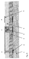
- FIG. 1 shows a schematic cross section through fully integrated printable electronics as are required, for example, for a complete transponder circuit.
- FIG. 2 once again shows all of the components which can also be seen in FIG. 1 but, in this case, the semiconductive layer at the location of the diode is not pulled as far as the level of the upper electrode of the other components but rather the upper electrode of the diode is deeper in this case.
- FIG. 3 shows a structure for supplying voltage; in this case, the components of a diode, a capacitor and a contact via are simultaneously produced on a substrate.
- FIG. 4 finally shows a composite body which combines an electrical contact via, a transistor and a resistor and/or a coil.
- the substrate 1 can be seen at the bottom of FIG. 1 . All insulating materials having a smooth surface can be used as the substrate; flexible and rigid materials alike can be used. Flexible films such as PET film or other polymer plastic films, glass, quartz, ceramic or another material are used, for example, at that location.
- the layer 2 which follows the substrate 1 is the first conductive layer or the lower electrode 2 which is applied in patterned form.
- the source and drain electrodes which are covered by the subsequent semiconductor layer are produced here.
- Only conductive materials can be used for the conductive layer 2 , in which case it is not important whether they are organic or inorganic materials or a composite material.
- a metal or an alloy having a work function in the range of 4.6-5.2 eV, preferably 4.9 eV is used as the material for the conductive layer which is in contact with the semiconductive layer.
- Silver having a work function of 4.9 eV is particularly preferably used at that location.
- the work function is matched to the Fermi level of the semiconductor in such a manner that the difference to the Fermi level of the semiconductor is preferably 0.3 eV or less. It is then ensured that the charge carriers pass from the semiconductive material into the conductive material without any problems.
- the semiconductive layer 3 which, on account of its viscosity, is applied in unpatterned form under certain circumstances follows the first and lower electrode layer.
- Organic materials such as P3AT, P3DHTT, regioregular polyalkylthiophenes, polyfluorene derivatives, PPVs, in general, and/or other polymers, for example with a conjugated main chain or a freely mobile electron pair in the main chain, are preferably used as materials for the semiconductive layer.
- the semiconductive layer 3 may also be applied in patterned form, for example by means of printing.
- an insulating layer 4 which has to be applied in patterned form only insofar as a dielectric layer or insulating layer should be omitted at that/those location(s) on the substrate at which diodes or contact vias are produced because it would interfere.
- the insulating layer 4 is composed, for example, of a soluble printable material.
- Organic soluble materials for example polystyrene derivatives, PMMA or generally insulating polymers, are preferably used as materials for the insulating layer.
- the patterned insulating layer 4 is followed by an upper conductive layer 5 which in turn is preferably patterned.
- Conductive organic and inorganic materials and/or composite materials are used in this case.
- Metals whose work function is different to that of the material of the lower conductive layer (counterelectrode) are preferably used, in particular.
- materials whose work function is in the range of from 3 to 5 eV, in particular from 3.0 eV to 4.6 eV, or above, are used in this case; copper, nickel, chromium, cobalt, manganese etc. are successfully used in this case, for example.
- an electrical contact via a is a transistor b whose source/drain electrodes are in the lower conductive layer 2 .
- a diode c in which the semiconductive layer 3 is pulled up as far as the level of the counterelectrode 5 so that no current/voltage losses are produced is arranged beside the transistor b.
- a capacitor d can be seen to the right of the diode c and a resistor or a coil e is in turn situated to the right of said capacitor, that is to say on the far right on the outside.
- FIG. 3 all of the essential components needed to supply voltage to a rectifier are implemented together on a substrate and, if all of the layers are common in all of the components, can be simultaneously produced.
- the layer sequence corresponds to that from FIG. 1 , the same materials or other corresponding materials also being able to be used.
- the layer 1 is thus the substrate, the layer 2 , patterned, is a conductive layer, 3 is the semiconductor layer, 4 is the insulating layer and 5 is the counterelectrode which is in turn patterned.
- the following sequence of components is provided: on the far left on the outside is the contact via 1 , the diode c is next to the latter and the capacitor d follows the diode c.
- An alternating voltage coming from an antenna can be rectified, for example, using the composite body shown here.
- the semiconductor is applied in a somewhat thicker form in the diode region c; this may be achieved, for example, via a using a decorative print during simultaneous production of the components.
- FIG. 4 shows a multilayer composite body which combines an electrical contact via, a transistor and a resistor or a coil.
- At least PFETs Polymer Field Effect Transistor
- inverters Inverters
- ring oscillators flip-flops
- frequency dividers and/or counters can be constructed using this layer structure and this arrangement of the components of the electrical contact via a, transistor b and resistor or coil e.
- the layer structure again corresponds to that known from the other figures. Although a diode is not implemented in this case, the conductive material of the upper electrode 5 and of the lower electrode 2 may be entirely different, particularly in terms of its work function.
- encapsulation and/or sealing of the components which may comprise a wide variety of materials and/or laminates, is still recommended as the uppermost layer or termination.
- the encapsulation/sealing may be composed of a rigid or flexible material.
- the essential parts of electronic devices such as a transistor, field effect transistor, electrical contact via, resistor, interconnect resistor, inductance, diode, capacitor and rectifier are implemented, can be produced next to one another and/or behind one another on a substrate using this structure by means of layers which are continuously applied in a planar manner and/or patterned layers.
- the cost-effective production which is suitable for mass production, of preferably all components in the subassembly at the same time and in a continuous method makes it possible for individual components to contain layers which, in particular, have no function there; for example, in a field effect transistor and/or in a capacitor, the gate electrode may have a work function that differs from that of the source/drain electrode, the difference in the work function having no functionality in this case.
- the capacitor and the interconnect resistors and likewise the contact via contain, for example, a semiconductor which is superfluous at that location and is not functional.
- the essential parts of complex electronic devices such as a field effect transistor, electrical contact via, resistor, interconnect resistor, coil, diode, capacitor and rectifier, can be produced next to one another and/or behind one another on a substrate using the structure shown in the figures by means of layers which are continuously applied in a planar manner and/or patterned layers.
- the invention provides, for the first time, a possibility for a structure of an entire subassembly such as an RFID tag, the entire tag with all of the components being able to be implemented in one production process. As a result, a cost-effective production method which is suitable for mass production is described for the first time.
Landscapes
- Engineering & Computer Science (AREA)
- Microelectronics & Electronic Packaging (AREA)
- Computer Hardware Design (AREA)
- Physics & Mathematics (AREA)
- General Physics & Mathematics (AREA)
- Theoretical Computer Science (AREA)
- Semiconductor Integrated Circuits (AREA)
- Thin Film Transistor (AREA)
- Fixed Capacitors And Capacitor Manufacturing Machines (AREA)
- Parts Printed On Printed Circuit Boards (AREA)
Applications Claiming Priority (4)
| Application Number | Priority Date | Filing Date | Title |
|---|---|---|---|
| DE102005017655.0 | 2005-04-15 | ||
| DE102005017655 | 2005-04-15 | ||
| DE102005017655A DE102005017655B4 (de) | 2005-04-15 | 2005-04-15 | Mehrschichtiger Verbundkörper mit elektronischer Funktion |
| PCT/EP2006/002916 WO2006108514A2 (fr) | 2005-04-15 | 2006-03-31 | Élément composite à plusieurs couches ayant une fonction électronique |
Publications (2)
| Publication Number | Publication Date |
|---|---|
| US20080203383A1 US20080203383A1 (en) | 2008-08-28 |
| US7812343B2 true US7812343B2 (en) | 2010-10-12 |
Family
ID=37084894
Family Applications (1)
| Application Number | Title | Priority Date | Filing Date |
|---|---|---|---|
| US11/911,429 Expired - Fee Related US7812343B2 (en) | 2005-04-15 | 2006-03-31 | Multilayer composite body having an electronic function |
Country Status (8)
| Country | Link |
|---|---|
| US (1) | US7812343B2 (fr) |
| EP (1) | EP1869625A2 (fr) |
| JP (1) | JP4977126B2 (fr) |
| KR (1) | KR101244124B1 (fr) |
| CN (1) | CN101160594B (fr) |
| DE (1) | DE102005017655B4 (fr) |
| TW (1) | TWI314369B (fr) |
| WO (1) | WO2006108514A2 (fr) |
Cited By (3)
| Publication number | Priority date | Publication date | Assignee | Title |
|---|---|---|---|---|
| US20100224959A1 (en) * | 2006-06-07 | 2010-09-09 | Nxp B.V. | Semiconductor Chip, Transponder and Method of Manufacturing a Transponder |
| US20100243742A1 (en) * | 2007-09-27 | 2010-09-30 | Andreas Ullmann | Rfid transponder |
| US7940340B2 (en) | 2005-07-04 | 2011-05-10 | Polyic Gmbh & Co. Kg | Multilayer body with electrically controllable optically active systems of layers |
Families Citing this family (3)
| Publication number | Priority date | Publication date | Assignee | Title |
|---|---|---|---|---|
| DE102008036736B4 (de) * | 2008-08-07 | 2010-04-29 | Abb Ag | Elektrisches Installationsschaltgerät mit einer elektronischen Baugruppe |
| DE102008061928A1 (de) * | 2008-12-15 | 2010-06-17 | Polylc Gmbh & Co. Kg | Organisch elektronische Schaltung |
| DE102013102052B4 (de) | 2013-03-01 | 2018-07-26 | Infineon Technologies Ag | Chip-Anordnung |
Citations (244)
| Publication number | Priority date | Publication date | Assignee | Title |
|---|---|---|---|---|
| GB723598A (en) | 1951-09-07 | 1955-02-09 | Philips Nv | Improvements in or relating to methods of producing electrically conductive mouldings from plastics |
| US3512052A (en) | 1968-01-11 | 1970-05-12 | Gen Motors Corp | Metal-insulator-semiconductor voltage variable capacitor with controlled resistivity dielectric |
| US3769096A (en) | 1971-03-12 | 1973-10-30 | Bell Telephone Labor Inc | Pyroelectric devices |
| AU488652B2 (en) | 1973-09-26 | 1976-04-01 | Commonwealth Scientific And Industrial Research Organisation | Improvements in or relating to security tokens |
| US3955098A (en) | 1973-10-12 | 1976-05-04 | Hitachi, Ltd. | Switching circuit having floating gate mis load transistors |
| US3999122A (en) | 1974-02-14 | 1976-12-21 | Siemens Aktiengesellschaft | Semiconductor sensing device for fluids |
| DE2102735B2 (de) | 1971-01-21 | 1979-05-10 | Transformatoren Union Ag, 7000 Stuttgart | Einrichtung zur Regelung des Mengendurchsatzes von Mühlen und Brechern |
| US4246298A (en) | 1979-03-14 | 1981-01-20 | American Can Company | Rapid curing of epoxy resin coating compositions by combination of photoinitiation and controlled heat application |
| US4302648A (en) | 1978-01-26 | 1981-11-24 | Shin-Etsu Polymer Co., Ltd. | Key-board switch unit |
| US4340057A (en) | 1980-12-24 | 1982-07-20 | S. C. Johnson & Son, Inc. | Radiation induced graft polymerization |
| GB2058462B (en) | 1979-09-10 | 1983-08-03 | Shinetsu Polymer Co | Push button switch |
| US4442019A (en) | 1978-05-26 | 1984-04-10 | Marks Alvin M | Electroordered dipole suspension |
| US4472627A (en) | 1982-09-30 | 1984-09-18 | The United States Of America As Represented By The Secretary Of The Treasury | Authenticating and anti-counterfeiting device for currency |
| DE3338597A1 (de) | 1983-10-24 | 1985-05-02 | GAO Gesellschaft für Automation und Organisation mbH, 8000 München | Datentraeger mit integriertem schaltkreis und verfahren zur herstellung desselben |
| US4554229A (en) | 1984-04-06 | 1985-11-19 | At&T Technologies, Inc. | Multilayer hybrid integrated circuit |
| EP0108650A3 (fr) | 1982-11-09 | 1986-02-12 | Zytrex Corporation | Transistor MOS programmable |
| JPS6265472A (ja) | 1985-09-18 | 1987-03-24 | Toshiba Corp | Mis型半導体素子 |
| EP0128529A3 (fr) | 1983-06-10 | 1987-07-29 | BASF Aktiengesellschaft | Interrupteur à pression |
| DE3705109A1 (de) | 1986-02-24 | 1987-08-27 | Rca Corp | Display |
| EP0268370A2 (fr) | 1986-10-13 | 1988-05-25 | Canon Kabushiki Kaisha | Commutateur |
| US4865197A (en) | 1988-03-04 | 1989-09-12 | Unisys Corporation | Electronic component transportation container |
| US4926052A (en) | 1986-03-03 | 1990-05-15 | Kabushiki Kaisha Toshiba | Radiation detecting device |
| US4937119A (en) | 1988-12-15 | 1990-06-26 | Hoechst Celanese Corp. | Textured organic optical data storage media and methods of preparation |
| EP0442123A1 (fr) | 1990-01-04 | 1991-08-21 | Neste Oy | Méthode de préparation de composants électroniques et électro-optiques et de circuits utilisant des polymères conducteurs |
| US5053679A (en) | 1989-03-21 | 1991-10-01 | Centre National D'etudes Des Telecommunications | Photoconductive-electroluminescent memory effect polychromatic display |
| US5075816A (en) | 1989-08-11 | 1991-12-24 | Vaisala Oy | Capacitive humidity sensor construction and method for manufacturing the sensor |
| EP0501456A2 (fr) | 1991-02-26 | 1992-09-02 | Sony Corporation | Ordinateur de jeux vidéo muni d'un lecteur de disques optiques |
| EP0511807A1 (fr) | 1991-04-27 | 1992-11-04 | Gec Avery Limited | Appareil et unité capteur pour afficher l'évolution d'une grandeur physique dans le temps |
| US5173835A (en) | 1991-10-15 | 1992-12-22 | Motorola, Inc. | Voltage variable capacitor |
| US5202677A (en) | 1991-01-31 | 1993-04-13 | Crystal Images, Inc. | Display apparatus using thermochromic material |
| US5206525A (en) | 1989-12-27 | 1993-04-27 | Nippon Petrochemicals Co., Ltd. | Electric element capable of controlling the electric conductivity of π-conjugated macromolecular materials |
| DE4103675C2 (de) | 1991-02-07 | 1993-10-21 | Telefunken Microelectron | Schaltung zur Spannungsüberhöhung von Wechselspannungs-Eingangssignalen |
| US5259926A (en) | 1991-09-24 | 1993-11-09 | Hitachi, Ltd. | Method of manufacturing a thin-film pattern on a substrate |
| EP0350179B1 (fr) | 1988-06-21 | 1994-01-19 | Gec Avery Limited | Fabrication des cartes électroniques portables |
| EP0588721A1 (fr) | 1992-09-18 | 1994-03-23 | Commissariat A L'energie Atomique | Support à réseau d'éléments résistifs en polymère conducteur et son procédé de fabrication |
| US5321240A (en) | 1992-01-30 | 1994-06-14 | Mitsubishi Denki Kabushiki Kaisha | Non-contact IC card |
| EP0603939A2 (fr) | 1992-12-21 | 1994-06-29 | Koninklijke Philips Electronics N.V. | Polymère conducteur de type N et méthode de préparation d'un tel polymère |
| DE4243832A1 (de) | 1992-12-23 | 1994-06-30 | Daimler Benz Ag | Tastsensoranordnung |
| US5347144A (en) | 1990-07-04 | 1994-09-13 | Centre National De La Recherche Scientifique (Cnrs) | Thin-layer field-effect transistors with MIS structure whose insulator and semiconductor are made of organic materials |
| US5364735A (en) | 1988-07-01 | 1994-11-15 | Sony Corporation | Multiple layer optical record medium with protective layers and method for producing same |
| US5395504A (en) | 1993-02-04 | 1995-03-07 | Asulab S.A. | Electrochemical measuring system with multizone sensors |
| EP0418504B1 (fr) | 1989-07-25 | 1995-04-05 | Matsushita Electric Industrial Co., Ltd. | Dispositif mémoire à semi-conducteur organique de structure MISFET et sa méthode de contrôle |
| EP0528662B1 (fr) | 1991-08-15 | 1995-11-02 | Kabushiki Kaisha Toshiba | Transistor à effet de champ organique |
| EP0685985A2 (fr) | 1994-05-31 | 1995-12-06 | Hitachi Metals, Ltd. | Haut-parleur piézoélectrique et procédé pour sa fabrication |
| US5480839A (en) | 1993-01-15 | 1996-01-02 | Kabushiki Kaisha Toshiba | Semiconductor device manufacturing method |
| US5486851A (en) | 1991-10-30 | 1996-01-23 | Fraunhofer-Gesellschaft Zur Forderung Der Angewandten Forschung E.V. | Illumination device using a pulsed laser source a Schlieren optical system and a matrix addressable surface light modulator for producing images with undifracted light |
| US5502396A (en) | 1993-09-21 | 1996-03-26 | Asulab S.A. | Measuring device with connection for a removable sensor |
| EP0716458A2 (fr) | 1994-12-09 | 1996-06-12 | AT&T Corp. | Méthode de fabrication d'un transistor organique à couche mince et article fait par cette méthode |
| US5528222A (en) | 1994-09-09 | 1996-06-18 | International Business Machines Corporation | Radio frequency circuit and memory in thin flexible package |
| US5546889A (en) | 1993-10-06 | 1996-08-20 | Matsushita Electric Industrial Co., Ltd. | Method of manufacturing organic oriented film and method of manufacturing electronic device |
| DE19506907A1 (de) | 1995-02-28 | 1996-09-05 | Telefunken Microelectron | Schaltungsanordnung zur Variation eines Eingangssignals mit bestimmter Eingangsspannung und bestimmtem Eingangsstrom |
| US5569879A (en) | 1991-02-19 | 1996-10-29 | Gemplus Card International | Integrated circuit micromodule obtained by the continuous assembly of patterned strips |
| US5578513A (en) | 1993-09-17 | 1996-11-26 | Mitsubishi Denki Kabushiki Kaisha | Method of making a semiconductor device having a gate all around type of thin film transistor |
| US5580794A (en) | 1993-08-24 | 1996-12-03 | Metrika Laboratories, Inc. | Disposable electronic assay device |
| DE19629291A1 (de) | 1995-07-21 | 1997-01-23 | Oki Electric Ind Co Ltd | Energieversorgungsschaltung für einen Transponder, die mit geringer Leistung betreibbar ist |
| DE4312766C2 (de) | 1993-04-20 | 1997-02-27 | Telefunken Microelectron | Schaltung zur Spannungsüberhöhung |
| US5625199A (en) | 1996-01-16 | 1997-04-29 | Lucent Technologies Inc. | Article comprising complementary circuit with inorganic n-channel and organic p-channel thin film transistors |
| US5625474A (en) | 1995-06-02 | 1997-04-29 | Sharp Kabushiki Kaisha | Full-color liquid crystal display device and fabrication process therefor |
| US5629530A (en) | 1994-05-16 | 1997-05-13 | U.S. Phillips Corporation | Semiconductor device having an organic semiconductor material |
| DE19648937A1 (de) | 1996-11-26 | 1997-05-15 | Meonic Sys Eng Gmbh | Elektronisches Etikett |
| US5630986A (en) | 1995-01-13 | 1997-05-20 | Bayer Corporation | Dispensing instrument for fluid monitoring sensors |
| US5652645A (en) | 1995-07-24 | 1997-07-29 | Anvik Corporation | High-throughput, high-resolution, projection patterning system for large, flexible, roll-fed, electronic-module substrates |
| DE19610284A1 (de) | 1996-03-15 | 1997-08-07 | Siemens Ag | Antennenspule |
| US5691089A (en) | 1993-03-25 | 1997-11-25 | Texas Instruments Incorporated | Integrated circuits formed in radiation sensitive material and method of forming same |
| US5693956A (en) | 1996-07-29 | 1997-12-02 | Motorola | Inverted oleds on hard plastic substrate |
| US5705826A (en) | 1994-06-28 | 1998-01-06 | Hitachi, Ltd. | Field-effect transistor having a semiconductor layer made of an organic compound |
| US5707894A (en) | 1995-10-27 | 1998-01-13 | United Microelectronics Corporation | Bonding pad structure and method thereof |
| US5729428A (en) | 1995-04-25 | 1998-03-17 | Nec Corporation | Solid electrolytic capacitor with conductive polymer as solid electrolyte and method for fabricating the same |
| EP0786820A3 (fr) | 1996-01-29 | 1998-07-01 | Motorola, Inc. | Transistor organique à film mince à mobilité de charge augmentée |
| EP0615256B1 (fr) | 1993-03-09 | 1998-09-23 | Koninklijke Philips Electronics N.V. | Méthode de fabrication d'une configuration d'un polymère électroconducteur à la surface d'un substrat et procédé de métallisation de cette configuration |
| US5869972A (en) | 1996-02-26 | 1999-02-09 | Birch; Brian Jeffrey | Testing device using a thermochromic display and method of using same |
| US5883397A (en) | 1993-07-01 | 1999-03-16 | Mitsubishi Denki Kabushiki Kaisha | Plastic functional element |
| US5892244A (en) | 1989-01-10 | 1999-04-06 | Mitsubishi Denki Kabushiki Kaisha | Field effect transistor including πconjugate polymer and liquid crystal display including the field effect transistor |
| DE19852312A1 (de) | 1997-11-12 | 1999-05-20 | Nintendo Co Ltd | Tragbare Informationsverarbeitungseinheit |
| US5946551A (en) | 1997-03-25 | 1999-08-31 | Dimitrakopoulos; Christos Dimitrios | Fabrication of thin film effect transistor comprising an organic semiconductor and chemical solution deposited metal oxide gate dielectric |
| US5967048A (en) | 1998-06-12 | 1999-10-19 | Howard A. Fromson | Method and apparatus for the multiple imaging of a continuous web |
| US5970318A (en) | 1997-05-15 | 1999-10-19 | Electronics And Telecommunications Research Institute | Fabrication method of an organic electroluminescent devices |
| US5973598A (en) | 1997-09-11 | 1999-10-26 | Precision Dynamics Corporation | Radio frequency identification tag on flexible substrate |
| JP2969184B2 (ja) | 1990-04-09 | 1999-11-02 | カシオ計算機株式会社 | 薄膜トランジスタメモリ |
| DE19816860A1 (de) | 1998-03-06 | 1999-11-18 | Deutsche Telekom Ag | Chipkarte, insbesondere Guthabenkarte |
| DE19918193A1 (de) | 1998-04-24 | 1999-11-25 | Cambridge Display Tech Ltd | Selektives Aufbringen von Polymerfilmen |
| US5994773A (en) | 1996-03-06 | 1999-11-30 | Hirakawa; Tadashi | Ball grid array semiconductor package |
| US5998805A (en) | 1997-12-11 | 1999-12-07 | Motorola, Inc. | Active matrix OED array with improved OED cathode |
| US5997817A (en) | 1997-12-05 | 1999-12-07 | Roche Diagnostics Corporation | Electrochemical biosensor test strip |
| EP0962984A2 (fr) | 1998-05-29 | 1999-12-08 | Lucent Technologies Inc. | Transistor à couche mince intégré monolithique avec une diode organique émettrice de lumière |
| EP0690457B1 (fr) | 1994-05-23 | 1999-12-22 | Al-Coat Ltd. | Solution à base de polyaniline, articles revêtus de polyaniline et procédés pour sa préparation |
| EP0981165A1 (fr) | 1998-08-20 | 2000-02-23 | Lucent Technologies Inc. | Transistors en couche mince |
| US6036919A (en) | 1996-07-23 | 2000-03-14 | Roche Diagnostic Gmbh | Diagnostic test carrier with multilayer field |
| EP0989614A2 (fr) | 1998-09-04 | 2000-03-29 | Sel Semiconductor Energy Laboratory Co., Ltd. | TFT avec une structure LDD et sa méthode de fabrication |
| US6045977A (en) | 1998-02-19 | 2000-04-04 | Lucent Technologies Inc. | Process for patterning conductive polyaniline films |
| DE19851703A1 (de) | 1998-10-30 | 2000-05-04 | Inst Halbleiterphysik Gmbh | Verfahren zur Herstellung von elektronischen Strukturen |
| US6072716A (en) | 1999-04-14 | 2000-06-06 | Massachusetts Institute Of Technology | Memory structures and methods of making same |
| JP2000173770A (ja) | 1998-10-13 | 2000-06-23 | Sony Internatl Europ Gmbh | アクティブマトリクス方式表示装置及びその製造方法 |
| US6083104A (en) | 1998-01-16 | 2000-07-04 | Silverlit Toys (U.S.A.), Inc. | Programmable toy with an independent game cartridge |
| US6087196A (en) | 1998-01-30 | 2000-07-11 | The Trustees Of Princeton University | Fabrication of organic semiconductor devices using ink jet printing |
| US6107920A (en) | 1998-06-09 | 2000-08-22 | Motorola, Inc. | Radio frequency identification tag having an article integrated antenna |
| US6133835A (en) | 1997-12-05 | 2000-10-17 | U.S. Philips Corporation | Identification transponder |
| EP1052594A1 (fr) | 1999-05-14 | 2000-11-15 | Sokymat S.A. | Transpondeur et moule ainsi que leur procédé de fabrication |
| EP1065725A2 (fr) | 1999-06-28 | 2001-01-03 | Sel Semiconductor Energy Laboratory Co., Ltd. | Méthode de fabrication d'un dispositif électro-optique |
| DE19933757A1 (de) | 1999-07-19 | 2001-01-25 | Giesecke & Devrient Gmbh | Chipkarte mit integrierter Batterie |
| US6180956B1 (en) | 1999-03-03 | 2001-01-30 | International Business Machine Corp. | Thin film transistors with organic-inorganic hybrid materials as semiconducting channels |
| DE19935527A1 (de) | 1999-07-28 | 2001-02-08 | Giesecke & Devrient Gmbh | Aktive Folie für Chipkarten mit Display |
| DE19937262A1 (de) | 1999-08-06 | 2001-03-01 | Siemens Ag | Anordnung mit Transistor-Funktion |
| US6197663B1 (en) | 1999-12-07 | 2001-03-06 | Lucent Technologies Inc. | Process for fabricating integrated circuit devices having thin film transistors |
| DE19921024C2 (de) | 1999-05-06 | 2001-03-08 | Wolfgang Eichelmann | Videospielanlage |
| US6207472B1 (en) | 1999-03-09 | 2001-03-27 | International Business Machines Corporation | Low temperature thin film transistor fabrication |
| JP2001085272A (ja) | 1999-07-14 | 2001-03-30 | Matsushita Electric Ind Co Ltd | 可変容量コンデンサ |
| US6221553B1 (en) | 1999-01-15 | 2001-04-24 | 3M Innovative Properties Company | Thermal transfer element for forming multilayer devices |
| EP1102335A2 (fr) | 1999-11-17 | 2001-05-23 | Lucent Technologies Inc. | Transistor à couche mince |
| JP2001147659A (ja) | 1999-11-18 | 2001-05-29 | Sony Corp | 表示装置 |
| EP1104035A2 (fr) | 1999-11-29 | 2001-05-30 | Lucent Technologies Inc. | Transistor à couche mince |
| EP1103916A1 (fr) | 1999-11-24 | 2001-05-30 | Infineon Technologies AG | Carte à puce |
| FR2793089B3 (fr) | 1999-04-28 | 2001-06-08 | Rene Liger | Transpondeur a antenne integree |
| US6251513B1 (en) | 1997-11-08 | 2001-06-26 | Littlefuse, Inc. | Polymer composites for overvoltage protection |
| WO2001047044A2 (fr) | 1999-12-21 | 2001-06-28 | Plastic Logic Limited | Formation d'interconnexions |
| US20010006846A1 (en) | 1999-04-26 | 2001-07-05 | Min Cao | Method and structure for bonding layers in a semiconductor device |
| US6259506B1 (en) | 1997-02-18 | 2001-07-10 | Spectra Science Corporation | Field activated security articles including polymer dispersed liquid crystals, and including micro-encapsulated field affected materials |
| DE69519782T2 (de) | 1994-10-03 | 2001-08-02 | News Datacom Ltd., London | System mit gesichertem Zugang |
| US6291126B2 (en) | 1999-01-15 | 2001-09-18 | 3M Innovative Properties Company | Thermal transfer element and process for forming organic electroluminescent devices |
| EP1134694A1 (fr) | 2000-03-16 | 2001-09-19 | Infineon Technologies AG | Document avec circuit électronique intégré |
| DE10012204A1 (de) | 2000-03-13 | 2001-09-20 | Siemens Ag | Einrichtung zum Kennzeichnen von Stückgut |
| JP2001267578A (ja) | 2000-03-17 | 2001-09-28 | Sony Corp | 薄膜半導体装置及びその製造方法 |
| US20010026187A1 (en) | 2000-03-07 | 2001-10-04 | Satoru Oku | Booster, IC card having the same, and electronic equipment having the same |
| WO2001073109A2 (fr) | 2000-03-28 | 2001-10-04 | Diabetes Diagnostics, Inc. | Procede de fabrication en continu de capteur electrochimque jetable |
| US6300141B1 (en) | 1999-03-02 | 2001-10-09 | Helix Biopharma Corporation | Card-based biosensor device |
| US6322736B1 (en) | 1998-03-27 | 2001-11-27 | Agere Systems Inc. | Method for fabricating molded microstructures on substrates |
| US6321571B1 (en) | 1998-12-21 | 2001-11-27 | Corning Incorporated | Method of making glass structures for flat panel displays |
| US20010046081A1 (en) | 2000-01-31 | 2001-11-29 | Naoyuki Hayashi | Sheet-like display, sphere-like resin body, and micro-capsule |
| US6326288B1 (en) | 1999-07-06 | 2001-12-04 | Elmos Semiconductor Ag | CMOS compatible SOI process |
| US20010048341A1 (en) | 2000-05-29 | 2001-12-06 | Stmicroelectronics Ltd. | Programmable glitch filter |
| US6329226B1 (en) | 2000-06-01 | 2001-12-11 | Agere Systems Guardian Corp. | Method for fabricating a thin-film transistor |
| US6330464B1 (en) | 1998-08-26 | 2001-12-11 | Sensors For Medicine & Science | Optical-based sensing devices |
| US6335539B1 (en) | 1999-11-05 | 2002-01-01 | International Business Machines Corporation | Method for improving performance of organic semiconductors in bottom electrode structure |
| DE20111825U1 (de) | 2001-07-20 | 2002-01-17 | Lammering, Thomas, Dipl.-Ing., 33335 Gütersloh | Printmedium |
| US6340822B1 (en) | 1999-10-05 | 2002-01-22 | Agere Systems Guardian Corp. | Article comprising vertically nano-interconnected circuit devices and method for making the same |
| US6344662B1 (en) | 1997-03-25 | 2002-02-05 | International Business Machines Corporation | Thin-film field-effect transistor with organic-inorganic hybrid semiconductor requiring low operating voltages |
| US20020018911A1 (en) | 1999-05-11 | 2002-02-14 | Mark T. Bernius | Electroluminescent or photocell device having protective packaging |
| US20020022284A1 (en) | 1991-02-27 | 2002-02-21 | Alan J. Heeger | Visible light emitting diodes fabricated from soluble semiconducting polymers |
| US6350996B1 (en) * | 1998-04-24 | 2002-02-26 | Canon Kabushiki Kaisha | Light emitting diode device |
| US20020025391A1 (en) | 1989-05-26 | 2002-02-28 | Marie Angelopoulos | Patterns of electrically conducting polymers and their application as electrodes or electrical contacts |
| US6362509B1 (en) | 1999-10-11 | 2002-03-26 | U.S. Philips Electronics | Field effect transistor with organic semiconductor layer |
| US6366017B1 (en) | 1999-07-14 | 2002-04-02 | Agilent Technologies, Inc/ | Organic light emitting diodes with distributed bragg reflector |
| DE10045192A1 (de) | 2000-09-13 | 2002-04-04 | Siemens Ag | Organischer Datenspeicher, RFID-Tag mit organischem Datenspeicher, Verwendung eines organischen Datenspeichers |
| DE10043204A1 (de) | 2000-09-01 | 2002-04-04 | Siemens Ag | Organischer Feld-Effekt-Transistor, Verfahren zur Strukturierung eines OFETs und integrierte Schaltung |
| US6369793B1 (en) | 1998-03-30 | 2002-04-09 | David C. Zimman | Printed display and battery |
| DE10047171A1 (de) | 2000-09-22 | 2002-04-18 | Siemens Ag | Elektrode und/oder Leiterbahn für organische Bauelemente und Herstellungverfahren dazu |
| US6384804B1 (en) | 1998-11-25 | 2002-05-07 | Lucent Techonologies Inc. | Display comprising organic smart pixels |
| US20020053320A1 (en) | 1998-12-15 | 2002-05-09 | Gregg M. Duthaler | Method for printing of transistor arrays on plastic substrates |
| US20020056839A1 (en) | 2000-11-11 | 2002-05-16 | Pt Plus Co. Ltd. | Method of crystallizing a silicon thin film and semiconductor device fabricated thereby |
| DE10058559A1 (de) | 2000-11-24 | 2002-05-29 | Interactiva Biotechnologie Gmb | System zur Abwicklung eines Warentransfers und Warenvorrats-Behälter |
| US20020068392A1 (en) | 2000-12-01 | 2002-06-06 | Pt Plus Co. Ltd. | Method for fabricating thin film transistor including crystalline silicon active layer |
| US6403396B1 (en) | 1998-01-28 | 2002-06-11 | Thin Film Electronics Asa | Method for generation of electrically conducting or semiconducting structures in three dimensions and methods for erasure of the same structures |
| US6414728B1 (en) | 1994-04-21 | 2002-07-02 | Reveo, Inc. | Image display system having direct and projection viewing modes |
| US6429450B1 (en) | 1997-08-22 | 2002-08-06 | Koninklijke Philips Electronics N.V. | Method of manufacturing a field-effect transistor substantially consisting of organic materials |
| WO2002065557A1 (fr) | 2001-02-09 | 2002-08-22 | Siemens Aktiengesellschaft | Transistor a effet de champ organique a dielectrique de grille photostructure, son procede de production et son utilisation en electronique organique |
| US20020130042A1 (en) | 2000-03-02 | 2002-09-19 | Moerman Piet H.C. | Combined lancet and electrochemical analyte-testing apparatus |
| EP0964516B1 (fr) | 1997-05-12 | 2002-10-16 | Agilent Technologies, Inc. (a Delaware corporation) | Oscillateur en anneau entrelacé, commandé par tension,entièrement intégré à grande vitesse |
| EP1251720A2 (fr) | 2001-03-26 | 2002-10-23 | Pioneer Corporation | Dispositif à diode électroluminescente organique et affichage organique électroluminescent |
| DE10120687A1 (de) | 2001-04-27 | 2002-10-31 | Siemens Ag | Verkapseltes organisch-elektronisches Bauteil, Verfahren zu seiner Herstellung und seine Verwendung |
| DE10120686A1 (de) | 2001-04-27 | 2002-11-07 | Siemens Ag | Verfahren zur Erzeugung dünner homogener Schichten mit Hilfe der Siebdrucktechnik, Vorrichtung zur Durchführung des Verfahren und ihre Verwendung |
| WO2002091495A2 (fr) | 2001-05-07 | 2002-11-14 | Coatue Corporation | Memoire moleculaire |
| DE10033112C2 (de) | 2000-07-07 | 2002-11-14 | Siemens Ag | Verfahren zur Herstellung und Strukturierung organischer Feldeffekt-Transistoren (OFET), hiernach gefertigter OFET und seine Verwendung |
| US6483473B1 (en) | 2000-07-18 | 2002-11-19 | Marconi Communications Inc. | Wireless communication device and method |
| US20020170897A1 (en) | 2001-05-21 | 2002-11-21 | Hall Frank L. | Methods for preparing ball grid array substrates via use of a laser |
| WO2002095805A2 (fr) | 2001-05-23 | 2002-11-28 | Plastic Logic Limited | Formation de motif sur des dispositifs |
| DE10126859A1 (de) | 2001-06-01 | 2002-12-12 | Siemens Ag | Verfahren zur Erzeugung von leitfähigen Strukturen mittels Drucktechnik sowie daraus hergestellte aktive Bauelemente für integrierte Schaltungen |
| US6498114B1 (en) | 1999-04-09 | 2002-12-24 | E Ink Corporation | Method for forming a patterned semiconductor film |
| US20020195644A1 (en) | 2001-06-08 | 2002-12-26 | Ananth Dodabalapur | Organic polarizable gate transistor apparatus and method |
| EP0435029B2 (fr) | 1989-12-22 | 2003-01-02 | GAO Gesellschaft für Automation und Organisation mbH | Support d'information avec élément de sécurité à cristaux liquides |
| EP0979715B1 (fr) | 1998-08-10 | 2003-01-15 | Adolf Illig Maschinenbau GmbH & Co. KG | Dispositif de chauffage pour chauffer des plaques en matière thermoplastique et procédé pour ajuster la température de ce dispositif de chauffage |
| DE10151440C1 (de) | 2001-10-18 | 2003-02-06 | Siemens Ag | Organisches Elektronikbauteil, Verfahren zu seiner Herstellung und seine Verwendung |
| US6517955B1 (en) | 1999-02-22 | 2003-02-11 | Nippon Steel Corporation | High strength galvanized steel plate excellent in adhesion of plated metal and formability in press working and high strength alloy galvanized steel plate and method for production thereof |
| US6518949B2 (en) | 1998-04-10 | 2003-02-11 | E Ink Corporation | Electronic displays using organic-based field effect transistors |
| US6521109B1 (en) | 1999-09-13 | 2003-02-18 | Interuniversitair Microelektronica Centrum (Imec) Vzw | Device for detecting an analyte in a sample based on organic materials |
| US6528816B1 (en) | 1998-06-19 | 2003-03-04 | Thomas Jackson | Integrated inorganic/organic complementary thin-film transistor circuit and a method for its production |
| DE10141440A1 (de) | 2001-08-23 | 2003-03-13 | Daimler Chrysler Ag | Tripodegelenk |
| EP1296280A1 (fr) | 1997-09-11 | 2003-03-26 | Precision Dynamics Corporation | Etiquette d'identification RF comportant une puce consistant de matériaux organiques |
| US20030059987A1 (en) | 1999-12-21 | 2003-03-27 | Plastic Logic Limited | Inkjet-fabricated integrated circuits |
| US6541130B2 (en) | 1999-05-12 | 2003-04-01 | Pioneer Corporation | Organic electroluminescence multi-color display and method of fabricating the same |
| US6548875B2 (en) | 2000-03-06 | 2003-04-15 | Kabushiki Kaisha Toshiba | Sub-tenth micron misfet with source and drain layers formed over source and drains, sloping away from the gate |
| US20030070500A1 (en) | 2001-10-15 | 2003-04-17 | Yu-Nan Hung | Drive gear shaft structure of a self-moving type |
| US6555840B1 (en) | 1999-02-16 | 2003-04-29 | Sharp Kabushiki Kaisha | Charge-transport structures |
| US6566156B1 (en) | 1996-06-12 | 2003-05-20 | The Trustees Of Princeton University | Patterning of thin films for the fabrication of organic multi-color displays |
| DE10153656A1 (de) | 2001-10-31 | 2003-05-22 | Infineon Technologies Ag | Verfahren zur Verringerung des Kontaktwiderstandes in organischen Feldeffekttransistoren durch Aufbringen einer reaktiven, die organische Halbleiterschicht im Kontaktbereich regio-selektiv dotierenden Zwischenschicht |
| DE10061297C2 (de) | 2000-12-08 | 2003-05-28 | Siemens Ag | Verfahren zur Sturkturierung eines OFETs |
| DE10126860C2 (de) | 2001-06-01 | 2003-05-28 | Siemens Ag | Organischer Feldeffekt-Transistor, Verfahren zu seiner Herstellung und Verwendung zum Aufbau integrierter Schaltungen |
| US20030112576A1 (en) | 2001-09-28 | 2003-06-19 | Brewer Peter D. | Process for producing high performance interconnects |
| DE10163267A1 (de) | 2001-12-21 | 2003-07-03 | Giesecke & Devrient Gmbh | Blattgut mit einem elektrischen Schaltkreis sowie Vorrichtung und Verfahren zur Bearbeitung des Blattguts |
| US6593690B1 (en) | 1999-09-03 | 2003-07-15 | 3M Innovative Properties Company | Large area organic electronic devices having conducting polymer buffer layers and methods of making same |
| US6596569B1 (en) | 2002-03-15 | 2003-07-22 | Lucent Technologies Inc. | Thin film transistors |
| US20030141807A1 (en) | 2001-01-31 | 2003-07-31 | Takeo Kawase | Display device |
| US6603139B1 (en) | 1998-04-16 | 2003-08-05 | Cambridge Display Technology Limited | Polymer devices |
| US6621098B1 (en) | 1999-11-29 | 2003-09-16 | The Penn State Research Foundation | Thin-film transistor and methods of manufacturing and incorporating a semiconducting organic material |
| US20030178620A1 (en) | 2000-09-11 | 2003-09-25 | Adolf Bernds | Organic rectifier, circuit, rfid tag and use of an organic rectifier |
| DE10209400A1 (de) | 2002-03-04 | 2003-10-02 | Infineon Technologies Ag | Transponderschaltung mit einer Gleichrichterschaltung sowie Verfahren zur Herstellung einer Transponderschaltung mit einer Gleichrichterschaltung |
| DE10219905A1 (de) | 2002-05-03 | 2003-12-04 | Osram Opto Semiconductors Gmbh | Optoelektronisches Bauelement und Verfahren zur Herstellung |
| US20030227664A1 (en) | 2000-05-24 | 2003-12-11 | Anoop Agrawal | Electrochromic devices |
| US20040002176A1 (en) | 2002-06-28 | 2004-01-01 | Xerox Corporation | Organic ferroelectric memory cells |
| EP1383179A2 (fr) | 2002-07-17 | 2004-01-21 | Pioneer Corporation | Dispositif semiconducteur organique |
| US20040013982A1 (en) | 1999-09-14 | 2004-01-22 | Massachusetts Institute Of Technology | Fabrication of finely featured devices by liquid embossing |
| DE10229168A1 (de) | 2002-06-28 | 2004-01-29 | Infineon Technologies Ag | Laminat mit einer als Antennenstruktur ausgebildeten elektrisch leitfähigen Schicht |
| US6686693B1 (en) | 1999-09-06 | 2004-02-03 | Futaba Denshi Kogyo Kabushiki Kaisha | Organic electroluminescent device with disjointed electrodes arranged in groups |
| DE10212640B4 (de) | 2002-03-21 | 2004-02-05 | Siemens Ag | Logische Bauteile aus organischen Feldeffekttransistoren |
| US20040029310A1 (en) | 2000-08-18 | 2004-02-12 | Adoft Bernds | Organic field-effect transistor (ofet), a production method therefor, an integrated circut constructed from the same and their uses |
| US20040026689A1 (en) | 2000-08-18 | 2004-02-12 | Adolf Bernds | Encapsulated organic-electronic component, method for producing the same and use thereof |
| US6699728B2 (en) | 2000-09-06 | 2004-03-02 | Osram Opto Semiconductors Gmbh | Patterning of electrodes in oled devices |
| EP1318084A4 (fr) | 2000-08-30 | 2004-03-31 | Nippon Oxygen Co Ltd | Conteneur isotherme |
| DE10341962A1 (de) | 2002-10-15 | 2004-04-29 | Atomic Austria Gmbh | Elektronisches Überwachungssystem für eine aus mehreren Sportartikeln bestehende Sportartikelkombination und deren Anwendung |
| US20040084670A1 (en) | 2002-11-04 | 2004-05-06 | Tripsas Nicholas H. | Stacked organic memory devices and methods of operating and fabricating |
| US20040092196A1 (en) | 2000-06-06 | 2004-05-13 | Peter Van De Witte | Liquid crystal display device |
| US6736985B1 (en) | 1999-05-05 | 2004-05-18 | Agere Systems Inc. | High-resolution method for patterning a substrate with micro-printing |
| WO2004042837A2 (fr) | 2002-11-05 | 2004-05-21 | Siemens Aktiengesellschaft | Composant electronique organique a structuration haute resolution et procede de production de ce composant |
| WO2004047194A2 (fr) | 2002-11-19 | 2004-06-03 | Polyic Gmbh & Co.Kg | Composant electronique organique comportant le meme materiau organique pour au moins deux couches fonctionnelles |
| WO2004047144A2 (fr) | 2002-11-19 | 2004-06-03 | Polyic Gmbh & Co.Kg | Composant electronique organique comportant une couche fonctionnelle semiconductrice structuree et procede de fabrication de ce composant |
| EP1048912B1 (fr) | 1999-04-29 | 2004-06-16 | Miele & Cie. KG | Appareil frigorifique et procédé d'indication des germes |
| US20040119504A1 (en) | 2002-12-23 | 2004-06-24 | 3M Innovative Properties Company | AC powered logic circuitry |
| US20040160389A1 (en) | 1996-01-17 | 2004-08-19 | Nippon Telegraph And Telephone Corporation | Optical device and three-dimensional display device |
| DE10117663B4 (de) | 2001-04-09 | 2004-09-02 | Samsung SDI Co., Ltd., Suwon | Verfahren zur Herstellung von Matrixanordnungen auf Basis verschiedenartiger organischer leitfähiger Materialien |
| DE69913745T2 (de) | 1999-05-17 | 2004-10-07 | Goodyear Tire & Rubber | Rf transponder und verfahren zur steuerung der rf signalmodulation in einem passiven transponder |
| US20040211329A1 (en) | 2001-09-18 | 2004-10-28 | Katsuyuki Funahata | Pattern forming method and pattern forming device |
| US20040233065A1 (en) | 2000-01-11 | 2004-11-25 | Freeman Jeffrey R. | Package location system |
| US20040239586A1 (en) | 2003-05-30 | 2004-12-02 | Eastman Kodak Company | Flexible display |
| DE10330064B3 (de) | 2003-07-03 | 2004-12-09 | Siemens Ag | Logikgatter mit potentialfreier Gate-Elektrode für organische integrierte Schaltungen |
| US20040246413A1 (en) | 2003-06-05 | 2004-12-09 | Eastman Kodak Company | UV curable conductive materials in displays |
| DE10330063A1 (de) | 2003-07-03 | 2005-02-03 | Siemens Ag | Verfahren zur Strukturierung und Integration organischer Schichten unter Schutz |
| US6859093B1 (en) | 2000-11-28 | 2005-02-22 | Precision Dynamics Corporation | Rectifying charge storage device with bi-stable states |
| DE10335336A1 (de) | 2003-08-01 | 2005-03-03 | Siemens Ag | Feldeffektbauelemente und Kondensatoren mit Elektrodenanordnung in einer Schichtebene |
| DE10338277A1 (de) | 2003-08-20 | 2005-03-17 | Siemens Ag | Organischer Kondensator mit spannungsgesteuerter Kapazität |
| EP1215725A3 (fr) | 2000-12-18 | 2005-03-23 | cubit electronics Gmbh | Assemblage utilisé pour supporter des dispositifs électriques et transpondeur sans contacts |
| US20050062066A1 (en) | 2003-09-24 | 2005-03-24 | Lucent Technologies, Inc. | Semiconductor devices having regions of induced high and low conductivity, and methods of making the same |
| DE10340641A1 (de) | 2003-09-03 | 2005-04-07 | Siemens Ag | Strukturierung von Gate-Dielektrika in organischen Feldeffekt-Transistoren |
| US20050098775A1 (en) | 2003-09-11 | 2005-05-12 | Seiko Epson Corporation | Method of forming wirings for tile-shaped elements, structures of wirings for tile-shaped elements, and electronic equipment |
| US20050127357A1 (en) | 2003-12-12 | 2005-06-16 | Palo Alto Research Center, Inc. | Thin-film transistor array with ring geometry |
| US20050168340A1 (en) | 2002-03-18 | 2005-08-04 | Mosher Walter W.Jr. | Enhanced identification appliance having a plurality or data sets for authentication |
| EP1083775A4 (fr) | 1999-03-29 | 2005-12-07 | Seiko Epson Corp | Composition, procede de preparation d'un film, et element fonctionnel et son procede de preparation |
| US6999297B1 (en) * | 1999-01-20 | 2006-02-14 | U.S. Philips Corporation | Breakdown-resistant thin film capacitor with interdigitated structure |
| EP0966182B1 (fr) | 1998-06-17 | 2006-04-26 | Lg Electronics Inc. | Procédé pour la fabrication d'un panneau d'affichage |
| US7064345B2 (en) | 2001-12-11 | 2006-06-20 | Siemens Aktiengesellschaft | Organic field effect transistor with off-set threshold voltage and the use thereof |
| EP1237207A3 (fr) | 2001-03-02 | 2006-06-21 | Fuji Photo Film Co., Ltd. | Méthode de production d'un dispositif organique à couche mince et matériau de transfert utilisé dans ce procédé |
| EP1224999A4 (fr) | 1999-09-28 | 2007-05-02 | Sumitomo Heavy Industries | Procede et dispositif de per age par laser |
| EP1401245A4 (fr) | 2001-06-27 | 2007-07-11 | Sony Corp | Element electroluminescent |
| EP1113502B1 (fr) | 1999-03-30 | 2007-09-19 | Seiko Epson Corporation | Procede de fabrication d'un transistor a couches minces |
| EP1434281A3 (fr) | 2002-12-26 | 2007-10-24 | Konica Minolta Holdings, Inc. | Méthode de fabrication d'un transistor à couche mince, substrat et circuit électrique |
| EP1170851B1 (fr) | 2000-07-03 | 2010-02-24 | Texas Instruments Deutschland Gmbh | Assemblage de circuit pour doubler la tension d'une batterie |
Family Cites Families (9)
| Publication number | Priority date | Publication date | Assignee | Title |
|---|---|---|---|---|
| US65757A (en) * | 1867-06-11 | Improved lifter foe the lids of pitchers | ||
| JP3466954B2 (ja) * | 1998-04-24 | 2003-11-17 | キヤノン株式会社 | 発光ダイオード装置及びその製造方法 |
| WO2001008242A1 (fr) * | 1999-07-21 | 2001-02-01 | E Ink Corporation | Procedes preferes de production d'elements de circuits electriques utilises pour commander un affichage electronique |
| AU781584B2 (en) * | 1999-12-21 | 2005-06-02 | Flexenable Limited | Solution processed devices |
| US6414543B1 (en) * | 2000-11-28 | 2002-07-02 | Precision Dynamics Corporation | Rectifying charge storage element |
| KR100388272B1 (ko) * | 2000-12-26 | 2003-06-19 | 삼성에스디아이 주식회사 | 티알에스 소자 |
| KR20030024690A (ko) * | 2001-04-17 | 2003-03-26 | 코닌클리케 필립스 일렉트로닉스 엔.브이. | 저 황산염 및 고 금속 이온 함량을 갖는 전도성 투명중합체 층을 포함하는 led |
| US6819181B2 (en) * | 2001-12-21 | 2004-11-16 | Motorola, Inc. | Method and structure for integrated circuit interference isolation enhancement |
| WO2004063806A1 (fr) * | 2003-01-09 | 2004-07-29 | Polyic Gmbh & Co. Kg | Platine ou substrat pour un appareil electronique organique et utilisation de ladite platine |
-
2005
- 2005-04-15 DE DE102005017655A patent/DE102005017655B4/de not_active Expired - Fee Related
-
2006
- 2006-03-31 WO PCT/EP2006/002916 patent/WO2006108514A2/fr not_active Ceased
- 2006-03-31 CN CN200680012163.5A patent/CN101160594B/zh not_active Expired - Fee Related
- 2006-03-31 EP EP06723879A patent/EP1869625A2/fr not_active Withdrawn
- 2006-03-31 KR KR1020077023640A patent/KR101244124B1/ko not_active Expired - Fee Related
- 2006-03-31 JP JP2008505763A patent/JP4977126B2/ja not_active Expired - Fee Related
- 2006-03-31 US US11/911,429 patent/US7812343B2/en not_active Expired - Fee Related
- 2006-04-04 TW TW095111903A patent/TWI314369B/zh not_active IP Right Cessation
Patent Citations (277)
| Publication number | Priority date | Publication date | Assignee | Title |
|---|---|---|---|---|
| GB723598A (en) | 1951-09-07 | 1955-02-09 | Philips Nv | Improvements in or relating to methods of producing electrically conductive mouldings from plastics |
| US3512052A (en) | 1968-01-11 | 1970-05-12 | Gen Motors Corp | Metal-insulator-semiconductor voltage variable capacitor with controlled resistivity dielectric |
| DE2102735B2 (de) | 1971-01-21 | 1979-05-10 | Transformatoren Union Ag, 7000 Stuttgart | Einrichtung zur Regelung des Mengendurchsatzes von Mühlen und Brechern |
| US3769096A (en) | 1971-03-12 | 1973-10-30 | Bell Telephone Labor Inc | Pyroelectric devices |
| AU488652B2 (en) | 1973-09-26 | 1976-04-01 | Commonwealth Scientific And Industrial Research Organisation | Improvements in or relating to security tokens |
| US3955098A (en) | 1973-10-12 | 1976-05-04 | Hitachi, Ltd. | Switching circuit having floating gate mis load transistors |
| US3999122A (en) | 1974-02-14 | 1976-12-21 | Siemens Aktiengesellschaft | Semiconductor sensing device for fluids |
| US4302648A (en) | 1978-01-26 | 1981-11-24 | Shin-Etsu Polymer Co., Ltd. | Key-board switch unit |
| US4442019A (en) | 1978-05-26 | 1984-04-10 | Marks Alvin M | Electroordered dipole suspension |
| US4246298A (en) | 1979-03-14 | 1981-01-20 | American Can Company | Rapid curing of epoxy resin coating compositions by combination of photoinitiation and controlled heat application |
| GB2058462B (en) | 1979-09-10 | 1983-08-03 | Shinetsu Polymer Co | Push button switch |
| US4340057A (en) | 1980-12-24 | 1982-07-20 | S. C. Johnson & Son, Inc. | Radiation induced graft polymerization |
| US4472627A (en) | 1982-09-30 | 1984-09-18 | The United States Of America As Represented By The Secretary Of The Treasury | Authenticating and anti-counterfeiting device for currency |
| EP0108650A3 (fr) | 1982-11-09 | 1986-02-12 | Zytrex Corporation | Transistor MOS programmable |
| EP0128529A3 (fr) | 1983-06-10 | 1987-07-29 | BASF Aktiengesellschaft | Interrupteur à pression |
| DE3338597A1 (de) | 1983-10-24 | 1985-05-02 | GAO Gesellschaft für Automation und Organisation mbH, 8000 München | Datentraeger mit integriertem schaltkreis und verfahren zur herstellung desselben |
| US4554229A (en) | 1984-04-06 | 1985-11-19 | At&T Technologies, Inc. | Multilayer hybrid integrated circuit |
| JPS6265472A (ja) | 1985-09-18 | 1987-03-24 | Toshiba Corp | Mis型半導体素子 |
| DE3705109A1 (de) | 1986-02-24 | 1987-08-27 | Rca Corp | Display |
| US4926052A (en) | 1986-03-03 | 1990-05-15 | Kabushiki Kaisha Toshiba | Radiation detecting device |
| EP0268370A3 (en) | 1986-10-13 | 1989-05-31 | Canon Kabushiki Kaisha | Switching device |
| EP0268370A2 (fr) | 1986-10-13 | 1988-05-25 | Canon Kabushiki Kaisha | Commutateur |
| US4865197A (en) | 1988-03-04 | 1989-09-12 | Unisys Corporation | Electronic component transportation container |
| EP0350179B1 (fr) | 1988-06-21 | 1994-01-19 | Gec Avery Limited | Fabrication des cartes électroniques portables |
| US5364735A (en) | 1988-07-01 | 1994-11-15 | Sony Corporation | Multiple layer optical record medium with protective layers and method for producing same |
| US4937119A (en) | 1988-12-15 | 1990-06-26 | Hoechst Celanese Corp. | Textured organic optical data storage media and methods of preparation |
| US6060338A (en) | 1989-01-10 | 2000-05-09 | Mitsubishi Denki Kabushiki Kaisha | Method of making a field effect transistor |
| US5892244A (en) | 1989-01-10 | 1999-04-06 | Mitsubishi Denki Kabushiki Kaisha | Field effect transistor including πconjugate polymer and liquid crystal display including the field effect transistor |
| US5053679A (en) | 1989-03-21 | 1991-10-01 | Centre National D'etudes Des Telecommunications | Photoconductive-electroluminescent memory effect polychromatic display |
| US20020025391A1 (en) | 1989-05-26 | 2002-02-28 | Marie Angelopoulos | Patterns of electrically conducting polymers and their application as electrodes or electrical contacts |
| EP0418504B1 (fr) | 1989-07-25 | 1995-04-05 | Matsushita Electric Industrial Co., Ltd. | Dispositif mémoire à semi-conducteur organique de structure MISFET et sa méthode de contrôle |
| US5075816A (en) | 1989-08-11 | 1991-12-24 | Vaisala Oy | Capacitive humidity sensor construction and method for manufacturing the sensor |
| EP0435029B2 (fr) | 1989-12-22 | 2003-01-02 | GAO Gesellschaft für Automation und Organisation mbH | Support d'information avec élément de sécurité à cristaux liquides |
| US5206525A (en) | 1989-12-27 | 1993-04-27 | Nippon Petrochemicals Co., Ltd. | Electric element capable of controlling the electric conductivity of π-conjugated macromolecular materials |
| EP0460242B1 (fr) | 1989-12-27 | 1996-04-17 | Nippon Petrochemicals Co., Ltd. | Element electrique et procede de reglage de la conductivite |
| EP0442123A1 (fr) | 1990-01-04 | 1991-08-21 | Neste Oy | Méthode de préparation de composants électroniques et électro-optiques et de circuits utilisant des polymères conducteurs |
| JP2969184B2 (ja) | 1990-04-09 | 1999-11-02 | カシオ計算機株式会社 | 薄膜トランジスタメモリ |
| US5347144A (en) | 1990-07-04 | 1994-09-13 | Centre National De La Recherche Scientifique (Cnrs) | Thin-layer field-effect transistors with MIS structure whose insulator and semiconductor are made of organic materials |
| US5202677A (en) | 1991-01-31 | 1993-04-13 | Crystal Images, Inc. | Display apparatus using thermochromic material |
| DE4103675C2 (de) | 1991-02-07 | 1993-10-21 | Telefunken Microelectron | Schaltung zur Spannungsüberhöhung von Wechselspannungs-Eingangssignalen |
| US5569879A (en) | 1991-02-19 | 1996-10-29 | Gemplus Card International | Integrated circuit micromodule obtained by the continuous assembly of patterned strips |
| EP0501456A2 (fr) | 1991-02-26 | 1992-09-02 | Sony Corporation | Ordinateur de jeux vidéo muni d'un lecteur de disques optiques |
| EP0501456A3 (fr) | 1991-02-26 | 1992-09-09 | Sony Corporation | Ordinateur de jeux vidéo muni d'un lecteur de disques optiques |
| US20020022284A1 (en) | 1991-02-27 | 2002-02-21 | Alan J. Heeger | Visible light emitting diodes fabricated from soluble semiconducting polymers |
| EP0511807A1 (fr) | 1991-04-27 | 1992-11-04 | Gec Avery Limited | Appareil et unité capteur pour afficher l'évolution d'une grandeur physique dans le temps |
| EP0528662B1 (fr) | 1991-08-15 | 1995-11-02 | Kabushiki Kaisha Toshiba | Transistor à effet de champ organique |
| US5259926A (en) | 1991-09-24 | 1993-11-09 | Hitachi, Ltd. | Method of manufacturing a thin-film pattern on a substrate |
| DE69232740T2 (de) | 1991-10-15 | 2002-12-05 | Motorola, Inc. | Spannungsvariabler kondensator |
| US5173835A (en) | 1991-10-15 | 1992-12-22 | Motorola, Inc. | Voltage variable capacitor |
| US5486851A (en) | 1991-10-30 | 1996-01-23 | Fraunhofer-Gesellschaft Zur Forderung Der Angewandten Forschung E.V. | Illumination device using a pulsed laser source a Schlieren optical system and a matrix addressable surface light modulator for producing images with undifracted light |
| US5321240A (en) | 1992-01-30 | 1994-06-14 | Mitsubishi Denki Kabushiki Kaisha | Non-contact IC card |
| EP0588721A1 (fr) | 1992-09-18 | 1994-03-23 | Commissariat A L'energie Atomique | Support à réseau d'éléments résistifs en polymère conducteur et son procédé de fabrication |
| EP0603939A2 (fr) | 1992-12-21 | 1994-06-29 | Koninklijke Philips Electronics N.V. | Polymère conducteur de type N et méthode de préparation d'un tel polymère |
| DE4243832A1 (de) | 1992-12-23 | 1994-06-30 | Daimler Benz Ag | Tastsensoranordnung |
| US5480839A (en) | 1993-01-15 | 1996-01-02 | Kabushiki Kaisha Toshiba | Semiconductor device manufacturing method |
| US5395504A (en) | 1993-02-04 | 1995-03-07 | Asulab S.A. | Electrochemical measuring system with multizone sensors |
| EP0615256B1 (fr) | 1993-03-09 | 1998-09-23 | Koninklijke Philips Electronics N.V. | Méthode de fabrication d'une configuration d'un polymère électroconducteur à la surface d'un substrat et procédé de métallisation de cette configuration |
| US5691089A (en) | 1993-03-25 | 1997-11-25 | Texas Instruments Incorporated | Integrated circuits formed in radiation sensitive material and method of forming same |
| DE4312766C2 (de) | 1993-04-20 | 1997-02-27 | Telefunken Microelectron | Schaltung zur Spannungsüberhöhung |
| US5883397A (en) | 1993-07-01 | 1999-03-16 | Mitsubishi Denki Kabushiki Kaisha | Plastic functional element |
| US5580794A (en) | 1993-08-24 | 1996-12-03 | Metrika Laboratories, Inc. | Disposable electronic assay device |
| US5578513A (en) | 1993-09-17 | 1996-11-26 | Mitsubishi Denki Kabushiki Kaisha | Method of making a semiconductor device having a gate all around type of thin film transistor |
| US5502396A (en) | 1993-09-21 | 1996-03-26 | Asulab S.A. | Measuring device with connection for a removable sensor |
| US5546889A (en) | 1993-10-06 | 1996-08-20 | Matsushita Electric Industrial Co., Ltd. | Method of manufacturing organic oriented film and method of manufacturing electronic device |
| US6414728B1 (en) | 1994-04-21 | 2002-07-02 | Reveo, Inc. | Image display system having direct and projection viewing modes |
| US5629530A (en) | 1994-05-16 | 1997-05-13 | U.S. Phillips Corporation | Semiconductor device having an organic semiconductor material |
| EP0690457B1 (fr) | 1994-05-23 | 1999-12-22 | Al-Coat Ltd. | Solution à base de polyaniline, articles revêtus de polyaniline et procédés pour sa préparation |
| EP0685985A2 (fr) | 1994-05-31 | 1995-12-06 | Hitachi Metals, Ltd. | Haut-parleur piézoélectrique et procédé pour sa fabrication |
| US5854139A (en) | 1994-06-28 | 1998-12-29 | Hitachi, Ltd. | Organic field-effect transistor and production thereof |
| US5705826A (en) | 1994-06-28 | 1998-01-06 | Hitachi, Ltd. | Field-effect transistor having a semiconductor layer made of an organic compound |
| US5528222A (en) | 1994-09-09 | 1996-06-18 | International Business Machines Corporation | Radio frequency circuit and memory in thin flexible package |
| DE69519782T2 (de) | 1994-10-03 | 2001-08-02 | News Datacom Ltd., London | System mit gesichertem Zugang |
| EP0716458A3 (fr) | 1994-12-09 | 1997-11-26 | AT&T Corp. | Méthode de fabrication d'un transistor organique à couche mince et article fait par cette méthode |
| EP0716458A2 (fr) | 1994-12-09 | 1996-06-12 | AT&T Corp. | Méthode de fabrication d'un transistor organique à couche mince et article fait par cette méthode |
| US5574291A (en) | 1994-12-09 | 1996-11-12 | Lucent Technologies Inc. | Article comprising a thin film transistor with low conductivity organic layer |
| US5630986A (en) | 1995-01-13 | 1997-05-20 | Bayer Corporation | Dispensing instrument for fluid monitoring sensors |
| DE19506907A1 (de) | 1995-02-28 | 1996-09-05 | Telefunken Microelectron | Schaltungsanordnung zur Variation eines Eingangssignals mit bestimmter Eingangsspannung und bestimmtem Eingangsstrom |
| US5729428A (en) | 1995-04-25 | 1998-03-17 | Nec Corporation | Solid electrolytic capacitor with conductive polymer as solid electrolyte and method for fabricating the same |
| US5625474A (en) | 1995-06-02 | 1997-04-29 | Sharp Kabushiki Kaisha | Full-color liquid crystal display device and fabrication process therefor |
| DE19629291A1 (de) | 1995-07-21 | 1997-01-23 | Oki Electric Ind Co Ltd | Energieversorgungsschaltung für einen Transponder, die mit geringer Leistung betreibbar ist |
| US5652645A (en) | 1995-07-24 | 1997-07-29 | Anvik Corporation | High-throughput, high-resolution, projection patterning system for large, flexible, roll-fed, electronic-module substrates |
| US5707894A (en) | 1995-10-27 | 1998-01-13 | United Microelectronics Corporation | Bonding pad structure and method thereof |
| US5625199A (en) | 1996-01-16 | 1997-04-29 | Lucent Technologies Inc. | Article comprising complementary circuit with inorganic n-channel and organic p-channel thin film transistors |
| EP0785578A2 (fr) | 1996-01-16 | 1997-07-23 | AT&T Corp. | Circuit comportant des transistors à couche mince complémentaires |
| EP0785578A3 (fr) | 1996-01-16 | 1998-04-22 | AT&T Corp. | Circuit comportant des transistors à couche mince complémentaires |
| US20040160389A1 (en) | 1996-01-17 | 2004-08-19 | Nippon Telegraph And Telephone Corporation | Optical device and three-dimensional display device |
| EP0786820A3 (fr) | 1996-01-29 | 1998-07-01 | Motorola, Inc. | Transistor organique à film mince à mobilité de charge augmentée |
| US5869972A (en) | 1996-02-26 | 1999-02-09 | Birch; Brian Jeffrey | Testing device using a thermochromic display and method of using same |
| US5994773A (en) | 1996-03-06 | 1999-11-30 | Hirakawa; Tadashi | Ball grid array semiconductor package |
| DE19610284A1 (de) | 1996-03-15 | 1997-08-07 | Siemens Ag | Antennenspule |
| US6566156B1 (en) | 1996-06-12 | 2003-05-20 | The Trustees Of Princeton University | Patterning of thin films for the fabrication of organic multi-color displays |
| US6036919A (en) | 1996-07-23 | 2000-03-14 | Roche Diagnostic Gmbh | Diagnostic test carrier with multilayer field |
| US5693956A (en) | 1996-07-29 | 1997-12-02 | Motorola | Inverted oleds on hard plastic substrate |
| DE19648937A1 (de) | 1996-11-26 | 1997-05-15 | Meonic Sys Eng Gmbh | Elektronisches Etikett |
| US6259506B1 (en) | 1997-02-18 | 2001-07-10 | Spectra Science Corporation | Field activated security articles including polymer dispersed liquid crystals, and including micro-encapsulated field affected materials |
| US6344662B1 (en) | 1997-03-25 | 2002-02-05 | International Business Machines Corporation | Thin-film field-effect transistor with organic-inorganic hybrid semiconductor requiring low operating voltages |
| US5946551A (en) | 1997-03-25 | 1999-08-31 | Dimitrakopoulos; Christos Dimitrios | Fabrication of thin film effect transistor comprising an organic semiconductor and chemical solution deposited metal oxide gate dielectric |
| EP0964516B1 (fr) | 1997-05-12 | 2002-10-16 | Agilent Technologies, Inc. (a Delaware corporation) | Oscillateur en anneau entrelacé, commandé par tension,entièrement intégré à grande vitesse |
| US5970318A (en) | 1997-05-15 | 1999-10-19 | Electronics And Telecommunications Research Institute | Fabrication method of an organic electroluminescent devices |
| US6429450B1 (en) | 1997-08-22 | 2002-08-06 | Koninklijke Philips Electronics N.V. | Method of manufacturing a field-effect transistor substantially consisting of organic materials |
| US5973598A (en) | 1997-09-11 | 1999-10-26 | Precision Dynamics Corporation | Radio frequency identification tag on flexible substrate |
| EP1296280A1 (fr) | 1997-09-11 | 2003-03-26 | Precision Dynamics Corporation | Etiquette d'identification RF comportant une puce consistant de matériaux organiques |
| US6251513B1 (en) | 1997-11-08 | 2001-06-26 | Littlefuse, Inc. | Polymer composites for overvoltage protection |
| DE19852312A1 (de) | 1997-11-12 | 1999-05-20 | Nintendo Co Ltd | Tragbare Informationsverarbeitungseinheit |
| US5997817A (en) | 1997-12-05 | 1999-12-07 | Roche Diagnostics Corporation | Electrochemical biosensor test strip |
| US6133835A (en) | 1997-12-05 | 2000-10-17 | U.S. Philips Corporation | Identification transponder |
| US5998805A (en) | 1997-12-11 | 1999-12-07 | Motorola, Inc. | Active matrix OED array with improved OED cathode |
| US6083104A (en) | 1998-01-16 | 2000-07-04 | Silverlit Toys (U.S.A.), Inc. | Programmable toy with an independent game cartridge |
| US6403396B1 (en) | 1998-01-28 | 2002-06-11 | Thin Film Electronics Asa | Method for generation of electrically conducting or semiconducting structures in three dimensions and methods for erasure of the same structures |
| US6087196A (en) | 1998-01-30 | 2000-07-11 | The Trustees Of Princeton University | Fabrication of organic semiconductor devices using ink jet printing |
| US6045977A (en) | 1998-02-19 | 2000-04-04 | Lucent Technologies Inc. | Process for patterning conductive polyaniline films |
| DE19816860A1 (de) | 1998-03-06 | 1999-11-18 | Deutsche Telekom Ag | Chipkarte, insbesondere Guthabenkarte |
| US6322736B1 (en) | 1998-03-27 | 2001-11-27 | Agere Systems Inc. | Method for fabricating molded microstructures on substrates |
| US6369793B1 (en) | 1998-03-30 | 2002-04-09 | David C. Zimman | Printed display and battery |
| US6518949B2 (en) | 1998-04-10 | 2003-02-11 | E Ink Corporation | Electronic displays using organic-based field effect transistors |
| US6603139B1 (en) | 1998-04-16 | 2003-08-05 | Cambridge Display Technology Limited | Polymer devices |
| US6350996B1 (en) * | 1998-04-24 | 2002-02-26 | Canon Kabushiki Kaisha | Light emitting diode device |
| DE19918193A1 (de) | 1998-04-24 | 1999-11-25 | Cambridge Display Tech Ltd | Selektives Aufbringen von Polymerfilmen |
| JP2000029403A (ja) | 1998-05-29 | 2000-01-28 | Lucent Technol Inc | 有機発光ダイオ―ドとモノリシックに集積化された薄膜トランジスタ |
| EP0962984A2 (fr) | 1998-05-29 | 1999-12-08 | Lucent Technologies Inc. | Transistor à couche mince intégré monolithique avec une diode organique émettrice de lumière |
| US6150668A (en) | 1998-05-29 | 2000-11-21 | Lucent Technologies Inc. | Thin-film transistor monolithically integrated with an organic light-emitting diode |
| EP0962984A3 (fr) | 1998-05-29 | 2000-01-12 | Lucent Technologies Inc. | Transistor à couche mince intégré monolithique avec une diode organique émettrice de lumière |
| US6107920A (en) | 1998-06-09 | 2000-08-22 | Motorola, Inc. | Radio frequency identification tag having an article integrated antenna |
| US5967048A (en) | 1998-06-12 | 1999-10-19 | Howard A. Fromson | Method and apparatus for the multiple imaging of a continuous web |
| EP0966182B1 (fr) | 1998-06-17 | 2006-04-26 | Lg Electronics Inc. | Procédé pour la fabrication d'un panneau d'affichage |
| US6528816B1 (en) | 1998-06-19 | 2003-03-04 | Thomas Jackson | Integrated inorganic/organic complementary thin-film transistor circuit and a method for its production |
| EP0979715B1 (fr) | 1998-08-10 | 2003-01-15 | Adolf Illig Maschinenbau GmbH & Co. KG | Dispositif de chauffage pour chauffer des plaques en matière thermoplastique et procédé pour ajuster la température de ce dispositif de chauffage |
| EP0981165A1 (fr) | 1998-08-20 | 2000-02-23 | Lucent Technologies Inc. | Transistors en couche mince |
| US6215130B1 (en) | 1998-08-20 | 2001-04-10 | Lucent Technologies Inc. | Thin film transistors |
| US6330464B1 (en) | 1998-08-26 | 2001-12-11 | Sensors For Medicine & Science | Optical-based sensing devices |
| EP0989614A2 (fr) | 1998-09-04 | 2000-03-29 | Sel Semiconductor Energy Laboratory Co., Ltd. | TFT avec une structure LDD et sa méthode de fabrication |
| JP2000173770A (ja) | 1998-10-13 | 2000-06-23 | Sony Internatl Europ Gmbh | アクティブマトリクス方式表示装置及びその製造方法 |
| DE19851703A1 (de) | 1998-10-30 | 2000-05-04 | Inst Halbleiterphysik Gmbh | Verfahren zur Herstellung von elektronischen Strukturen |
| US6384804B1 (en) | 1998-11-25 | 2002-05-07 | Lucent Techonologies Inc. | Display comprising organic smart pixels |
| US20020053320A1 (en) | 1998-12-15 | 2002-05-09 | Gregg M. Duthaler | Method for printing of transistor arrays on plastic substrates |
| US6321571B1 (en) | 1998-12-21 | 2001-11-27 | Corning Incorporated | Method of making glass structures for flat panel displays |
| US6291126B2 (en) | 1999-01-15 | 2001-09-18 | 3M Innovative Properties Company | Thermal transfer element and process for forming organic electroluminescent devices |
| US6221553B1 (en) | 1999-01-15 | 2001-04-24 | 3M Innovative Properties Company | Thermal transfer element for forming multilayer devices |
| US6999297B1 (en) * | 1999-01-20 | 2006-02-14 | U.S. Philips Corporation | Breakdown-resistant thin film capacitor with interdigitated structure |
| US6555840B1 (en) | 1999-02-16 | 2003-04-29 | Sharp Kabushiki Kaisha | Charge-transport structures |
| US6517955B1 (en) | 1999-02-22 | 2003-02-11 | Nippon Steel Corporation | High strength galvanized steel plate excellent in adhesion of plated metal and formability in press working and high strength alloy galvanized steel plate and method for production thereof |
| US6300141B1 (en) | 1999-03-02 | 2001-10-09 | Helix Biopharma Corporation | Card-based biosensor device |
| US6180956B1 (en) | 1999-03-03 | 2001-01-30 | International Business Machine Corp. | Thin film transistors with organic-inorganic hybrid materials as semiconducting channels |
| DE10006257B8 (de) | 1999-03-03 | 2006-12-14 | International Business Machines Corporation | Dünnfilmtransistoren mit organisch-anorganischen Hybridmaterialien als halbleitende Kanäle |
| US6207472B1 (en) | 1999-03-09 | 2001-03-27 | International Business Machines Corporation | Low temperature thin film transistor fabrication |
| EP1083775A4 (fr) | 1999-03-29 | 2005-12-07 | Seiko Epson Corp | Composition, procede de preparation d'un film, et element fonctionnel et son procede de preparation |
| EP1113502B1 (fr) | 1999-03-30 | 2007-09-19 | Seiko Epson Corporation | Procede de fabrication d'un transistor a couches minces |
| US6498114B1 (en) | 1999-04-09 | 2002-12-24 | E Ink Corporation | Method for forming a patterned semiconductor film |
| US6072716A (en) | 1999-04-14 | 2000-06-06 | Massachusetts Institute Of Technology | Memory structures and methods of making same |
| US20010006846A1 (en) | 1999-04-26 | 2001-07-05 | Min Cao | Method and structure for bonding layers in a semiconductor device |
| FR2793089B3 (fr) | 1999-04-28 | 2001-06-08 | Rene Liger | Transpondeur a antenne integree |
| EP1048912B1 (fr) | 1999-04-29 | 2004-06-16 | Miele & Cie. KG | Appareil frigorifique et procédé d'indication des germes |
| US6736985B1 (en) | 1999-05-05 | 2004-05-18 | Agere Systems Inc. | High-resolution method for patterning a substrate with micro-printing |
| DE19921024C2 (de) | 1999-05-06 | 2001-03-08 | Wolfgang Eichelmann | Videospielanlage |
| US20020018911A1 (en) | 1999-05-11 | 2002-02-14 | Mark T. Bernius | Electroluminescent or photocell device having protective packaging |
| US6541130B2 (en) | 1999-05-12 | 2003-04-01 | Pioneer Corporation | Organic electroluminescence multi-color display and method of fabricating the same |
| EP1052594A1 (fr) | 1999-05-14 | 2000-11-15 | Sokymat S.A. | Transpondeur et moule ainsi que leur procédé de fabrication |
| DE69913745T2 (de) | 1999-05-17 | 2004-10-07 | Goodyear Tire & Rubber | Rf transponder und verfahren zur steuerung der rf signalmodulation in einem passiven transponder |
| EP1065725A2 (fr) | 1999-06-28 | 2001-01-03 | Sel Semiconductor Energy Laboratory Co., Ltd. | Méthode de fabrication d'un dispositif électro-optique |
| EP1065725A3 (fr) | 1999-06-28 | 2004-05-19 | Sel Semiconductor Energy Laboratory Co., Ltd. | Méthode de fabrication d'un dispositif électro-optique |
| US6326288B1 (en) | 1999-07-06 | 2001-12-04 | Elmos Semiconductor Ag | CMOS compatible SOI process |
| US6366017B1 (en) | 1999-07-14 | 2002-04-02 | Agilent Technologies, Inc/ | Organic light emitting diodes with distributed bragg reflector |
| JP2001085272A (ja) | 1999-07-14 | 2001-03-30 | Matsushita Electric Ind Co Ltd | 可変容量コンデンサ |
| DE19933757A1 (de) | 1999-07-19 | 2001-01-25 | Giesecke & Devrient Gmbh | Chipkarte mit integrierter Batterie |
| DE19935527A1 (de) | 1999-07-28 | 2001-02-08 | Giesecke & Devrient Gmbh | Aktive Folie für Chipkarten mit Display |
| DE19937262A1 (de) | 1999-08-06 | 2001-03-01 | Siemens Ag | Anordnung mit Transistor-Funktion |
| US6593690B1 (en) | 1999-09-03 | 2003-07-15 | 3M Innovative Properties Company | Large area organic electronic devices having conducting polymer buffer layers and methods of making same |
| US6686693B1 (en) | 1999-09-06 | 2004-02-03 | Futaba Denshi Kogyo Kabushiki Kaisha | Organic electroluminescent device with disjointed electrodes arranged in groups |
| US6521109B1 (en) | 1999-09-13 | 2003-02-18 | Interuniversitair Microelektronica Centrum (Imec) Vzw | Device for detecting an analyte in a sample based on organic materials |
| US20040013982A1 (en) | 1999-09-14 | 2004-01-22 | Massachusetts Institute Of Technology | Fabrication of finely featured devices by liquid embossing |
| EP1224999A4 (fr) | 1999-09-28 | 2007-05-02 | Sumitomo Heavy Industries | Procede et dispositif de per age par laser |
| US6340822B1 (en) | 1999-10-05 | 2002-01-22 | Agere Systems Guardian Corp. | Article comprising vertically nano-interconnected circuit devices and method for making the same |
| US6362509B1 (en) | 1999-10-11 | 2002-03-26 | U.S. Philips Electronics | Field effect transistor with organic semiconductor layer |
| US6335539B1 (en) | 1999-11-05 | 2002-01-01 | International Business Machines Corporation | Method for improving performance of organic semiconductors in bottom electrode structure |
| EP1102335A2 (fr) | 1999-11-17 | 2001-05-23 | Lucent Technologies Inc. | Transistor à couche mince |
| US6284562B1 (en) | 1999-11-17 | 2001-09-04 | Agere Systems Guardian Corp. | Thin film transistors |
| JP2001147659A (ja) | 1999-11-18 | 2001-05-29 | Sony Corp | 表示装置 |
| EP1103916A1 (fr) | 1999-11-24 | 2001-05-30 | Infineon Technologies AG | Carte à puce |
| US6621098B1 (en) | 1999-11-29 | 2003-09-16 | The Penn State Research Foundation | Thin-film transistor and methods of manufacturing and incorporating a semiconducting organic material |
| EP1104035A2 (fr) | 1999-11-29 | 2001-05-30 | Lucent Technologies Inc. | Transistor à couche mince |
| US6197663B1 (en) | 1999-12-07 | 2001-03-06 | Lucent Technologies Inc. | Process for fabricating integrated circuit devices having thin film transistors |
| WO2001047044A2 (fr) | 1999-12-21 | 2001-06-28 | Plastic Logic Limited | Formation d'interconnexions |
| WO2001047044A3 (fr) | 1999-12-21 | 2001-12-06 | Plastic Logic Ltd | Formation d'interconnexions |
| US20030059987A1 (en) | 1999-12-21 | 2003-03-27 | Plastic Logic Limited | Inkjet-fabricated integrated circuits |
| US20040233065A1 (en) | 2000-01-11 | 2004-11-25 | Freeman Jeffrey R. | Package location system |
| US20010046081A1 (en) | 2000-01-31 | 2001-11-29 | Naoyuki Hayashi | Sheet-like display, sphere-like resin body, and micro-capsule |
| US20020130042A1 (en) | 2000-03-02 | 2002-09-19 | Moerman Piet H.C. | Combined lancet and electrochemical analyte-testing apparatus |
| US6548875B2 (en) | 2000-03-06 | 2003-04-15 | Kabushiki Kaisha Toshiba | Sub-tenth micron misfet with source and drain layers formed over source and drains, sloping away from the gate |
| US20010026187A1 (en) | 2000-03-07 | 2001-10-04 | Satoru Oku | Booster, IC card having the same, and electronic equipment having the same |
| DE10012204A1 (de) | 2000-03-13 | 2001-09-20 | Siemens Ag | Einrichtung zum Kennzeichnen von Stückgut |
| EP1134694A1 (fr) | 2000-03-16 | 2001-09-19 | Infineon Technologies AG | Document avec circuit électronique intégré |
| JP2001267578A (ja) | 2000-03-17 | 2001-09-28 | Sony Corp | 薄膜半導体装置及びその製造方法 |
| WO2001073109A3 (fr) | 2000-03-28 | 2003-02-20 | Diabetes Diagnostics Inc | Procede de fabrication en continu de capteur electrochimque jetable |
| WO2001073109A2 (fr) | 2000-03-28 | 2001-10-04 | Diabetes Diagnostics, Inc. | Procede de fabrication en continu de capteur electrochimque jetable |
| US20030227664A1 (en) | 2000-05-24 | 2003-12-11 | Anoop Agrawal | Electrochromic devices |
| US20010048341A1 (en) | 2000-05-29 | 2001-12-06 | Stmicroelectronics Ltd. | Programmable glitch filter |
| US6329226B1 (en) | 2000-06-01 | 2001-12-11 | Agere Systems Guardian Corp. | Method for fabricating a thin-film transistor |
| US20040092196A1 (en) | 2000-06-06 | 2004-05-13 | Peter Van De Witte | Liquid crystal display device |
| EP1170851B1 (fr) | 2000-07-03 | 2010-02-24 | Texas Instruments Deutschland Gmbh | Assemblage de circuit pour doubler la tension d'une batterie |
| US6852583B2 (en) | 2000-07-07 | 2005-02-08 | Siemens Aktiengesellschaft | Method for the production and configuration of organic field-effect transistors (OFET) |
| DE10033112C2 (de) | 2000-07-07 | 2002-11-14 | Siemens Ag | Verfahren zur Herstellung und Strukturierung organischer Feldeffekt-Transistoren (OFET), hiernach gefertigter OFET und seine Verwendung |
| US6483473B1 (en) | 2000-07-18 | 2002-11-19 | Marconi Communications Inc. | Wireless communication device and method |
| US20040026689A1 (en) | 2000-08-18 | 2004-02-12 | Adolf Bernds | Encapsulated organic-electronic component, method for producing the same and use thereof |
| US20040029310A1 (en) | 2000-08-18 | 2004-02-12 | Adoft Bernds | Organic field-effect transistor (ofet), a production method therefor, an integrated circut constructed from the same and their uses |
| EP1318084A4 (fr) | 2000-08-30 | 2004-03-31 | Nippon Oxygen Co Ltd | Conteneur isotherme |
| DE10043204A1 (de) | 2000-09-01 | 2002-04-04 | Siemens Ag | Organischer Feld-Effekt-Transistor, Verfahren zur Strukturierung eines OFETs und integrierte Schaltung |
| US6960489B2 (en) | 2000-09-01 | 2005-11-01 | Siemens Aktiengesellschaft | Method for structuring an OFET |
| US6699728B2 (en) | 2000-09-06 | 2004-03-02 | Osram Opto Semiconductors Gmbh | Patterning of electrodes in oled devices |
| US20030178620A1 (en) | 2000-09-11 | 2003-09-25 | Adolf Bernds | Organic rectifier, circuit, rfid tag and use of an organic rectifier |
| US6903958B2 (en) | 2000-09-13 | 2005-06-07 | Siemens Aktiengesellschaft | Method of writing to an organic memory |
| DE10045192A1 (de) | 2000-09-13 | 2002-04-04 | Siemens Ag | Organischer Datenspeicher, RFID-Tag mit organischem Datenspeicher, Verwendung eines organischen Datenspeichers |
| DE10047171A1 (de) | 2000-09-22 | 2002-04-18 | Siemens Ag | Elektrode und/oder Leiterbahn für organische Bauelemente und Herstellungverfahren dazu |
| US20020056839A1 (en) | 2000-11-11 | 2002-05-16 | Pt Plus Co. Ltd. | Method of crystallizing a silicon thin film and semiconductor device fabricated thereby |
| DE10058559A1 (de) | 2000-11-24 | 2002-05-29 | Interactiva Biotechnologie Gmb | System zur Abwicklung eines Warentransfers und Warenvorrats-Behälter |
| US6859093B1 (en) | 2000-11-28 | 2005-02-22 | Precision Dynamics Corporation | Rectifying charge storage device with bi-stable states |
| US20020068392A1 (en) | 2000-12-01 | 2002-06-06 | Pt Plus Co. Ltd. | Method for fabricating thin film transistor including crystalline silicon active layer |
| US7229868B2 (en) | 2000-12-08 | 2007-06-12 | Polyic Gmbh & Co. Kg | Organic field-effect transistor, method for structuring an OFET and integrated circuit |
| US20040063267A1 (en) | 2000-12-08 | 2004-04-01 | Adolf Bernds | Organic field-effect transistor, method for structuring and ofet and integrated circuit |
| DE10061297C2 (de) | 2000-12-08 | 2003-05-28 | Siemens Ag | Verfahren zur Sturkturierung eines OFETs |
| EP1215725A3 (fr) | 2000-12-18 | 2005-03-23 | cubit electronics Gmbh | Assemblage utilisé pour supporter des dispositifs électriques et transpondeur sans contacts |
| US20030141807A1 (en) | 2001-01-31 | 2003-07-31 | Takeo Kawase | Display device |
| US7238961B2 (en) | 2001-02-09 | 2007-07-03 | Polyic Gmbh & Co. Kg | Organic field effect transistor with a photostructured gate dielectric, method for the production and use thereof in organic electronics |
| WO2002065557A1 (fr) | 2001-02-09 | 2002-08-22 | Siemens Aktiengesellschaft | Transistor a effet de champ organique a dielectrique de grille photostructure, son procede de production et son utilisation en electronique organique |
| EP1237207A3 (fr) | 2001-03-02 | 2006-06-21 | Fuji Photo Film Co., Ltd. | Méthode de production d'un dispositif organique à couche mince et matériau de transfert utilisé dans ce procédé |
| EP1251720A3 (fr) | 2001-03-26 | 2004-04-14 | Pioneer Corporation | Dispositif à diode électroluminescente organique et affichage organique électroluminescent |
| EP1251720A2 (fr) | 2001-03-26 | 2002-10-23 | Pioneer Corporation | Dispositif à diode électroluminescente organique et affichage organique électroluminescent |
| DE10117663B4 (de) | 2001-04-09 | 2004-09-02 | Samsung SDI Co., Ltd., Suwon | Verfahren zur Herstellung von Matrixanordnungen auf Basis verschiedenartiger organischer leitfähiger Materialien |
| DE10120686A1 (de) | 2001-04-27 | 2002-11-07 | Siemens Ag | Verfahren zur Erzeugung dünner homogener Schichten mit Hilfe der Siebdrucktechnik, Vorrichtung zur Durchführung des Verfahren und ihre Verwendung |
| DE10120687A1 (de) | 2001-04-27 | 2002-10-31 | Siemens Ag | Verkapseltes organisch-elektronisches Bauteil, Verfahren zu seiner Herstellung und seine Verwendung |
| WO2002091495A2 (fr) | 2001-05-07 | 2002-11-14 | Coatue Corporation | Memoire moleculaire |
| WO2002091495A3 (fr) | 2001-05-07 | 2003-08-21 | Coatue Corp | Memoire moleculaire |
| US20020170897A1 (en) | 2001-05-21 | 2002-11-21 | Hall Frank L. | Methods for preparing ball grid array substrates via use of a laser |
| WO2002095805A3 (fr) | 2001-05-23 | 2003-01-23 | Plastic Logic Ltd | Formation de motif sur des dispositifs |
| WO2002095805A2 (fr) | 2001-05-23 | 2002-11-28 | Plastic Logic Limited | Formation de motif sur des dispositifs |
| DE10126859A1 (de) | 2001-06-01 | 2002-12-12 | Siemens Ag | Verfahren zur Erzeugung von leitfähigen Strukturen mittels Drucktechnik sowie daraus hergestellte aktive Bauelemente für integrierte Schaltungen |
| DE10126860C2 (de) | 2001-06-01 | 2003-05-28 | Siemens Ag | Organischer Feldeffekt-Transistor, Verfahren zu seiner Herstellung und Verwendung zum Aufbau integrierter Schaltungen |
| US20020195644A1 (en) | 2001-06-08 | 2002-12-26 | Ananth Dodabalapur | Organic polarizable gate transistor apparatus and method |
| EP1401245A4 (fr) | 2001-06-27 | 2007-07-11 | Sony Corp | Element electroluminescent |
| DE20111825U1 (de) | 2001-07-20 | 2002-01-17 | Lammering, Thomas, Dipl.-Ing., 33335 Gütersloh | Printmedium |
| DE10141440A1 (de) | 2001-08-23 | 2003-03-13 | Daimler Chrysler Ag | Tripodegelenk |
| US20040211329A1 (en) | 2001-09-18 | 2004-10-28 | Katsuyuki Funahata | Pattern forming method and pattern forming device |
| US20030112576A1 (en) | 2001-09-28 | 2003-06-19 | Brewer Peter D. | Process for producing high performance interconnects |
| US20030070500A1 (en) | 2001-10-15 | 2003-04-17 | Yu-Nan Hung | Drive gear shaft structure of a self-moving type |
| DE10151440C1 (de) | 2001-10-18 | 2003-02-06 | Siemens Ag | Organisches Elektronikbauteil, Verfahren zu seiner Herstellung und seine Verwendung |
| US20040256467A1 (en) | 2001-10-18 | 2004-12-23 | Wolfgang Clemens | Electronic unit, circuit design for the same, and production method |
| DE10153656A1 (de) | 2001-10-31 | 2003-05-22 | Infineon Technologies Ag | Verfahren zur Verringerung des Kontaktwiderstandes in organischen Feldeffekttransistoren durch Aufbringen einer reaktiven, die organische Halbleiterschicht im Kontaktbereich regio-selektiv dotierenden Zwischenschicht |
| US7064345B2 (en) | 2001-12-11 | 2006-06-20 | Siemens Aktiengesellschaft | Organic field effect transistor with off-set threshold voltage and the use thereof |
| DE10163267A1 (de) | 2001-12-21 | 2003-07-03 | Giesecke & Devrient Gmbh | Blattgut mit einem elektrischen Schaltkreis sowie Vorrichtung und Verfahren zur Bearbeitung des Blattguts |
| DE10209400A1 (de) | 2002-03-04 | 2003-10-02 | Infineon Technologies Ag | Transponderschaltung mit einer Gleichrichterschaltung sowie Verfahren zur Herstellung einer Transponderschaltung mit einer Gleichrichterschaltung |
| US6596569B1 (en) | 2002-03-15 | 2003-07-22 | Lucent Technologies Inc. | Thin film transistors |
| US20050168340A1 (en) | 2002-03-18 | 2005-08-04 | Mosher Walter W.Jr. | Enhanced identification appliance having a plurality or data sets for authentication |
| US7223995B2 (en) | 2002-03-21 | 2007-05-29 | Polyic Gmbh & Co. Kg | Logic components comprising organic field effect transistors |
| DE10212640B4 (de) | 2002-03-21 | 2004-02-05 | Siemens Ag | Logische Bauteile aus organischen Feldeffekttransistoren |
| DE10219905A1 (de) | 2002-05-03 | 2003-12-04 | Osram Opto Semiconductors Gmbh | Optoelektronisches Bauelement und Verfahren zur Herstellung |
| DE10229168A1 (de) | 2002-06-28 | 2004-01-29 | Infineon Technologies Ag | Laminat mit einer als Antennenstruktur ausgebildeten elektrisch leitfähigen Schicht |
| US20040002176A1 (en) | 2002-06-28 | 2004-01-01 | Xerox Corporation | Organic ferroelectric memory cells |
| EP1383179A2 (fr) | 2002-07-17 | 2004-01-21 | Pioneer Corporation | Dispositif semiconducteur organique |
| DE10341962A1 (de) | 2002-10-15 | 2004-04-29 | Atomic Austria Gmbh | Elektronisches Überwachungssystem für eine aus mehreren Sportartikeln bestehende Sportartikelkombination und deren Anwendung |
| US20040084670A1 (en) | 2002-11-04 | 2004-05-06 | Tripsas Nicholas H. | Stacked organic memory devices and methods of operating and fabricating |
| WO2004042837A3 (fr) | 2002-11-05 | 2004-10-07 | Siemens Ag | Composant electronique organique a structuration haute resolution et procede de production de ce composant |
| WO2004042837A2 (fr) | 2002-11-05 | 2004-05-21 | Siemens Aktiengesellschaft | Composant electronique organique a structuration haute resolution et procede de production de ce composant |
| WO2004047144A2 (fr) | 2002-11-19 | 2004-06-03 | Polyic Gmbh & Co.Kg | Composant electronique organique comportant une couche fonctionnelle semiconductrice structuree et procede de fabrication de ce composant |
| WO2004047194A3 (fr) | 2002-11-19 | 2004-09-02 | Siemens Ag | Composant electronique organique comportant le meme materiau organique pour au moins deux couches fonctionnelles |
| WO2004047194A2 (fr) | 2002-11-19 | 2004-06-03 | Polyic Gmbh & Co.Kg | Composant electronique organique comportant le meme materiau organique pour au moins deux couches fonctionnelles |
| WO2004047144A3 (fr) | 2002-11-19 | 2004-09-02 | Siemens Ag | Composant electronique organique comportant une couche fonctionnelle semiconductrice structuree et procede de fabrication de ce composant |
| US20040119504A1 (en) | 2002-12-23 | 2004-06-24 | 3M Innovative Properties Company | AC powered logic circuitry |
| EP1434281A3 (fr) | 2002-12-26 | 2007-10-24 | Konica Minolta Holdings, Inc. | Méthode de fabrication d'un transistor à couche mince, substrat et circuit électrique |
| US20040239586A1 (en) | 2003-05-30 | 2004-12-02 | Eastman Kodak Company | Flexible display |
| US20040246413A1 (en) | 2003-06-05 | 2004-12-09 | Eastman Kodak Company | UV curable conductive materials in displays |
| DE10330063A1 (de) | 2003-07-03 | 2005-02-03 | Siemens Ag | Verfahren zur Strukturierung und Integration organischer Schichten unter Schutz |
| DE10330064B3 (de) | 2003-07-03 | 2004-12-09 | Siemens Ag | Logikgatter mit potentialfreier Gate-Elektrode für organische integrierte Schaltungen |
| DE10335336A1 (de) | 2003-08-01 | 2005-03-03 | Siemens Ag | Feldeffektbauelemente und Kondensatoren mit Elektrodenanordnung in einer Schichtebene |
| DE10338277A1 (de) | 2003-08-20 | 2005-03-17 | Siemens Ag | Organischer Kondensator mit spannungsgesteuerter Kapazität |
| DE10340641A1 (de) | 2003-09-03 | 2005-04-07 | Siemens Ag | Strukturierung von Gate-Dielektrika in organischen Feldeffekt-Transistoren |
| US20050098775A1 (en) | 2003-09-11 | 2005-05-12 | Seiko Epson Corporation | Method of forming wirings for tile-shaped elements, structures of wirings for tile-shaped elements, and electronic equipment |
| US20050062066A1 (en) | 2003-09-24 | 2005-03-24 | Lucent Technologies, Inc. | Semiconductor devices having regions of induced high and low conductivity, and methods of making the same |
| US20050127357A1 (en) | 2003-12-12 | 2005-06-16 | Palo Alto Research Center, Inc. | Thin-film transistor array with ring geometry |
Non-Patent Citations (143)
| Title |
|---|
| "New Plastic Circuits are Flexible Enough to be Folded in Half", Internet Citation, (On line) Dec. 8, 1997, pp. 1-3, www.research.philips.com/pressmedia/releases/97005E.html. |
| "New Plastic Circuits are Flexible Enough to be Folded in Half", Internet Citation, (on line), Dec. 8, 1997, pp. 1-3, URL:http://www.research.philips.com/pressmedia/releases/97005E.html. |
| Angelopoulos M et al., "In-Situ Radiation Induced Doping", Mol. Crystl. Liq. Cryst., 1990, vol. 189, pp. 221-225. |
| Assadi A, et al:, Field-Effect Mobility of Poly (3-Hexylthiophene) Dept. of Physics and Measurement Technology, Received Mar. 3, 1988; accepted for Publication May 17, 1988. |
| Backlund, et al, "Towards all-polymer field-effect transistors with solution processable materials", Synthetic Metals, Elsevier Sequoia, Lausanne, CH, vol. 148, No. 1, Jan. 3, 2005, pp. 87-91. |
| Bao, Z. et al. "Organic and Polymeric Materials for the Fabrications of Thin Film Field-Effect Transistors", paper presented at the meeting of American Chemical Society, Division of Polymer Chemistry, XX, XX, vol. 39, No. 1, Mar. 29, 1998. |
| Bao, Z. et al., "High-Performance Plastic Transistors Fabricatecd by Printing Techniques", Chem. Mater vol. 9, No. 6, 1997, pp. 1299-1301. |
| Baude P F et al, "Organic semiconductor RFID transponders" International Electron Devices Meeting 2003. IEDM. Technical Digest. Washington, DC, Dec. 8-10, 2003, New York NY, IEEE, US Dec. 8, 2003, pp. 191-194. |
| Becker, Eike, et al., "A New Structuring Technique for Polymer Integrated Circuits", Institut fur Hochfrequenztechnik, TU Braunschweit, Germany, Session 4: Polymer Electronic Devices II, pp. 95-97. |
| Belloni, F. et al, "Parameters Optimization for Improved Dynamics of Voltage Multipliers for Space", 2004 35th Annual IEEE Electronics Specialists Conference, Aachen, Germany, 2004, pp. 439-442. |
| Bonse M. et al., "Integrated a-Si:H/Pentacene Inorganic Organic Complementary Circuits" in IEEE, IEDM 98, pp. 249-252. |
| Brabec, C.J. et al, "Photoinduced FT-IR spectroscopy and CW-photocurrent measurements of conjugated polymers and fullerenes blended into a conventional polymer matrix", Solar Energy Materials and Solar Cells, 2000 Elsevier Science V.V., pp. 19-33. |
| Brabec, C.J. et al., "Photovoltaic properties of a conjugated polymer/methanofullerene composites embedded in a polystyrene matrix", Journal of Applied Physics, vol. 85, No. 9, 1999, pp. 6866-6872. |
| Braun D., et al, "Visible light emission from semiconducting polymer diodes", American Institute of Physics, Applied Physics Letters 58, May 6, 1991, pp. 1982-1984. |
| Brown, A.R. et al., "Field-effect transistors made from solution-processed organic semiconductors", Elsevier Science, S.A., Synthetic Metals 88 (1997) pp. 37-55. |
| Brown, A.R., "Logic Gates Made from Polymer Transistors and Their Use in Ring Oscillators", Science, vol. 270, Nov. 10, 1995, pp. 972-974. |
| Chen, Shiao-Shien et al:, "Deep Submicrometer Double-Gate Fully-Depleted SOI PMOS Devices: A Concise Short-Channel Effect Threshold Voltage Model Using a Quasi-2D Approadh", IEEE Transaction on Electron Devices, vol. 43, No. 9, Sep. 1996. |
| Chen, X.L. et al., "Morphological and Transistor Studies of Organic Molecular Semiconductors with Anisotropic Electrical Characteristics", American Chemical Society, 2001, Chem. Mater. 2001, 13, 1341-1348. |
| Clemens, W. et al., "Vom Organischen Transistor Zum Plastik-Chip," Physik Journal, V. 2, 2003, pp. 31-36. |
| Collet J. et al:, Low Voltage, 30 NM Channel Length, Organic Transistors With a Self-Assembled Monolayer as Gate Insulating Films:, Applied Physics Letters, American Institute of Physics. New York, US, Bd 76, Nr. 14, Apr. 3 2000, Seiten 1941-1943, XP000950589, ISSN:0003-6951, das ganze Dokument. |
| Cox, Robert W. et al., "A Minimally Intrusive, Low Cost System for Determining Indoor Air Flow Patterns", Computers In Power Electronics, 2004. IEEE Workshop on Urbana, IL Aug. 15-18, 2004, Piscataway, NJ, IEEE, Aug. 15, 2004, pp. 63-68. |
| Crone B. K. et al., "Design and Fabrication of Organic Complementary Circuits", J. Appl. Phys. vol. 89, May 2001, pp. 5125-5132. |
| Crone, B. et al, "Large-scale complementary Integrated circuits based on Organic transistors", Nature, vol. 403, Feb. 3, 2000, pp. 521 -. |
| Dai, L. et al, Photochemical Generation of Conducting Pattersn in Polybutadiene Films:, Macromolecules, vol. 29, No. 1, 1996, pp. 282-287, XP 001042019, the whole document. |
| Dai, L. et al., "Conjugation of Polydienes by Oxidants Other Than Iodine", Elsevier Science S.A., Synthetic Metals 86 (1997) 1893-1894. |
| Dai, L. et al., I2-Doping'' of 1,4-Polydienes* , Elsevier Science S.A., Synthetic Metals 69 (1995), pp. 563-566. |
| Dai, L. et al., I2-Doping″ of 1,4-Polydienes* , Elsevier Science S.A., Synthetic Metals 69 (1995), pp. 563-566. |
| De Leeuw C.M. et al., "Polymeric integrated circuits and light-emitting diodes", Electron Devices Meeting, 1997. Technical Digest, International, Washington, DC, USA Dec. 7-10, 1997, New York, NY, USA, IEEE, US Dec. 7, 1997. |
| Dodabalapur, A. et al., Organic smart pixels, American Institute of Physics, Applied Physics Letters, vol. 73, No. 2, Jul. 13, 1998, pp. 142-144. |
| Drury et al., "Low-Cost All-Polymer Integrated Circuits", American Institute of Physics, Applied Physics Letters, 1998, vol. 73, No. 1, pp. 108-110, Jul. 6, 1998. |
| Ficker, J. et el., "Dynamic and Lifetime Measurements of Polymer OFETS and Integrated Plastic Circuits," Proc. of SPIE, v. 466, 2001, pp. 95-102. |
| Fix, W. et al., "Fast Polymer Integrated Circuits Based on a Polyfluorene Derivative", ESSDERC 2002, 2002, pp. 527-529. |
| Fix, W., et al., "Fast polymer integrated circuits", American Institute of Physics, Applied Physics Letters, vol. 81, No. 89, Aug. 2002, pp. 1735-1737. |
| Forrest et al.: "The Dawn of Organic Electronics", IEEE Spectrum, Aug. 2000, Seiten 29-34, XP002189000, IEEE Inc., New York, US ISSN:0018-9235, Seite 33, rechte Spalte, Zelle 58-Seite 34, linke Spalte, Zeile 24; Abbildung 5. |
| Fraunhofer Magazin- Polytronic Chips Von der Rolle, 4.2001, pp. 8-13. |
| Garbassi F., et al., "Bulk Modifications", Polymer Surfaces, John Wiley & Sons, 1998, pp. 289-300. |
| Garnier et al., "Conjugated Polymers and Oligomers as Active Material For Electronic Devices", Synthetic Metals, vol. 28, 1989. |
| Garnier F et al:, "Vertical Devices Architecture By Molding of Organic-Based Thin Film Transistor", Applied Physics Letters, American Institute of Physics. XP000784120, issn: 0003-6951 abbildung 2. |
| Garnier, F. et al, "All-Polymer Field-Effect Transistor Realized by Printing Techniques", Science, American Association for the Advancement of Science, US, vol. 265, Sep. 16, 1994, pp. 1684-1686. |
| Gelinck, G.H. et al., "High-Performance All-Polymer Integrated Circuits", Applied Physics Letters, v. 77, 2000, pp. 1487-1489. |
| Goncalves-Conto, Sylvie, et al., "Interface Morphology in Organic Light-Emitting Diodes", Advanced Materials 1999, vol. 11, No. 2, pp. 112-115. |
| Gosain, D.P., "Excimer laser crystallized poly-Si TFT's on plastic substrates", Second International Symposium on Laser Precision Microfabrication, May 16-18, 2001, Singapore, vol. 4426, pp. 394-400. |
| Halls, J.J. M., et al., "Efficient photodiodes from interpenetrating polymer networks", Nature, vol. 376, Aug. 10, 1995, pp. 498-500. |
| Harsanyi G. et al, "Polytronics for biogtronics:unique possibilities of polymers in biosensors and BioMEMS", IEEE Polytronic 2002 Conference, Jun. 23, 2002, pp. 211-215. |
| Hart, C.M. et al, "Low-cost all-polymer integrated circuits", Solid-State Circuits Conference, 1998. EXXCIRC'98 Proceedings of the 24th European, The Hague, The Netherlands Sep. 22-24, 1998, Piscataway, NJ, USA, IEEE, Sep. 22, 1998, pp. 30-34. |
| Hebner, T.R. et al., Ink-jet printing of doped polymers for organic light emitting devices:, American Institute of Physics, Applied Physics Letters, vol. 72, No. 5, Feb. 2, 1998, pp. 519-521. |
| Hergel, H. J.: "Pld-Programmiertechnologien", Elektronik, Franzis Verlag GMBH. Munchen, DE, Bd 41, Nr. 5, Mar. 3, 1992, Seiten 44-46, XP000293121, ISSN: 0013-5658, Abbildungen 1-3. |
| Hofstraat, Hans, "Will Polymer Electronics Change the Electronics Industry?", Philips Research, Keynote Session, Department Polymers & Organic Chemistry and University of Amsterdam, The Netherlands, 2001. |
| Hwang J D et al:, "A Vertical Submicron Slc thin film transistor", Solid State Electronics, Elsevier Science Publishers, Barking, GB, Bd. 38, Nr. 2, Feb. 1, 1995, Seiten 275-278, XP004014040, ISSN:0038-1101, Abbildung 2. |
| IBM Technical Disclosure Bulletin, "Short-Channel Field-Effect Transistor", IBM Corp., New York, US, Bd. 32, Nr. 3A, Aug. 1, 1989, Seiten 77-78, XP000049357, ISSN:0018-8689, das ganze Dokument. |
| Ishiwara, Hiroshi, "Current Status and Prosepcts of Ferroelectric Memories", Frontier Collaborative Research Center, Tokyo Institute of Technology, Yokohama, Japan, IEDM 725-728. |
| Kamba, S. et al., "Dielectric dispersion of the relaxor PLZT ceramics in the frequency rangee 20Hz-100 THz", J. Phys.: Condens. Matter 12 (2000), pp. 497-519. |
| Kawase, T. et al., "Inkjet printing of polymer thin film transistors", Thin Solid Films 438-439 (2003) 279-287. |
| Kawase, T., et al., "Inkjet Printed Via-Hole Interconnections and Resistors for All-Polymer Transistor Circuits", Advanced Materials 2001, 13, No. 21, Nov. 2, 2001, pp. 1601-1605. |
| Kind, D., "Einfuhrung in die Hochspannungs-Versuchstechnik", Friedrich. Vieweg & Sohn, Braunschweig/Wiesbaden, pp. 16-21. |
| Klauk, H. et al., "Fast Organic Thin Film Transistor Circuits", IEEE Electron Device Letters, vol. 20, No. 6, pp. 289-291. |
| Klauk, H. et al., "Pentacene Thin Film Transistors and Inverter Circuits", 1997 International Exectron Devices Meeting Technical Digest, pp. 539-542, Dec. 1997. |
| Kleim, Herbert et al., "Dielectric Permittivity of Si3N and SiO4 Increased by Electrode Profile and Material", 1999 Conference on Electrical Insulation and Dielectric Phenomena. |
| Knobloch, A. et al., "Printed Polymer Transistors", Proc. Polytronic, v. 84, 2001, pp. 84-89. |
| Kobel W. et al., "Generation of Micropatterns in Poly (3-Methyl-Thiophene) Films Using Microlithography: A First Step in the Design of an All-Organic Thin-Film Transistor" Synthetic Metals, V. 22, 1988, pp. 265-271. |
| Koezuka, H. et al., "Macromolecular Electronic Device", Mol. Cryst. Liq. Cryst. 1994, vol. 2555, pp. 221-230. |
| Kuhlmann et al., "Terabytes in Plastikfolie", Organische Massenspeicher vor der Serienproduktion. |
| Kumar, Anish et al:, "Kink-Free Polycrystalline Silicon Double-Gate Elevated-Channel Thin-Film Transistors", IEEE Transactions on Electron Devices, vol. 45, No. 12, Dec. 1998. |
| Kymissis, Ioannis, et al., "High-Performance Bottom Electrode Organic Thin-Film Transistors", IEEE Transactions on Electron Devices, vol, 48, No. 6, Jun. 2001, pp. 1060-1064. |
| Lidzey, D. G. et al., "Photoprocessed and Micropatterned Conjugated Polymer LEDs", Synthetic Metals, V. 82, 1996, pp. 141-148. |
| Lowe, J. et al., "Poly (3-(2-Acetoxyethyl)Thiophene): A Model Polymer for Acid-Catalyzed Lithography", Synthetic Metals, Elsevier Sequoia, Lausanne, CH, Bd. 85, 1997, Seiten 1427-1430. |
| Lu, Wen et al.: "Use of Ionic Liquids for π-Conjugated Polymer Electrochemical Devices", Science, vol. 297, 2002, pp. 983-987/. |
| Lucent Technologies, "Innovation marks significant milestone in the development of electronic paper", Cambridge, MA and Murray Hill, NJ, Nov. 20, 2000. XP-002209726. |
| Manuelli, Alessandro et al., "Applicability of Coating Techniques for the Production of Organic Field Effect Transistors", IEEE Polytronic 2002 Conference, 2002, pp. 201-204. |
| Marko, H., Vorlesungsmanuskript "Nachrichtentechnik 2 (Modulationsverfahren" des Lehrstuhls fur Nachrichtentechnik der Technischen Universitat Munchen, 1989. |
| Miyamoto, Shoichi et al:, Effect of LDD Structure and Channel Poly-Si Thinning on a Gate-All-Around TFT (GAT) for SRAM's, IEEE Transactions on Electron Devices. vol. 46, No. 8, Aug. 1999. |
| Nalwa, H.S., "Organic Conductive Molecules and Polymers", vol, 2, 1997, pp. 534-535. |
| Oelkrug, D. et al., "Electronic spectra of self-organized oligothiophene films with ‘standing’ and ‘lying’ molecular units", Elsevier Science S.A., 1996, Thin Solid Films 284-270. |
| Prosandeev. S.A., et al., "Characteristics and the nature of the low-frequency dielectric response in moderately concentrated KTaO3:Ii", Institute of Physics Publishing, Journal of Physics; Condensed Matter 13 (2001) pp. 9749-9760. |
| Qiao, X. et al., "The FeCI3-doped poly3-alkithiophenes) in solid state", Elsevier Science, Synthetic Metals 122 (2001) pp. 449-454. |
| Redecker, M. et al., "Mobility enhancement through homogeneous nematic alignment of a liquid-crystalline polyfluorene", 1999 American Institute of Physics, Applied Physics Letters, vol. 74, No. 10, pp. 1400-1402. |
| Redinger, David et al., "An all-printed passive component technology for low-cost RFID", Device Research Conterence, Jun. 23, 2003 , pp. 187-188. |
| Rogers J A et al:, "Low-Voltage 0.1 Mum Organic Transistors and Complementary Inverter Circuits Fabricated with a Low-Cost Form of Near-Field Photolithography", Applied Physics Letters, American Institute of Physics. New York, US, Bd. 75, Nr. 7, Aug. 16, 1999, Seiten 1010-1012, XP000934355, ISSN: 003-6951, das ganze Dokument. |
| Rogers, J. A. et al:, "Printing Process Suitable for Reel-to-Reel Production of High-Performance Organic Transistors and Circuits", Advanced Materials, VCH, Verlagsgesellschaft, Weinheim, DE, Bd. 11, Nr. 9, 5. Juli 1999 (Jul. 7, 2005), Seiten 741-745, P000851834, ISSN: 0935-9648, das ganze Dokument. |
| Rogers, J.A. et al., "Organic Smart Pixels and Complementary Inverter Circuits Formed on Plastic Substrates by Casting and Rubber Stamping", IEEE Electron Devices Letters, vol. 21, No. 3, Mar. 2000, pp. 100-103. |
| Roman et al., "Polymer Diodes With High Rectification", Applied Physics Letters, vol. 75, No. 21, Nov. 22, 1999. |
| Rost, Henning et al., "All-Polymer Organic Field Effect Transistors", Proc. Mat. Week, CD, 2001, pp. 1-6. |
| Sandberg, H. et al, "Ultra-thin Organic Films for Field Effect Transistors", SPIE vol. 4466, 2001, pp. 35-43. |
| Schoebel, "Frequency Conversion with Organic-On-Inorganic Heterostructured Diodes", Extended Abstracts of the International Conference on Solid State Devices and Materials, Sep. 1, 1997. |
| Schrodner M. et al., "Plastic electronics based on Semiconducting Polymers", First International IEEE Conference on Polymers and Adhesives in Microelectronics and Photonics. Incorporating Poly, Pep & Adhesives in Electronics. Proceedings (Cat. No. 01TH8592), First International IEEE Conference on Polymers and Adhesives in Micr, Seitenn 91-94. |
| Shaheen, S.E., et al., "Low band-gap polymeric photovoltaic devices", Synthetic Metals, vol. 121, 2001, pp. 1583-1584. |
| Sirringhaus H., et al, "High Resolution Inkjet Printing of All-Polymer Transistor Circuits", Science, vol. 290, Dec. 15, 2000, pp. 2123-2126. |
| Speakman, S.P. et al., High performance organic semiconducting thin films: Ink Jet printed polythophene [rr-P3HT], Organic Electronics 2 (2), 2001, pp. 65-73. |
| Subramanian, V.. et al., "Printed Organic Transistors for Ultra-low-cost RFID Applications", Polymers and Adhesives in Microelectronics and Photonics, 2004, Polytronic 2004. 4th IEEE International Conference , Portland, OR, USA, Sep. 12-15, 2004, Piscataway, NJ, pp. 67-71. |
| Takashima, W. et al., "Electroplasticity Memory Devices Using Conducting Polymers and Solid Polymer Electrolytes", Polymer International, Melbourne, 1992, pp. 249-253. |
| U.S. Appl. No. 10/344,926, filed Feb. 12, 2004, Adolf Bernds et al. |
| U.S. Appl. No. 10/344,951, filed Feb. 12, 2004, Adolf Bernds et al. |
| U.S. Appl. No. 10/380,113, filed Sep. 25, 2003, Adolf Bernds et al. |
| U.S. Appl. No. 10/381,032, filed Feb. 12, 2004, Adolf Bernds et al. |
| U.S. Appl. No. 10/433,961, filed Apr. 1, 2004, Wolfgang Clemens et al. |
| U.S. Appl. No. 10/451,108, filed May 13, 2004, Mark Giles et al. |
| U.S. Appl. No. 10/473,050, filed May 20, 2004, Adolf Bernds et al. |
| U.S. Appl. No. 10/479,234, filed Dec. 30, 2004, Adolf Bernds et al. |
| U.S. Appl. No. 10/479,238, filed Oct. 20, 2004, Adolf Bernds et al. |
| U.S. Appl. No. 10/492,922, filed Mar. 3, 2005, Erwann Buillet et al. |
| U.S. Appl. No. 10/492,923, filed Dec. 23, 2004, Wolfgang Clemens et al. |
| U.S. Appl. No. 10/508,737, filed May 19, 2005, Adolf Bernds et al. |
| U.S. Appl. No. 10/517,750, filed Oct. 13, 2005, Wolfgang Clemens et al. |
| U.S. Appl. No. 10/523,216, filed Feb. 2, 2006, Adolf Bernds et al. |
| U.S. Appl. No. 10/523,487, filed Apr. 13, 2006, Wolfgang Clemens et al. |
| U.S. Appl. No. 10/524,646, filed May 11, 2006, Walter Fix et al. |
| U.S. Appl. No. 10/533,756, filed Jun. 8, 2006, Wolfgang Clemens et al. |
| U.S. Appl. No. 10/534,678, filed Jun. 8, 2006, Wolfgang Clemens et al. |
| U.S. Appl. No. 10/535,448, filed Jun. 8, 2006, W. Clemens et al. |
| U.S. Appl. No. 10/535,449, filed Feb. 16, 2006, Walter Fix et al. |
| U.S. Appl. No. 10/541,815, filed Jun. 8, 2006, Axel Gerlt et al. |
| U.S. Appl. No. 10/541,956, filed Jun. 15, 2006, Wolfgang Clemens et al. |
| U.S. Appl. No. 10/541,957, filed Jul. 6, 2006, Walter Fix et al. |
| U.S. Appl. No. 10/542,679, filed Mar. 16, 2006, Adolf Bernds et al. |
| U.S. Appl. No. 10/562,869, filed Oct. 5, 2006, Wolfram Glauert. |
| U.S. Appl. No. 10/562,989, filed Jun. 29, 2006, Jurgen Ficker et al. |
| U.S. Appl. No. 10/568,730, filed Feb. 8, 2007, Wolfgang Clemens et al. |
| U.S. Appl. No. 10/569,233, filed Jan. 25, 2007, Adolf Bernds et al. |
| U.S. Appl. No. 10/569,763, filed Aug. 16, 2007, Walter Fix et al. |
| U.S. Appl. No. 10/570,571, filed Jan. 11, 2007, Clemens et al. |
| U.S. Appl. No. 10/585,775, Walter Fix et al. |
| U.S. Appl. No. 11/574,139, filed Mar. 13, 2008, Jurgen Ficker et al. |
| U.S. Appl. No. 11/721,219, Wolfgang Clemens et al. |
| U.S. Appl. No. 11/721,244, Robert Blache et al. |
| U.S. Appl. No. 11/721,284, Markus Bohm et al. |
| U.S. Appl. No. 11/722,457, Markus Bohm et al. |
| U.S. Appl. No. 11/817,258, Andreas Ullmann et al. |
| U.S. Appl. No. 11/817,329, Andreas Ullmann et al. |
| U.S. Appl. No. 11/911,429, Andreas Ullmann et al. |
| U.S. Appl. No. 11/989,623, Andreas Ullmann et al,. |
| U.S. Appl. No. 11/994,571, Klaus Ludwig et al. |
| U.S. Appl. No. 11/997,235, Alexander Knobloch et al. |
| U.S. Appl. No. 12/065,757, Andreas Ullmann et al. |
| Ullman, A. et al., "High Performance Organic Field-Effect Transistors and Integrated Inverters", Mat. Res. Soc. Symp. Proc., v. 665, 2001, pp. 265-270. |
| Velu, G. et al., "Low Driving Voltages and Memory Effect in Organic Thin-Film Transistors With A Ferroelectric Gate Insulator", Applied Physics Letters, American Institute of Physics, New York, vol. 79, No. 5, 2001, pp. 659-661. |
| Wang, Hsing et al., "Conducting Polymer Blends: Polythiophene and Polypyrrole Blends with Polystyrene and Poly(bisphenol A carbonate)", Macromolecules, 1990, vol. 23, pp. 1053-1059. |
| Wang, Yading et al., "Electrically Conductive Semiinterpenetrating Polymer Networks of Poly(3-octyithiophene)", Macromolecules 1992, vol. 25, pp. 3284-3290. |
| Weiss, Ray, "Flash Memory Takes Over", Electronic Design Online ID#3756, Aug. 20, 2001. |
| Yasufuki, Sachio et al., "Dielectric and Thermoanalytical Behaviour of Moisture and Water in Aromatic Polyamide and Polymide Films", Conference Record of the 1994 IEEE International Symposium on Electrical Insulation, Pittsburgh, PA, USA, Jun. 5-8, 1994. |
| Yu, G. et al., "Dual-function semiconducting polymer devices: Light-emitting and photodetecting diodes", American Institute of Physics, Applied Physics Letter 64, Mar. 21, 1994, pp. 1540-1542. |
| Zangara L., "Metall Statt Halbleiter, Programmierung, Von Embedded ROMS Ueber Die Metallisierungen", Elektronik, Franzis Verlag GmbH, Munchen, DE, vol. 47, No. 16, Aug. 4, 1998, pp. 52-55. |
| Zheng, Xiang-Yang et al., "Electrochemical Patterning of the Surface of Insulators with Electrically Conductive Polymers", J. Electrochem. Soc., v. 142, 1995, pp. L226-L227. |
| Zie Voor Titel Boek, d 2e Pagina, XP-002189001, p. 196-228. |
Cited By (5)
| Publication number | Priority date | Publication date | Assignee | Title |
|---|---|---|---|---|
| US7940340B2 (en) | 2005-07-04 | 2011-05-10 | Polyic Gmbh & Co. Kg | Multilayer body with electrically controllable optically active systems of layers |
| US20100224959A1 (en) * | 2006-06-07 | 2010-09-09 | Nxp B.V. | Semiconductor Chip, Transponder and Method of Manufacturing a Transponder |
| US9047548B2 (en) * | 2006-06-07 | 2015-06-02 | Nxp B.V. | Semiconductor chip, transponder and method of manufacturing a transponder |
| US20100243742A1 (en) * | 2007-09-27 | 2010-09-30 | Andreas Ullmann | Rfid transponder |
| US8056815B2 (en) | 2007-09-27 | 2011-11-15 | Polyic Gmbh & Co. Kg | RFID transponder |
Also Published As
| Publication number | Publication date |
|---|---|
| CN101160594B (zh) | 2014-03-05 |
| TW200707818A (en) | 2007-02-16 |
| KR20080002833A (ko) | 2008-01-04 |
| WO2006108514A3 (fr) | 2007-04-05 |
| DE102005017655B4 (de) | 2008-12-11 |
| EP1869625A2 (fr) | 2007-12-26 |
| US20080203383A1 (en) | 2008-08-28 |
| JP4977126B2 (ja) | 2012-07-18 |
| CN101160594A (zh) | 2008-04-09 |
| JP2008536227A (ja) | 2008-09-04 |
| DE102005017655A1 (de) | 2006-11-02 |
| TWI314369B (en) | 2009-09-01 |
| WO2006108514A2 (fr) | 2006-10-19 |
| KR101244124B1 (ko) | 2013-03-14 |
Similar Documents
| Publication | Publication Date | Title |
|---|---|---|
| Martins et al. | Advances in printing and electronics: from engagement to commitment | |
| Loo et al. | Soft, conformable electrical contacts for organic semiconductors: High-resolution plastic circuits by lamination | |
| Van Den Brand et al. | Flexible and stretchable electronics for wearable health devices | |
| Bock | Polymer electronics systems-polytronics | |
| CN101809596B (zh) | Rfid应答器 | |
| DE10151440C1 (de) | Organisches Elektronikbauteil, Verfahren zu seiner Herstellung und seine Verwendung | |
| KR102143400B1 (ko) | 애플리케이션 특정 전자기기 패키징 시스템, 방법 및 디바이스 | |
| US20060029731A1 (en) | Conductive inks for metalization in integrated polymer microsystems | |
| WO2002019430A3 (fr) | Ensemble electronique comportant un substrat hybride ceramique/organique a condensateurs incorpores et procedes de fabrication | |
| US9781835B2 (en) | Printed circuit board | |
| EP1739747A3 (fr) | Puce semi-conductrice et procédé pour sa fabrication | |
| US20080197343A1 (en) | Organic Field Effect Transistor Gate | |
| US7724550B2 (en) | Organic rectifier | |
| US7812343B2 (en) | Multilayer composite body having an electronic function | |
| WO2009061789A3 (fr) | Procédés de fabrication de trous d'interconnexion magnétiques pour maximiser l'inductance de circuits intégrés et structures formées par ceux-ci | |
| CN102318069A (zh) | 有机电子电路 | |
| KR101755239B1 (ko) | 적층체, 고립된 금속 패턴의 양극 산화 처리 방법, 및 그 방법을 이용한 유기박막 트랜지스터 회로의 제조방법 | |
| Mashayekhi et al. | Chip-by-chip configurable interconnection using digital printing techniques | |
| JP2005537637A (ja) | 過電圧保護用の有機構成部品および関連する回路 | |
| US8450731B2 (en) | Organic electronic circuit | |
| Zipperer | Roll-to-roll printed electronics | |
| Subramanian et al. | Printed RF tags and sensors: The confluence of printing and semiconductors | |
| Mulchandani et al. | Plastic Electronics: An Enabling Technology | |
| HK1075524B (en) | Organic component for overvoltage protection and associated circuit |
Legal Events
| Date | Code | Title | Description |
|---|---|---|---|
| AS | Assignment |
Owner name: POLYIC GMBH & CO. KG, GERMANY Free format text: ASSIGNMENT OF ASSIGNORS INTEREST;ASSIGNORS:ULLMANN, ANDREAS;KNOBLOCH, ALEXANDER;WELKER, MERLIN;AND OTHERS;REEL/FRAME:020078/0393 Effective date: 20071030 Owner name: POLYIC GMBH & CO. KG,GERMANY Free format text: ASSIGNMENT OF ASSIGNORS INTEREST;ASSIGNORS:ULLMANN, ANDREAS;KNOBLOCH, ALEXANDER;WELKER, MERLIN;AND OTHERS;REEL/FRAME:020078/0393 Effective date: 20071030 |
|
| REMI | Maintenance fee reminder mailed | ||
| LAPS | Lapse for failure to pay maintenance fees | ||
| STCH | Information on status: patent discontinuation |
Free format text: PATENT EXPIRED DUE TO NONPAYMENT OF MAINTENANCE FEES UNDER 37 CFR 1.362 |
|
| STCH | Information on status: patent discontinuation |
Free format text: PATENT EXPIRED DUE TO NONPAYMENT OF MAINTENANCE FEES UNDER 37 CFR 1.362 |
|
| FP | Lapsed due to failure to pay maintenance fee |
Effective date: 20141012 |