US8054157B2 - RF terminating resistor of flanged construction - Google Patents
RF terminating resistor of flanged construction Download PDFInfo
- Publication number
- US8054157B2 US8054157B2 US12/516,986 US51698607A US8054157B2 US 8054157 B2 US8054157 B2 US 8054157B2 US 51698607 A US51698607 A US 51698607A US 8054157 B2 US8054157 B2 US 8054157B2
- Authority
- US
- United States
- Prior art keywords
- substrate
- bent
- flange body
- plane
- over section
- Prior art date
- Legal status (The legal status is an assumption and is not a legal conclusion. Google has not performed a legal analysis and makes no representation as to the accuracy of the status listed.)
- Active, expires
Links
Images


Classifications
-
- H—ELECTRICITY
- H01—ELECTRIC ELEMENTS
- H01C—RESISTORS
- H01C7/00—Non-adjustable resistors formed as one or more layers or coatings; Non-adjustable resistors made from powdered conducting material or powdered semi-conducting material with or without insulating material
-
- H—ELECTRICITY
- H01—ELECTRIC ELEMENTS
- H01C—RESISTORS
- H01C1/00—Details
- H01C1/14—Terminals or tapping points specially adapted for resistors; Arrangements of terminals or tapping points on resistors
-
- H—ELECTRICITY
- H01—ELECTRIC ELEMENTS
- H01P—WAVEGUIDES; RESONATORS, LINES, OR OTHER DEVICES OF THE WAVEGUIDE TYPE
- H01P1/00—Auxiliary devices
- H01P1/24—Terminating devices
- H01P1/26—Dissipative terminations
- H01P1/268—Strip line terminations
Definitions
- the present invention relates to an RF terminating resistor with a flange body and a planar layered structure arranged thereon, which comprises, on an upper face of a substrate, a resistor layer for converting RF energy into heat, an input conductor track for supplying RF energy and an earth connection conductor track for electrical connection to an earth contact on the flange body, wherein the input conductor track is electrically connected to a first end of the resistor layer, the earth connection conductor track is electrically connected to a second end of the resistor layer opposing the first end and the substrate lies on the flange body with a contact face which faces away from the layered structure.
- Broadband RF terminating resistors of flanged construction serve to conduct away large power losses. It is known to mount a resistor structure on a substrate and to arrange said substrate on a flange body which represents an earth contact. In order to create an electrical connection from the resistor structure to the earth contact of the flange body, it is necessary to build up an edge peripheral contact round the substrate or a substrate through contact to the earth connection. However, both are complex and costly.
- FIG. 1 shows a preferred embodiment of an RF terminating resistor according to the invention in a plan view
- FIG. 2 shows the RF terminating resistor according to FIG. 1 in a side view
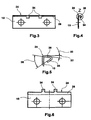
- FIG. 3 shows a flange body for an RF terminating resistor according to the invention in a plan view
- FIG. 4 shows the flange body of FIG. 3 in a side view
- FIG. 5 shows the detail Z of FIG. 4 .
- FIG. 6 shows the flange body of FIG. 3 in an unrolled representation.
- FIGS. 1-6 of the drawings in which like numerals refer to like features of the invention.
- the flange body is bent over such that the bent-over section of the flange body extends into a space between a first plane defined by the contact face of the substrate and a second plane defined by the upper face of the substrate, wherein, with one side which connects the contact face of the substrate to the upper face of the substrate and towards which the earth connection conductor track on the upper face of the substrate faces, the substrate abuts the bent-over section of the flange body.
- An electrical contact between the earth connection conductor track and the bent-over section of the flange body can be particularly easily achieved in that the bent-over section of the flange body rises from the first plane at least into the second plane or therebeyond, such that at least one section of the bent-over section of the flange body extends in the second plane adjacent to the earth connection conductor track.
- the bent-over section of the flange body has a length in a direction parallel to the first edge which corresponds to at least a width of the substrate.
- the bent-over section of the flange body has at least two noses, the separation of which in the direction parallel to the first edge of the flange body corresponds to the width of the substrate, and which, starting from the elevation, extend into a space between the first plane and the second plane, a stop is provided on both sides for the substrate, fixing a position of the substrate on the flange body even before the fastening of the substrate onto the flange body.
- the bent-over section encloses an angle of 90° with the first plane on a side facing toward the substrate.
- the bent-over section encloses an angle with the first plane on a side facing towards the substrate of less than 90°, in particular 86° to 80°.
- a layered structure which comprises a resistor layer 16 for converting RF energy into heat, an input conductor track 18 for supplying RF energy and an earth connection conductor track 20 for electrical connection to an earth contact on the flange body 10 .
- the input conductor track 18 is electrically connected to a first end of the resistor layer 16 .
- the earth connection conductor track 20 is electrically connected to a second end of the resistor layer 16 opposing the first end.
- the substrate 12 lies with a contact face 22 which faces away from the layered structure 16 , 18 , 20 on the flange body 10 .
- the flange body 10 has an edge 24 wherein the substrate 12 is arranged with the layered structure 16 , 18 , 20 mounted thereon on the flange body 10 such that the earth connection conductor track 20 faces towards said edge 24 .
- the contact face 22 of the substrate 12 defines a first plane and the upper face 14 of the substrate 12 defines a second plane.
- the predetermined section extends parallel to the edge 24 over the whole length of the edge 24 .
- This predetermined section parallel to the edge 24 can alternatively extend over just part of the length of the edge 24 , for example, over a length corresponding to the width of the substrate 12 in a direction parallel to the edge 24 .
- the bent-over section 26 of the flange body 10 is configured and bent over in such a way that the bent-over section 26 extends at least into the space between the first and second planes.
- the bent-over section 26 extends completely through the space between the first and second planes as far as the second plane and further beyond the second plane.
- the bent-over section 26 it is also possible for the bent-over section 26 to extend exactly as far as the second plane or to end within the space between the first and second planes.
- the substrate 12 makes contact with a short face 28 , which connects the upper face 14 of the substrate 12 to the contact face 22 of the substrate 12 , on the bent-over section 26 of the flange body 10 .
- the short face 28 is the face of the substrate 12 which faces towards the earth connection conductor track 20 on the upper face 14 of the substrate 12 .
- an angle between the bent-over section 26 of the flange body 10 and the upper face of the substrate 12 or between the bent-over section 26 and the plane defined by said upper face on a side facing towards the substrate 12 of less than 90°, for example 86° to 80°.
- an angle 30 between the bent-over section 26 of the flange body 10 and a perpendicular 32 to the upper face 14 of the substrate 12 has a value in the range of 4° to 10°.
- the spacing between these noses 34 in a direction parallel to the edge 24 of the flange body 10 corresponds approximately to the width of the substrate 12 in the direction parallel to the edge 24 .
- the bent-over section 26 of the flange body 10 forms the earth contact for the earth connection conductor track 20 .
- the bent-over section 26 extends into the space between the first and second planes, electrical contact can easily be created between the earth connection conductor track 20 and the bent-over section 26 without complete edge peripheral contact round the short face 28 of the substrate 12 .
- the bent-over section 26 extends above the second plane or the upper face 14 of the substrate 12 , so that the electrical contact between the earth connection conductor track 20 and the bent-over section 26 of the flange body 10 can be created directly in one plane, specifically the second plane of the upper face 14 of the substrate 12 . This simplifies the creation of the electrical contact and, simultaneously, improves the electrical properties of the RF terminating resistor, since the path of the electrical contact is as short as possible and no longer leads completely round an edge of the substrate 12 .
- a covering 38 partially covers the layered structure 16 , 18 , 20 .
- This covering is made, for example, from the same material as the substrate 12 .
- the covering 38 therefore has the same dielectric constant as the material of the substrate 12 .
- This also positively influences the electrical properties of the RF terminating resistor, since due to the dielectric ( 12 , 38 ), that is, the substrate 12 on one side and the covering 38 on the other side, which is identical on both sides, the electric field is guided close to the layered structure 16 , 18 , 20 .
- the improved design of the RF terminating resistor according to the invention, inexpensive substrates 12 , that is substrates without an edge peripheral contact, can be used.
- the overall design of the flanged load ensures the transfer of large power losses whilst maintaining the best possible broadband RF properties.
- the flange body or the flange sheet 10 with the bent-over section 26 is made entirely from one piece, for example, a press-bent part.
- the bent-over section 26 serves for the earth connection of the resistor structure 14 to the flange sheet 10 .
- the overall construction including the substrate structure 12 , 16 , 18 , 20 is intended for a broadband application with very good RF properties.
- solder joint is made from the earth connection conductor track 20 to the bent-over section 26 .
- said solder joint can be made easily, quickly and inexpensively in the second plane of the upper face 14 of the substrate 12 .
Landscapes
- Engineering & Computer Science (AREA)
- Microelectronics & Electronic Packaging (AREA)
- Physics & Mathematics (AREA)
- Electromagnetism (AREA)
- Non-Reversible Transmitting Devices (AREA)
- Details Of Resistors (AREA)
- Details Of Connecting Devices For Male And Female Coupling (AREA)
- Control Of Motors That Do Not Use Commutators (AREA)
- Amplifiers (AREA)
- Non-Adjustable Resistors (AREA)
- Shielding Devices Or Components To Electric Or Magnetic Fields (AREA)
Applications Claiming Priority (4)
| Application Number | Priority Date | Filing Date | Title |
|---|---|---|---|
| DE202006018768.5 | 2006-12-12 | ||
| DE202006018768U | 2006-12-12 | ||
| DE202006018768U DE202006018768U1 (de) | 2006-12-12 | 2006-12-12 | HF-Abschlusswiderstand in Flanschbauweise |
| PCT/EP2007/009645 WO2008071271A1 (de) | 2006-12-12 | 2007-11-07 | Hf-abschlusswiderstand in flanschbauweise |
Publications (2)
| Publication Number | Publication Date |
|---|---|
| US20100066483A1 US20100066483A1 (en) | 2010-03-18 |
| US8054157B2 true US8054157B2 (en) | 2011-11-08 |
Family
ID=37776393
Family Applications (1)
| Application Number | Title | Priority Date | Filing Date |
|---|---|---|---|
| US12/516,986 Active 2028-09-05 US8054157B2 (en) | 2006-12-12 | 2007-11-07 | RF terminating resistor of flanged construction |
Country Status (8)
| Country | Link |
|---|---|
| US (1) | US8054157B2 (de) |
| EP (1) | EP2118910B1 (de) |
| CN (1) | CN101523520A (de) |
| AT (1) | ATE463827T1 (de) |
| CA (1) | CA2666483C (de) |
| DE (2) | DE202006018768U1 (de) |
| TW (1) | TWM332921U (de) |
| WO (1) | WO2008071271A1 (de) |
Families Citing this family (1)
| Publication number | Priority date | Publication date | Assignee | Title |
|---|---|---|---|---|
| DE202006018768U1 (de) * | 2006-12-12 | 2007-02-15 | Rosenberger Hochfrequenztechnik Gmbh & Co.Kg | HF-Abschlusswiderstand in Flanschbauweise |
Citations (8)
| Publication number | Priority date | Publication date | Assignee | Title |
|---|---|---|---|---|
| EP0424536A1 (de) | 1989-02-02 | 1991-05-02 | Fujitsu Limited | Filmförmiger abschlusswiderstand für microstripleitung |
| JPH04125903A (ja) | 1990-09-17 | 1992-04-27 | Hirose Electric Co Ltd | 高周波用終端抵抗器 |
| US5896264A (en) * | 1995-02-16 | 1999-04-20 | Abb Research Ltd. | Device for current limitation and protection against short-circuit currents in an electric installation |
| JPH11186813A (ja) | 1997-12-22 | 1999-07-09 | Fuji Elelctrochem Co Ltd | マイクロ波用アイソレータ |
| US6794981B2 (en) * | 1998-12-07 | 2004-09-21 | Honeywell International Inc. | Integratable-fluid flow and property microsensor assembly |
| EP1460710A1 (de) | 2003-03-19 | 2004-09-22 | Radiall | Mikrowellenbauelement zur Dissipation oder Dämpfung von Leistung |
| DE202005013515U1 (de) | 2005-08-26 | 2005-11-03 | Rosenberger Hochfrequenztechnik Gmbh & Co. Kg | HF-Abschlusswiderstand mit einer planaren Schichtstruktur |
| US20100066483A1 (en) * | 2006-12-12 | 2010-03-18 | Rosenberger Hochfrequenztechnik Gmbh & Co. Kg | Rf terminating resistor of flanged construction |
-
2006
- 2006-12-12 DE DE202006018768U patent/DE202006018768U1/de not_active Expired - Lifetime
-
2007
- 2007-11-07 DE DE502007003432T patent/DE502007003432D1/de active Active
- 2007-11-07 EP EP07819655A patent/EP2118910B1/de active Active
- 2007-11-07 CN CNA2007800364472A patent/CN101523520A/zh active Pending
- 2007-11-07 CA CA2666483A patent/CA2666483C/en active Active
- 2007-11-07 AT AT07819655T patent/ATE463827T1/de active
- 2007-11-07 WO PCT/EP2007/009645 patent/WO2008071271A1/de not_active Ceased
- 2007-11-07 US US12/516,986 patent/US8054157B2/en active Active
- 2007-11-08 TW TW096218789U patent/TWM332921U/zh not_active IP Right Cessation
Patent Citations (8)
| Publication number | Priority date | Publication date | Assignee | Title |
|---|---|---|---|---|
| EP0424536A1 (de) | 1989-02-02 | 1991-05-02 | Fujitsu Limited | Filmförmiger abschlusswiderstand für microstripleitung |
| JPH04125903A (ja) | 1990-09-17 | 1992-04-27 | Hirose Electric Co Ltd | 高周波用終端抵抗器 |
| US5896264A (en) * | 1995-02-16 | 1999-04-20 | Abb Research Ltd. | Device for current limitation and protection against short-circuit currents in an electric installation |
| JPH11186813A (ja) | 1997-12-22 | 1999-07-09 | Fuji Elelctrochem Co Ltd | マイクロ波用アイソレータ |
| US6794981B2 (en) * | 1998-12-07 | 2004-09-21 | Honeywell International Inc. | Integratable-fluid flow and property microsensor assembly |
| EP1460710A1 (de) | 2003-03-19 | 2004-09-22 | Radiall | Mikrowellenbauelement zur Dissipation oder Dämpfung von Leistung |
| DE202005013515U1 (de) | 2005-08-26 | 2005-11-03 | Rosenberger Hochfrequenztechnik Gmbh & Co. Kg | HF-Abschlusswiderstand mit einer planaren Schichtstruktur |
| US20100066483A1 (en) * | 2006-12-12 | 2010-03-18 | Rosenberger Hochfrequenztechnik Gmbh & Co. Kg | Rf terminating resistor of flanged construction |
Also Published As
| Publication number | Publication date |
|---|---|
| ATE463827T1 (de) | 2010-04-15 |
| EP2118910B1 (de) | 2010-04-07 |
| TWM332921U (en) | 2008-05-21 |
| WO2008071271A1 (de) | 2008-06-19 |
| DE502007003432D1 (de) | 2010-05-20 |
| EP2118910A1 (de) | 2009-11-18 |
| CA2666483C (en) | 2016-01-05 |
| CA2666483A1 (en) | 2008-06-19 |
| CN101523520A (zh) | 2009-09-02 |
| DE202006018768U1 (de) | 2007-02-15 |
| US20100066483A1 (en) | 2010-03-18 |
Similar Documents
| Publication | Publication Date | Title |
|---|---|---|
| CN113169402B (zh) | 布线部件及电池模块 | |
| US7348492B1 (en) | Flexible wiring board and electrical device using the same | |
| WO2016185898A1 (ja) | 車両用窓ガラス及びアンテナ | |
| US20110227808A1 (en) | Antenna device | |
| EP2605624A1 (de) | Flexibles Flachkabel | |
| JP4897964B2 (ja) | 電流検出装置 | |
| US20150318595A1 (en) | Transmission line and electronic device | |
| US9949368B2 (en) | Resin substrate and electronic device | |
| CN105591260B (zh) | 布线部件及其制造方法、设计布线部件的方法和电子装置 | |
| US8054157B2 (en) | RF terminating resistor of flanged construction | |
| EP3035019B1 (de) | Statorschlitztemperatursensor und montageverfahren dafür | |
| KR20100132467A (ko) | 전력 반도체 모듈의 제조방법, 및 접속장치를 포함하는 전력 반도체 모듈 | |
| CN101266881B (zh) | 电子部件及其安装结构以及逆变装置 | |
| JP2015204290A (ja) | 電気加熱装置 | |
| US20060066182A1 (en) | Piezoelectric actuator | |
| US8526196B2 (en) | Method for receiving an electric/electronic component and corresponding mounting method and covering for said type of device | |
| US7358924B2 (en) | Feed network, and/or antenna having at least one antenna element and a feed network | |
| CN102548209A (zh) | 含层叠挠性互连件的柔性电路组件及具有它的连接器组件 | |
| JP2013112122A (ja) | ウインドガラス構造 | |
| US20080246691A1 (en) | Antenna apparatus | |
| EP3819935B1 (de) | Verbindungsstruktur mit einem schaltungskörper und einem leitenden körper | |
| US20220077556A1 (en) | Transmission line and electronic device | |
| JP2008271525A (ja) | 電子素子、非可逆回路素子及び固定方法 | |
| KR101003946B1 (ko) | 이동통신 단말기용 안테나 어셈블리 | |
| KR20150040512A (ko) | 길이 조절이 가능한 면상 발열체의 전극 접속용 연결단자 |
Legal Events
| Date | Code | Title | Description |
|---|---|---|---|
| AS | Assignment |
Owner name: ROSENBERGER HOCHFREQUENZTECHNIK GMBH & CO. KG,GERM Free format text: ASSIGNMENT OF ASSIGNORS INTEREST;ASSIGNOR:WEISS, FRANK;REEL/FRAME:022885/0288 Effective date: 20090518 Owner name: ROSENBERGER HOCHFREQUENZTECHNIK GMBH & CO. KG, GER Free format text: ASSIGNMENT OF ASSIGNORS INTEREST;ASSIGNOR:WEISS, FRANK;REEL/FRAME:022885/0288 Effective date: 20090518 |
|
| STCF | Information on status: patent grant |
Free format text: PATENTED CASE |
|
| FPAY | Fee payment |
Year of fee payment: 4 |
|
| MAFP | Maintenance fee payment |
Free format text: PAYMENT OF MAINTENANCE FEE, 8TH YEAR, LARGE ENTITY (ORIGINAL EVENT CODE: M1552); ENTITY STATUS OF PATENT OWNER: LARGE ENTITY Year of fee payment: 8 |
|
| FEPP | Fee payment procedure |
Free format text: 11.5 YR SURCHARGE- LATE PMT W/IN 6 MO, LARGE ENTITY (ORIGINAL EVENT CODE: M1556); ENTITY STATUS OF PATENT OWNER: LARGE ENTITY |
|
| MAFP | Maintenance fee payment |
Free format text: PAYMENT OF MAINTENANCE FEE, 12TH YEAR, LARGE ENTITY (ORIGINAL EVENT CODE: M1553); ENTITY STATUS OF PATENT OWNER: LARGE ENTITY Year of fee payment: 12 |