US9110237B2 - Method of manufacturing optical waveguide - Google Patents
Method of manufacturing optical waveguide Download PDFInfo
- Publication number
- US9110237B2 US9110237B2 US13/311,938 US201113311938A US9110237B2 US 9110237 B2 US9110237 B2 US 9110237B2 US 201113311938 A US201113311938 A US 201113311938A US 9110237 B2 US9110237 B2 US 9110237B2
- Authority
- US
- United States
- Prior art keywords
- alignment mark
- cladding layer
- formation
- opening
- mold
- Prior art date
- Legal status (The legal status is an assumption and is not a legal conclusion. Google has not performed a legal analysis and makes no representation as to the accuracy of the status listed.)
- Expired - Fee Related, expires
Links
Images


Classifications
-
- G—PHYSICS
- G02—OPTICS
- G02B—OPTICAL ELEMENTS, SYSTEMS OR APPARATUS
- G02B6/00—Light guides; Structural details of arrangements comprising light guides and other optical elements, e.g. couplings
- G02B6/10—Light guides; Structural details of arrangements comprising light guides and other optical elements, e.g. couplings of the optical waveguide type
- G02B6/12—Light guides; Structural details of arrangements comprising light guides and other optical elements, e.g. couplings of the optical waveguide type of the integrated circuit kind
- G02B6/13—Integrated optical circuits characterised by the manufacturing method
- G02B6/132—Integrated optical circuits characterised by the manufacturing method by deposition of thin films
-
- G—PHYSICS
- G03—PHOTOGRAPHY; CINEMATOGRAPHY; ANALOGOUS TECHNIQUES USING WAVES OTHER THAN OPTICAL WAVES; ELECTROGRAPHY; HOLOGRAPHY
- G03F—PHOTOMECHANICAL PRODUCTION OF TEXTURED OR PATTERNED SURFACES, e.g. FOR PRINTING, FOR PROCESSING OF SEMICONDUCTOR DEVICES; MATERIALS THEREFOR; ORIGINALS THEREFOR; APPARATUS SPECIALLY ADAPTED THEREFOR
- G03F9/00—Registration or positioning of originals, masks, frames, photographic sheets or textured or patterned surfaces, e.g. automatically
- G03F9/70—Registration or positioning of originals, masks, frames, photographic sheets or textured or patterned surfaces, e.g. automatically for microlithography
- G03F9/7003—Alignment type or strategy, e.g. leveling, global alignment
- G03F9/7042—Alignment for lithographic apparatus using patterning methods other than those involving the exposure to radiation, e.g. by stamping or imprinting
Definitions
- the present invention relates to a method of manufacturing an optical waveguide for widespread use in optical communications, optical information processing, position sensors, and other general optics.
- an optical waveguide is configured in such a manner that cores serving as a passageway for light are formed in a predetermined protruding pattern on an upper surface of an under cladding layer, and that an over cladding layer is formed so as to cover the cores.
- the under cladding layer, the cores and the over cladding layer which are made of photosensitive resin compositions and the like as materials thereof are generally formed in a stacked manner in the order named on a substrate of stainless steel foil and the like by a photolithographic method and the like.
- the optical waveguide When the optical waveguide is used as a touch position sensor for a touch panel, there are cases where a light-emitting section and a light-receiving section in the over cladding layer are formed in a lens-shaped configuration.
- a mold is used to form the over cladding layer in a specific shape in this manner.
- An exemplary method of manufacturing an optical waveguide using the aforementioned mold is as follows. First, a mold including a cavity having a mold surface complementary in shape to the surface of an over cladding layer is prepared as the aforementioned mold. Then, an under cladding layer and cores are formed in the order named on a substrate. Thereafter, a photosensitive resin composition, for example, for the formation of the over cladding layer is applied to cover the cores. Using the aforementioned mold, the applied coating layer is pressed into the shape of the over cladding layer. In that state, part of the molded coating layer is hardened to form the over cladding layer. Such a technique is disclosed, for example, in Japanese Published Patent Application No. 2008-203431.
- a mold including a through hole in communication with the aforementioned cavity is prepared as the aforementioned mold.
- the opening surface of the cavity of the mold is brought into intimate contact with the upper surface of the under cladding layer.
- a photosensitive resin composition for example, for the formation of the over cladding layer is introduced through the through hole into the cavity, and is then hardened to form the over cladding layer.
- the positioning of the aforementioned mold is generally performed with respect to an alignment mark formed to protrude from the upper surface of the under cladding layer.
- the alignment mark is generally made of a material for the formation of the cores by a photolithographic method during the formation of the cores.
- a CCD camera is used to automatically recognize the alignment mark.
- the alignment mark is formed in a cylindrical shape by a photolithographic method, for example, as shown in FIG. 6A .
- the cylindrical alignment mark 8 is photographed with the COD camera from directly above, so that a circular part of a top surface 8 a of the cylindrical alignment mark 8 is automatically recognized.
- a method of manufacturing an optical waveguide which enables a recognition device such as a CCD camera to easily recognize an alignment mark for use during the positioning of a mold when an over cladding layer is formed using the mold.
- the method of manufacturing the optical waveguide comprises the steps of: forming protruding cores and a protruding alignment mark on an upper surface of an under cladding layer by a photolithographic method; and positioning a mold for over cladding layer formation by using the alignment mark as a guide to form an over cladding layer.
- the photolithographic method employs a photomask having an opening pattern for alignment mark formation.
- the opening pattern includes an opening, and a light transmission amount reduction region provided around the opening and having an aperture ratio within a range greater than 10% and less than 80%.
- the alignment mark is formed to have a peripheral side surface in the form of an inclined surface resulting from the decrease in the amount of irradiation light transmitted through the light transmission amount reduction region, thereby enhancing the recognizability of the alignment mark with a recognition device.
- the peripheral side surface of the alignment mark is formed in the form of the inclined surface, based on the foregoing findings.
- the photomask having the opening pattern for alignment mark formation including the opening and the light transmission amount reduction region provided around the opening and having the aperture ratio within a range greater than 10% and less than 80% is used for the formation of the alignment mark
- part of the alignment mark formed by the irradiation light transmitted through the light transmission amount reduction region is formed as an inclined peripheral side surface, so that the alignment mark has the shape of a truncated cone, for example.
- the alignment mark having such an inclined peripheral side surface is easily recognizable with the recognition device such as a CCD camera.
- the irradiation light transmitted through the light transmission amount reduction region of the photomask is reduced in intensity.
- the peripheral side surface of the alignment mark which is formed by the irradiation light with the reduced intensity is formed as the inclined surface.
- the photomask having the opening pattern for alignment mark formation including the opening and the light transmission amount reduction region provided around the opening and having the aperture ratio within a range greater than 10% and less than 80% is used for the formation of the protruding alignment mark.
- This provides the peripheral side surface of the alignment mark in the form of the inclined surface, thereby producing the entire alignment mark in the shape of a truncated cone, for example.
- the recognition device such as a CCD camera
- a clear contrast is provided between the inclined surface portion of the alignment mark in the shape of the truncated cone and the horizontal portions (the top surface and the upper surface) of the alignment mark and the under cladding layer to facilitate the recognition of the alignment mark.
- This consequently prevents false recognition of the alignment mark and the time-consuming recognition thereof to achieve the efficient production of an optical waveguide having excellent alignment accuracy of the over cladding layer relative to the cores.
- the light transmission amount reduction region includes a large number of minute openings spaced at predetermined intervals.
- the aperture ratio in the light transmission amount reduction region is easily set to a predetermined value.
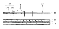
- FIGS. 1A to 1C are views schematically illustrating part of a method of manufacturing an optical waveguide according to a first preferred embodiment.
- FIG. 2A is a plan view, on an enlarged scale, schematically showing part of a photomask for use in the formation of cores and an alignment mark where the alignment mark is formed.
- FIG. 2B is a plan view, on an enlarged scale, schematically showing part of a light transmission amount reduction region of FIG. 2A .
- FIGS. 3A to 3C are views schematically illustrating part of the method of manufacturing an optical waveguide subsequent to the steps shown in FIGS. 1A to 1C .
- FIG. 4A is a view schematically illustrating an image in which an alignment mark is recognized.
- FIGS. 4B and 4C are views schematically illustrating part of the method of manufacturing an optical waveguide subsequent to the steps shown in FIGS. 3A to 3C .
- FIGS. 5A to 5C are views schematically illustrating part of a method of manufacturing an optical waveguide according to a second preferred embodiment.
- FIG. 6A is a view schematically illustrating the step of forming cores and an alignment mark in a conventional method of manufacturing an optical waveguide.
- FIG. 6B is a view schematically illustrating an image in which an alignment mark is recognized in the conventional method.
- FIGS. 1A to 1C , 2 A and 2 B, 3 A to 3 C, and 4 A to 4 C show a method of manufacturing an optical waveguide according to a first preferred embodiment.
- the method of manufacturing an optical waveguide according to the first preferred embodiment will be summarized.
- a photosensitive resin layer 2 A for the formation of cores 2 and an alignment mark 3 is formed on the upper surface of an under cladding layer 1 formed on a substrate 10 (with reference to FIGS. 1A and 1B ).
- the cores 2 and the alignment mark 3 are produced (with reference to FIG. 3A ) from the photosensitive resin layer 2 A by a photolithographic method using a photomask 20 having an opening pattern 22 for core formation and a characteristic opening pattern 23 for alignment mark formation (with reference to FIGS.
- a coating layer 4 A made of a material for the formation of an over cladding layer 4 is formed so as to cover the cores 2 and the alignment mark 3 (with reference to FIG. 3B ).
- a mold 30 is positioned using the alignment mark 3 automatically recognized with a CCD camera and the like as a guide (with reference to FIGS. 3C and 4A ). With the mold 30 positioned, the coating layer 4 A is pressed into the shape of the over cladding layer 4 by the use of the mold 30 (with reference to FIG. 4B ). Thereafter, the mold 30 is removed, so that the over cladding layer 4 is provided (with reference to FIG. 4C ). In this manner, an optical waveguide is produced on the substrate 10 .
- the method of manufacturing an optical waveguide is characterized in that the opening pattern 23 for alignment mark formation in the photomask 20 for use in the formation of the alignment mark 3 includes an opening 23 a , and a light transmission amount reduction region 23 b provided around the opening 23 a and having an aperture ratio within a range greater than 10% and less than 80% (with reference to FIGS. 1C , 2 A and 2 B).
- the use of the photomask 20 having the characteristic opening pattern 23 for alignment mark formation reduces the intensity of irradiation light L transmitted through the light transmission amount reduction region 23 b of the photomask 20 (with reference to FIG. 1C ).
- Part of the alignment mark 3 formed using the irradiation light L reduced in intensity is formed into an inclined peripheral side surface 3 b (with reference to FIG. 3A ).
- the formation of the inclined peripheral side surface 3 b provides a clear contrast between the inclined surface portion (the peripheral side surface 3 b ) and horizontal portions (a top surface 3 a and the upper surface 1 a ) of the alignment mark 3 and the under cladding layer 1 during the recognition of the alignment mark 3 with a recognition device such as a CCD camera, thereby enhancing the recognizability of the alignment mark 3 (with reference to FIG. 3C ).
- the enhancement of the recognizability of the alignment mark 3 as described above prevents false recognition of the alignment mark 3 to achieve the formation of the over cladding layer 4 in a precise position relative to the cores 2 (with reference to FIG. 4A ).
- the enhancement of the recognizability of the alignment mark 3 as described above also reduces the time required for the positioning of the mold 30 , thereby improving the productivity of optical waveguides.
- the substrate 10 of a flat shape (with reference to FIG. 1A ) for use in the formation of the under cladding layer 1 is prepared.
- a material for the formation of the substrate 10 include glass, resin such as polyethylene terephthalate (PET) and polyethylene naphthalate (PEN), metal such as stainless steel, quartz, and silicon.
- the substrate 10 has a thickness in the range of 20 ⁇ m to 1.5 mm, for example.
- the under cladding layer 1 is formed on the upper surface of the substrate 10 .
- a material for the formation of the under cladding layer 1 include thermosetting resin compositions and photosensitive resin compositions.
- thermosetting resin compositions When a thermosetting resin composition is used, the thermosetting resin composition is applied to the upper surface of the substrate 10 , and the coating layer of the thermosetting resin composition is heated, so that the under cladding layer 1 is formed.
- photosensitive resin composition on the other hand, the photosensitive resin composition is applied to the upper surface of the substrate 10 , and the coating layer of the photosensitive resin composition is exposed to irradiation light such as ultraviolet light, so that the under cladding layer 1 is formed.
- the under cladding layer 1 has a thickness in the range of 5 to 60 ⁇ m, for example.
- a photosensitive resin composition serving as a material for the formation of the cores 2 and the alignment mark 3 (with reference to FIG. 3A ) is applied to the upper surface of the under cladding layer 1 to form the photosensitive resin layer 2 A.
- the photomask 20 having the opening patterns 22 and 23 corresponding to the patterns of the cores 2 and the alignment mark 3 is placed over the photosensitive resin layer 2 A.
- the photosensitive resin layer 2 A is exposed to irradiation light L such as ultraviolet light through the photomask 20 .
- FIG. 2A is a plan view, on an enlarged scale, of part of the photomask 20 .
- the photomask 20 has the opening pattern 23 for alignment mark formation which includes the opening 23 a , and the light transmission amount reduction region 23 b provided around the opening 23 a and having an aperture ratio within a range greater than 10% and less than 80%, as mentioned above.
- the opening 23 a of the opening pattern 23 for alignment mark formation is of a circular configuration
- the light transmission amount reduction region 23 b provided around the opening 23 a is of an annular ring-shaped configuration.
- the light transmission amount reduction region 23 b according to the first preferred embodiment includes a large number of quadrilateral minute openings 23 c spaced at predetermined intervals.
- the aperture ratio in the light transmission amount reduction region 23 b is set at a predetermined constant value within the aforementioned range.
- the peripheral side surface 3 b of the alignment mark 3 formed in this manner is an inclined surface because the irradiation light L reduced in intensity by being transmitted through the light transmission amount reduction region 23 b of the photomask 20 is used for the formation of the peripheral side surface 3 b .
- the alignment mark 3 is in the shape of a truncated cone.
- the light transmission amount reduction region 23 b of the photomask 20 includes the large number of minute openings 23 c spaced at predetermined intervals as described above to thereby have an aperture ratio within a range greater than 10% and less than 80%. This is because, when the aperture ratio falls outside the aforementioned range, the peripheral side surface 3 b of the alignment mark 3 is not formed as the inclined surface, in which case a clear contrast is not obtained in a subsequent step of recognizing the alignment mark 3 , so that the recognizability of the alignment mark 3 is not improved.
- a resin composition serving as a material for the formation of the over cladding layer 4 is applied so as to cover the cores 2 and the alignment mark 3 to form the coating layer 4 A of the resin composition, as shown in FIG. 3B .
- the material for the formation of the over cladding layer 4 include thermosetting resin compositions and photosensitive resin compositions similar to those for the under cladding layer 1 .
- the coating layer 4 A is permeable to light because it is necessary to automatically recognize the alignment mark 3 through the coating layer 4 A with a recognition device such as a CCD camera from directly above in the next step.
- the mold 30 including a cavity 31 having a mold surface complementary in shape to the surface of the over cladding layer 4 is prepared, as shown in FIG. 3C .
- part of the mold surface of the mold 30 corresponding to the tips of the cores 2 is in the form of a curved lens surface 31 a .
- the process of curing the coating layer 4 A differs depending on the material for the formation of the over cladding layer 4 , which will be described below.
- the mold 30 used herein is made of quartz, for example, which is permeable to light because of the necessity to allow irradiation light for exposure to pass through.
- the mold 30 used herein is made of quartz, polymer and metal, for example.
- the alignment mark 3 is automatically recognized through the coating layer 4 A with a recognition device such as a CCD camera from directly above.
- the mold 30 is positioned with respect to the position of the automatically recognized alignment mark 3 .
- an image obtained by the recognition device shows a clear contrast between the inclined portion (the peripheral side surface 3 b ) of the alignment mark 3 and the horizontal portions (the top surface 3 a and the upper surface 1 a ) of the alignment mark 3 and the under cladding layer 1 , as shown in FIG. 4A , regardless of whether the lighting during the automatic recognition is coaxial overhead illumination or illumination at other lighting angles.
- the peripheral edge 3 c of the alignment mark 3 (a boundary line between the alignment mark 3 and its surrounding part) in the image becomes clear, so that the alignment mark 3 is easily recognized with the recognition device.
- the coating layer 4 A is pressed into the shape of the over cladding layer 4 by the use of the mold 30 , as shown in FIG. 4B .
- the molded part of the coating layer 4 A is cured to form the over cladding layer 4 .
- the curing of the coating layer 4 A is done by heating the coating layer 4 A when a thermosetting resin composition is used as the material for the formation of the over cladding layer 4 , and is done by exposing the coating layer 4 A with irradiation light such as ultraviolet light through the mold 30 when a photosensitive resin composition is used as the material for the formation of the over cladding layer 4 .
- the mold 30 is removed, as shown in FIG. 4C .
- This provides the over cladding layer 4 properly positioned relative to the cores 2 .
- an optical waveguide including the under cladding layer 1 , the cores 2 , the alignment mark 3 and the over cladding layer 4 is produced on the upper surface of the substrate 10 .
- the opening 23 a of a circular configuration in the center of the opening pattern 23 for alignment mark formation in the photomask 20 is used to produce the alignment mark 3 in the shape of a truncated cone.
- the opening 23 a and the alignment mark 3 may be of other configurations.
- the opening 23 a of a polygonal configuration, such as triangular and quadrilateral configurations, or of a cross-shaped configuration may be used to produce the alignment mark 3 in the shape of a truncated polygonal pyramid, such as truncated triangular and quadrangular pyramids, or in the shape of a truncated cross-shaped pyramid.
- the large number of minute openings 23 c formed in the light transmission amount reduction region 23 b around the opening 23 a is quadrilateral in shape according to the first preferred embodiment, but may be of other configurations.
- the minute openings 23 c may be of a circular configuration or a polygonal configuration, such as triangular and pentagonal configurations.
- the aperture ratio in the light transmission amount reduction region 23 b is set at a predetermined constant value within a range greater than 10% and less than 80% according to the first preferred embodiment. However, the aperture ratio may be set so as to decrease gradually within the aforementioned range toward the outside of the light transmission amount reduction region 23 b.
- a mold 40 including a cavity 41 in communication with through holes 42 may be used, as shown in FIG. 5A , in place of the mold 30 for over cladding layer formation in the first preferred embodiment.
- the formation of the over cladding layer 4 by the use of the mold 40 is as follows. As in the first preferred embodiment, the mold 40 is positioned with respect to the position of the alignment mark 3 automatically recognized with a recognition device such as a CCD camera, as shown in FIG. 5B . In this state, the opening surface of the cavity 41 of the mold 40 is brought into intimate contact with the upper surface of the under cladding layer 1 . In that state, as shown in FIG. 5C , the material for the formation of the over cladding layer 4 is introduced through the through holes 42 into the cavity 41 , and is then cured. This provides the over cladding layer 4 .
- Component A solid epoxy resin: 70 parts by weight of an epoxy resin having an aromatic ring skeleton (Epicoat 1002 available from Mitsubishi Chemical Corporation).
- Component B solid epoxy resin: 30 parts by weight of an epoxy resin having an alicyclic skeleton (EHPE 3150 available from Daicel Chemical Industries, Ltd.).
- Component C photo-acid generator: two parts by weight of a 50% propione carbonate solution of a triaryl sulfonium salt (CPI-200K available from San-Apro Ltd.).
- a material (a photosensitive resin composition) for the formation of an under cladding layer was prepared by stirring (at a temperature of 80° C. at 250 rpm for three hours) to dissolve these components A to C in 55 parts by weight of ethyl lactate (available from Musashino Chemical Laboratory, Ltd.).
- Component D 100 parts by weight of O-cresol novolac glycidyl ether (YDCN-700-10 available from Nippon Steel Chemical Co., Ltd.).
- a material (a photosensitive resin composition) for the formation of cores was prepared by stirring (at a temperature of 80° C. at 250 rpm for three hours) to dissolve the component D and one part by weight of the aforementioned component C in 60 parts by weight of ethyl lactate (available from Musashino Chemical Laboratory, Ltd.).
- the material for the formation of the under cladding layer was applied to a surface of SUS304 foil (available from Toyo Seihaku Co., Ltd. and having a thickness of 20 ⁇ m) with a spin coater (1X-DX2 available from Mikasa Co., Ltd.). Thereafter, a drying process was performed at 130° C. for 10 minutes to form a photosensitive resin layer.
- an exposure machine MA-60F available from Mikasa Co., Ltd.
- an ultra-high-pressure mercury-vapor lamp USH-250D available from Ushio Inc.
- a heating treatment was performed at 130° C. for 10 minutes to form the under cladding layer (with reference to FIG. 1A ).
- a photomask having opening patterns corresponding to the patterns of the cores and an alignment mark was prepared.
- the opening pattern for alignment mark formation included a circular opening having a diameter of 0.6 mm, and an annular ring-shaped light transmission amount reduction region provided around the opening and having an outer diameter of 0.8 mm.
- the light transmission amount reduction region included a large number of quadrilateral minute openings having dimensions of 3 by 3 ⁇ m and spaced at intervals of 7 ⁇ m, thereby to have an aperture ratio of 15% (with reference to FIGS. 2A and 2B ).
- the material for the formation of the cores was applied to the upper surface of the under cladding layer with the aforementioned spin coater. Thereafter, a drying process was performed at 130° C. for five minutes to form a photosensitive resin layer (with reference to FIG. 1B ). Then, the aforementioned exposure machine and the aforementioned ultra-high-pressure mercury-vapor lamp were used to irradiate the photosensitive resin layer with ultraviolet light (having a wavelength of 365 nm), thereby exposing the photosensitive resin layer to the ultraviolet light at an integrated dose of 4000 mJ/cm 2 (with reference to FIG. 1C ). Subsequently, a heating treatment was performed at 130° C. for 15 minutes.
- the photomask used in Inventive Example 1 had an opening pattern for alignment mark formation in which a light transmission amount reduction region included a large number of quadrilateral minute openings having dimensions of 7 by 7 ⁇ m and spaced at intervals of 11 ⁇ m, thereby to have an aperture ratio of 40%. Except for these differences, the cores and the alignment mark in Inventive Example 2 were formed on the upper surface of the under cladding layer in a manner similar to that in Inventive Example 1 described above.
- the photomask used in Inventive Example 1 had an opening pattern for alignment mark formation in which a light transmission amount reduction region included a large number of quadrilateral minute openings having dimensions of 10 by 10 ⁇ m and spaced at intervals of 13 um, thereby to have an aperture ratio of 60%. Except for these differences, the cores and the alignment mark in Inventive Example 3 were formed on the upper surface of the under cladding layer in a manner similar to that in Inventive Example 1 described above.
- the photomask used in Inventive Example 1 had an opening pattern for alignment mark formation in which a light transmission amount reduction region included a large number of quadrilateral minute openings having dimensions of 3 by 3 ⁇ m and spaced at intervals of 9 ⁇ m, thereby to have an aperture ratio of 10%. Except for these differences, the cores and the alignment mark in Comparative Example 1 were formed on the upper surface of the under cladding layer in a manner similar to that in Inventive Example 1 described above.
- the photomask used in Inventive Example 1 had an opening pattern for alignment mark formation in which a light transmission amount reduction region included a large number of quadrilateral minute openings having dimensions of 10 by 10 ⁇ m and spaced at intervals of 12 ⁇ m, thereby to have an aperture ratio of 80%. Except for these differences, the cores and the alignment mark in Comparative Example 2 were formed on the upper surface of the under cladding layer in a manner similar to that in Inventive Example 1 described above.
- a CCD camera (IV-S210X available from Sharp Manufacturing Systems Corporation) was used to automatically recognize the alignment marks in Inventive Examples 1 to 3 and Comparative Examples 1 and 2.
- images obtained by the CCD camera were gray-scale images, and the alignment marks were detected using a circular search area having a diameter of 0.6 mm.
- alignment marks that were automatically recognized within one second were evaluated as being “good” and indicated by open circles in Table 1 below, and alignment marks that were not automatically recognized after five seconds were evaluated as being “unacceptable” and indicated by crosses in Table 1 below.
- Table 1 show that the alignment marks in Inventive Examples 1 to 3 each formed using the photomask having the opening pattern for alignment mark formation in which the light transmission amount reduction region has an aperture ratio within a range greater than 10% and less than 80% are high in recognizability with the CCD camera, as compared with the alignment marks in Comparative Examples 1 and 2 each formed using the photomask in which the light transmission amount reduction region has an aperture ratio falling outside the aforementioned range.
- Results similar to those described above were produced when the configuration of the opening of the opening pattern for alignment mark formation in each of the photomasks was changed to a triangular configuration, a quadrilateral configuration and a cross-shaped configuration to produce the alignment mark in the shape of a truncated triangular pyramid, a truncated quadrangular pyramid and a truncated cross-shaped pyramid.
- results similar to those described above were produced when the alignment mark was formed with various configurations and sizes of the minute openings formed in the light transmission amount reduction region.
- the results showed that the recognizability of the alignment mark with the CCD camera was not influenced by variations in the configuration and size of the minute openings when the aperture ratio remained the same.
- the method of manufacturing an optical waveguide is applicable to instances where the over cladding layer is formed by positioning the mold with respect to the alignment mark.
Landscapes
- Physics & Mathematics (AREA)
- General Physics & Mathematics (AREA)
- Engineering & Computer Science (AREA)
- Microelectronics & Electronic Packaging (AREA)
- Optics & Photonics (AREA)
- Optical Integrated Circuits (AREA)
Applications Claiming Priority (2)
| Application Number | Priority Date | Filing Date | Title |
|---|---|---|---|
| JP2010-285791 | 2010-12-22 | ||
| JP2010285791A JP5653745B2 (ja) | 2010-12-22 | 2010-12-22 | 光導波路の製法 |
Publications (2)
| Publication Number | Publication Date |
|---|---|
| US20120164313A1 US20120164313A1 (en) | 2012-06-28 |
| US9110237B2 true US9110237B2 (en) | 2015-08-18 |
Family
ID=46317343
Family Applications (1)
| Application Number | Title | Priority Date | Filing Date |
|---|---|---|---|
| US13/311,938 Expired - Fee Related US9110237B2 (en) | 2010-12-22 | 2011-12-06 | Method of manufacturing optical waveguide |
Country Status (4)
| Country | Link |
|---|---|
| US (1) | US9110237B2 (ja) |
| JP (1) | JP5653745B2 (ja) |
| CN (1) | CN102565941B (ja) |
| TW (1) | TWI504950B (ja) |
Cited By (1)
| Publication number | Priority date | Publication date | Assignee | Title |
|---|---|---|---|---|
| US20140311780A1 (en) * | 2013-04-23 | 2014-10-23 | Ibiden Co., Ltd. | Electronic component, method for manufacturing the same and method for manufacturing multilayer printed wiring board |
Families Citing this family (3)
| Publication number | Priority date | Publication date | Assignee | Title |
|---|---|---|---|---|
| CN103966546B (zh) * | 2014-04-29 | 2016-03-16 | 京东方科技集团股份有限公司 | 一种金属掩膜板 |
| CN104977653B (zh) * | 2015-06-18 | 2018-03-23 | 湖南晶图科技有限公司 | 一种plc波导微耦合镜面的加工方法 |
| JP6565973B2 (ja) | 2017-06-29 | 2019-08-28 | 日亜化学工業株式会社 | 実装用部品、それを用いた半導体装置及びその製造方法 |
Citations (21)
| Publication number | Priority date | Publication date | Assignee | Title |
|---|---|---|---|---|
| CN1327261A (zh) | 2000-06-02 | 2001-12-19 | 国际商业机器公司 | 改进工艺窗口制作全自对准薄膜场效应晶体管的方法 |
| US20020074308A1 (en) * | 2000-02-03 | 2002-06-20 | Beguin Alain M.J. | High precision alignment of optical waveguide features |
| US20030180628A1 (en) | 2002-03-22 | 2003-09-25 | Chih-Ming Lai | Process of manufacturing a diffusive direct reflector using gray tone exposure |
| US20050118515A1 (en) * | 2003-01-23 | 2005-06-02 | Progler Christopher J. | Binary half tone photomasks and microscopic three-dimensional devices and method of fabricating the same |
| US20050225693A1 (en) | 2004-03-04 | 2005-10-13 | Seiko Epson Corporation | Manufacturing method for fine structure element, fine structure element manufactured by the method, spatial light modulator, and projector |
| CN1764516A (zh) | 2004-03-04 | 2006-04-26 | 精工爱普生株式会社 | 微细结构元件的制造方法及其应用 |
| US20070031761A1 (en) * | 2002-10-16 | 2007-02-08 | Georgia Tech Research Corp. | Polymers, methods of use thereof, and methods of decomposition thereof |
| JP2007210126A (ja) | 2006-02-07 | 2007-08-23 | Pioneer Electronic Corp | 転写型およびこの転写型のアライメント方法 |
| US20080013903A1 (en) * | 2006-07-13 | 2008-01-17 | Fuji Xerox Co., Ltd. | Optical waveguide and method of manufacturing the same |
| CN101122739A (zh) | 2007-08-31 | 2008-02-13 | 中国科学院光电技术研究所 | 一种基于负折射率透镜的亚波长连续面形微结构制备方法 |
| JP2008076824A (ja) | 2006-09-22 | 2008-04-03 | Seiko Epson Corp | 液晶装置の製造方法 |
| US20080198144A1 (en) | 2007-02-19 | 2008-08-21 | Nitto Denko Corporation | Optical waveguide for touch panel |
| US20080277809A1 (en) | 2007-05-08 | 2008-11-13 | Nitto Denko Corporation | Manufacturing method of optical waveguide |
| US20090140438A1 (en) | 2007-12-03 | 2009-06-04 | Semiconductor Energy Laboratory Co., Ltd. | Semiconductor device and manufacturing method thereof |
| US20090202737A1 (en) * | 2008-02-07 | 2009-08-13 | Nitto Denko Corporation | Manufacturing method of optical waveguide for touch panel |
| US20090269704A1 (en) | 2008-04-24 | 2009-10-29 | Nitto Denko Corporation | Manufacturing method of opto-electric hybrid board |
| US20100027937A1 (en) | 2008-07-29 | 2010-02-04 | Nitto Denko Corporation | Three-dimensional sensor optical waveguide, and three-dimensional sensor employing the same |
| JP2010097192A (ja) | 2008-09-18 | 2010-04-30 | Dainippon Printing Co Ltd | 有機エレクトロルミネッセンス表示装置用カラーフィルタおよび有機エレクトロルミネッセンス表示装置 |
| US20100129026A1 (en) | 2008-11-27 | 2010-05-27 | Nitto Denko Corporation | Opto-electric hybrid board and manufacturing method thereof |
| TW201040599A (en) | 2009-03-18 | 2010-11-16 | Asahi Glass Co Ltd | Optical waveguide |
| US20110262860A1 (en) * | 2010-04-22 | 2011-10-27 | Board Of Regents, The University Of Texas | Novel dual-tone resist formulations and methods |
-
2010
- 2010-12-22 JP JP2010285791A patent/JP5653745B2/ja not_active Expired - Fee Related
-
2011
- 2011-12-06 US US13/311,938 patent/US9110237B2/en not_active Expired - Fee Related
- 2011-12-12 CN CN201110411253.4A patent/CN102565941B/zh not_active Expired - Fee Related
- 2011-12-15 TW TW100146469A patent/TWI504950B/zh not_active IP Right Cessation
Patent Citations (33)
| Publication number | Priority date | Publication date | Assignee | Title |
|---|---|---|---|---|
| US20020074308A1 (en) * | 2000-02-03 | 2002-06-20 | Beguin Alain M.J. | High precision alignment of optical waveguide features |
| CN1327261A (zh) | 2000-06-02 | 2001-12-19 | 国际商业机器公司 | 改进工艺窗口制作全自对准薄膜场效应晶体管的方法 |
| US6403407B1 (en) | 2000-06-02 | 2002-06-11 | International Business Machines Corporation | Method of forming fully self-aligned TFT with improved process window |
| US20030180628A1 (en) | 2002-03-22 | 2003-09-25 | Chih-Ming Lai | Process of manufacturing a diffusive direct reflector using gray tone exposure |
| JP2003287608A (ja) | 2002-03-22 | 2003-10-10 | Ind Technol Res Inst | 拡散反射板の製法 |
| US6773870B2 (en) | 2002-03-22 | 2004-08-10 | Industrial Technology Research Institute | Process of manufacturing a diffusive direct reflector using gray tone exposure |
| US20070031761A1 (en) * | 2002-10-16 | 2007-02-08 | Georgia Tech Research Corp. | Polymers, methods of use thereof, and methods of decomposition thereof |
| US20050118515A1 (en) * | 2003-01-23 | 2005-06-02 | Progler Christopher J. | Binary half tone photomasks and microscopic three-dimensional devices and method of fabricating the same |
| US20050225693A1 (en) | 2004-03-04 | 2005-10-13 | Seiko Epson Corporation | Manufacturing method for fine structure element, fine structure element manufactured by the method, spatial light modulator, and projector |
| CN1764516A (zh) | 2004-03-04 | 2006-04-26 | 精工爱普生株式会社 | 微细结构元件的制造方法及其应用 |
| JP2007210126A (ja) | 2006-02-07 | 2007-08-23 | Pioneer Electronic Corp | 転写型およびこの転写型のアライメント方法 |
| US20080013903A1 (en) * | 2006-07-13 | 2008-01-17 | Fuji Xerox Co., Ltd. | Optical waveguide and method of manufacturing the same |
| JP2008076824A (ja) | 2006-09-22 | 2008-04-03 | Seiko Epson Corp | 液晶装置の製造方法 |
| JP2008203431A (ja) | 2007-02-19 | 2008-09-04 | Nitto Denko Corp | タッチパネル用光導波路 |
| US20080198144A1 (en) | 2007-02-19 | 2008-08-21 | Nitto Denko Corporation | Optical waveguide for touch panel |
| US20080277809A1 (en) | 2007-05-08 | 2008-11-13 | Nitto Denko Corporation | Manufacturing method of optical waveguide |
| JP2008281654A (ja) | 2007-05-08 | 2008-11-20 | Nitto Denko Corp | 光導波路の製造方法 |
| CN101122739A (zh) | 2007-08-31 | 2008-02-13 | 中国科学院光电技术研究所 | 一种基于负折射率透镜的亚波长连续面形微结构制备方法 |
| US20090140438A1 (en) | 2007-12-03 | 2009-06-04 | Semiconductor Energy Laboratory Co., Ltd. | Semiconductor device and manufacturing method thereof |
| CN101452906A (zh) | 2007-12-03 | 2009-06-10 | 株式会社半导体能源研究所 | 半导体器件及其制造方法 |
| US20090202737A1 (en) * | 2008-02-07 | 2009-08-13 | Nitto Denko Corporation | Manufacturing method of optical waveguide for touch panel |
| JP2009186834A (ja) | 2008-02-07 | 2009-08-20 | Nitto Denko Corp | タッチパネル用光導波路の製造方法 |
| CN101533127A (zh) | 2008-02-07 | 2009-09-16 | 日东电工株式会社 | 触摸屏用光波导的制造方法 |
| JP2009265342A (ja) | 2008-04-24 | 2009-11-12 | Nitto Denko Corp | 光電気混載基板の製造方法 |
| US20090269704A1 (en) | 2008-04-24 | 2009-10-29 | Nitto Denko Corporation | Manufacturing method of opto-electric hybrid board |
| US20100027937A1 (en) | 2008-07-29 | 2010-02-04 | Nitto Denko Corporation | Three-dimensional sensor optical waveguide, and three-dimensional sensor employing the same |
| JP2010032378A (ja) | 2008-07-29 | 2010-02-12 | Nitto Denko Corp | 3次元センサ用光導波路およびそれを用いた3次元センサ |
| JP2010097192A (ja) | 2008-09-18 | 2010-04-30 | Dainippon Printing Co Ltd | 有機エレクトロルミネッセンス表示装置用カラーフィルタおよび有機エレクトロルミネッセンス表示装置 |
| US20100129026A1 (en) | 2008-11-27 | 2010-05-27 | Nitto Denko Corporation | Opto-electric hybrid board and manufacturing method thereof |
| JP2010128200A (ja) | 2008-11-27 | 2010-06-10 | Nitto Denko Corp | 光電気混載基板およびその製造方法 |
| TW201040599A (en) | 2009-03-18 | 2010-11-16 | Asahi Glass Co Ltd | Optical waveguide |
| US20120002932A1 (en) | 2009-03-18 | 2012-01-05 | Asahi Glass Company, Limited | Optical waveguide |
| US20110262860A1 (en) * | 2010-04-22 | 2011-10-27 | Board Of Regents, The University Of Texas | Novel dual-tone resist formulations and methods |
Non-Patent Citations (7)
| Title |
|---|
| Chinese Office Action dated Jul. 3, 2014, issued in corresponding Chinese Application No. 201110411253.4; w/ English Translation (14 pages). |
| Chinese Office Action dated Mar. 20, 2015, issued in corresponding CN Patent Application No. 2011104112534 with English translation (16 pages). |
| Japanese Decision of Rejection dated Jul. 1, 2014, issued in Japanese Patent Application No. 2010-285791, w/ English translation (2 pages). |
| Japanese Decision of Rejection of the Amendment dated Jul. 1, 2014, issued in Japanese Patent Application No. 2010-285791, w/English translation (6 pages). |
| Japanese Office Action dated Mar. 12, 2013, issued in corresponding Japanese Patent Application No. 2010-285791, w/ English translation. |
| Japanese Office Action dated Nov. 5, 2013, corresponding to Japanese Application No. 2010-285791 w/English Translation. (6 pages). |
| Office Action dated Jan. 26, 2015, issued in corresponding Taiwanese Application No. 100146469, w/English translation. (7 pages). |
Cited By (2)
| Publication number | Priority date | Publication date | Assignee | Title |
|---|---|---|---|---|
| US20140311780A1 (en) * | 2013-04-23 | 2014-10-23 | Ibiden Co., Ltd. | Electronic component, method for manufacturing the same and method for manufacturing multilayer printed wiring board |
| US9433085B2 (en) * | 2013-04-23 | 2016-08-30 | Ibiden Co., Ltd. | Electronic component, method for manufacturing the same and method for manufacturing multilayer printed wiring board |
Also Published As
| Publication number | Publication date |
|---|---|
| CN102565941B (zh) | 2016-01-20 |
| CN102565941A (zh) | 2012-07-11 |
| TWI504950B (zh) | 2015-10-21 |
| JP2012133171A (ja) | 2012-07-12 |
| US20120164313A1 (en) | 2012-06-28 |
| TW201234061A (en) | 2012-08-16 |
| JP5653745B2 (ja) | 2015-01-14 |
Similar Documents
| Publication | Publication Date | Title |
|---|---|---|
| KR100233417B1 (ko) | 마이크로렌즈 형성방법 | |
| US9110237B2 (en) | Method of manufacturing optical waveguide | |
| US20080277809A1 (en) | Manufacturing method of optical waveguide | |
| JP2006072349A (ja) | 直接的にパターン化可能なマイクロレンズ | |
| TW200508811A (en) | Exposure method, exposure device, and device manufacturing method | |
| EP1988414A1 (en) | Optical waveguide | |
| CN101430401B (zh) | 光波导路装置的制造方法以及由此获得的光波导路装置 | |
| KR100687015B1 (ko) | 웨이퍼 주변 노광 장치 및 웨이퍼 주변 노광 방법 | |
| EP2051117A2 (en) | Film-shaped optical waveguide production method | |
| US20100068653A1 (en) | Manufacturing method of optical waveguide device | |
| CN104779145B (zh) | 掩膜板及其制备方法 | |
| JP4629473B2 (ja) | 固体撮像素子の製造方法 | |
| US8538220B2 (en) | Manufacturing method of optical waveguide device and optical waveguide device obtained thereby | |
| CN101408643B (zh) | 光波导器件及其制造方法 | |
| KR20100000706A (ko) | 미세 패턴 형성 방법 | |
| JP2008090303A (ja) | レジストの最適化によるウオータマーク欠陥の低減 | |
| JP2004079590A (ja) | 不要膜除去装置および不要膜除去方法、並びにフォトマスクブランク製造方法 | |
| JP2008298878A (ja) | 光導波路デバイス | |
| CN108922989B (zh) | 显示面板及其制备方法、显示装置 | |
| US20080274273A1 (en) | Manufacturing method of optical waveguide | |
| CN109143795B (zh) | 一种光刻镜片的制作方法和镜头 | |
| KR100702792B1 (ko) | 반도체 제조용 노광 장치 | |
| US8472005B2 (en) | Methodology for implementing enhanced optical lithography for hole patterning in semiconductor fabrication | |
| KR20040008400A (ko) | 반도체 소자의 패턴 형성 방법 | |
| JP2000173916A (ja) | 照明装置及びそれを用いた投影露光装置 |
Legal Events
| Date | Code | Title | Description |
|---|---|---|---|
| AS | Assignment |
Owner name: NITTO DENKO CORPORATION, JAPAN Free format text: ASSIGNMENT OF ASSIGNORS INTEREST;ASSIGNORS:SHIBATA, NAOKI;NAITO, RYUSUKE;MIZUTANI, TORU;SIGNING DATES FROM 20111020 TO 20111021;REEL/FRAME:027369/0014 |
|
| STCF | Information on status: patent grant |
Free format text: PATENTED CASE |
|
| FEPP | Fee payment procedure |
Free format text: PAYOR NUMBER ASSIGNED (ORIGINAL EVENT CODE: ASPN); ENTITY STATUS OF PATENT OWNER: LARGE ENTITY |
|
| FEPP | Fee payment procedure |
Free format text: MAINTENANCE FEE REMINDER MAILED (ORIGINAL EVENT CODE: REM.); ENTITY STATUS OF PATENT OWNER: LARGE ENTITY |
|
| LAPS | Lapse for failure to pay maintenance fees |
Free format text: PATENT EXPIRED FOR FAILURE TO PAY MAINTENANCE FEES (ORIGINAL EVENT CODE: EXP.); ENTITY STATUS OF PATENT OWNER: LARGE ENTITY |
|
| STCH | Information on status: patent discontinuation |
Free format text: PATENT EXPIRED DUE TO NONPAYMENT OF MAINTENANCE FEES UNDER 37 CFR 1.362 |
|
| FP | Lapsed due to failure to pay maintenance fee |
Effective date: 20190818 |