US9155193B2 - Flexible circuit board and its method for production - Google Patents
Flexible circuit board and its method for production Download PDFInfo
- Publication number
- US9155193B2 US9155193B2 US13/641,769 US201013641769A US9155193B2 US 9155193 B2 US9155193 B2 US 9155193B2 US 201013641769 A US201013641769 A US 201013641769A US 9155193 B2 US9155193 B2 US 9155193B2
- Authority
- US
- United States
- Prior art keywords
- circuit board
- flexible circuit
- spiral part
- insulating film
- wiring layer
- Prior art date
- Legal status (The legal status is an assumption and is not a legal conclusion. Google has not performed a legal analysis and makes no representation as to the accuracy of the status listed.)
- Active, expires
Links
Images



Classifications
-
- H—ELECTRICITY
- H05—ELECTRIC TECHNIQUES NOT OTHERWISE PROVIDED FOR
- H05K—PRINTED CIRCUITS; CASINGS OR CONSTRUCTIONAL DETAILS OF ELECTRIC APPARATUS; MANUFACTURE OF ASSEMBLAGES OF ELECTRICAL COMPONENTS
- H05K1/00—Printed circuits
- H05K1/02—Details
- H05K1/0277—Bendability or stretchability details
- H05K1/028—Bending or folding regions of flexible printed circuits
-
- H—ELECTRICITY
- H05—ELECTRIC TECHNIQUES NOT OTHERWISE PROVIDED FOR
- H05K—PRINTED CIRCUITS; CASINGS OR CONSTRUCTIONAL DETAILS OF ELECTRIC APPARATUS; MANUFACTURE OF ASSEMBLAGES OF ELECTRICAL COMPONENTS
- H05K1/00—Printed circuits
- H05K1/02—Details
- H05K1/0213—Electrical arrangements not otherwise provided for
- H05K1/0216—Reduction of cross-talk, noise or electromagnetic interference
- H05K1/0218—Reduction of cross-talk, noise or electromagnetic interference by printed shielding conductors, ground planes or power plane
-
- H—ELECTRICITY
- H05—ELECTRIC TECHNIQUES NOT OTHERWISE PROVIDED FOR
- H05K—PRINTED CIRCUITS; CASINGS OR CONSTRUCTIONAL DETAILS OF ELECTRIC APPARATUS; MANUFACTURE OF ASSEMBLAGES OF ELECTRICAL COMPONENTS
- H05K1/00—Printed circuits
- H05K1/18—Printed circuits structurally associated with non-printed electric components
- H05K1/189—Printed circuits structurally associated with non-printed electric components characterised by the use of flexible or folded printed circuits
-
- H—ELECTRICITY
- H05—ELECTRIC TECHNIQUES NOT OTHERWISE PROVIDED FOR
- H05K—PRINTED CIRCUITS; CASINGS OR CONSTRUCTIONAL DETAILS OF ELECTRIC APPARATUS; MANUFACTURE OF ASSEMBLAGES OF ELECTRICAL COMPONENTS
- H05K2201/00—Indexing scheme relating to printed circuits covered by H05K1/00
- H05K2201/01—Dielectrics
- H05K2201/0104—Properties and characteristics in general
- H05K2201/0129—Thermoplastic polymer, e.g. auto-adhesive layer; Shaping of thermoplastic polymer
-
- H—ELECTRICITY
- H05—ELECTRIC TECHNIQUES NOT OTHERWISE PROVIDED FOR
- H05K—PRINTED CIRCUITS; CASINGS OR CONSTRUCTIONAL DETAILS OF ELECTRIC APPARATUS; MANUFACTURE OF ASSEMBLAGES OF ELECTRICAL COMPONENTS
- H05K2201/00—Indexing scheme relating to printed circuits covered by H05K1/00
- H05K2201/01—Dielectrics
- H05K2201/0137—Materials
- H05K2201/0141—Liquid crystal polymer [LCP]
-
- H—ELECTRICITY
- H05—ELECTRIC TECHNIQUES NOT OTHERWISE PROVIDED FOR
- H05K—PRINTED CIRCUITS; CASINGS OR CONSTRUCTIONAL DETAILS OF ELECTRIC APPARATUS; MANUFACTURE OF ASSEMBLAGES OF ELECTRICAL COMPONENTS
- H05K2201/00—Indexing scheme relating to printed circuits covered by H05K1/00
- H05K2201/05—Flexible printed circuits [FPCs]
- H05K2201/051—Rolled
-
- H—ELECTRICITY
- H05—ELECTRIC TECHNIQUES NOT OTHERWISE PROVIDED FOR
- H05K—PRINTED CIRCUITS; CASINGS OR CONSTRUCTIONAL DETAILS OF ELECTRIC APPARATUS; MANUFACTURE OF ASSEMBLAGES OF ELECTRICAL COMPONENTS
- H05K2201/00—Indexing scheme relating to printed circuits covered by H05K1/00
- H05K2201/05—Flexible printed circuits [FPCs]
- H05K2201/057—Shape retainable
-
- H—ELECTRICITY
- H05—ELECTRIC TECHNIQUES NOT OTHERWISE PROVIDED FOR
- H05K—PRINTED CIRCUITS; CASINGS OR CONSTRUCTIONAL DETAILS OF ELECTRIC APPARATUS; MANUFACTURE OF ASSEMBLAGES OF ELECTRICAL COMPONENTS
- H05K2203/00—Indexing scheme relating to apparatus or processes for manufacturing printed circuits covered by H05K3/00
- H05K2203/11—Treatments characterised by their effect, e.g. heating, cooling, roughening
- H05K2203/1105—Heating or thermal processing not related to soldering, firing, curing or laminating, e.g. for shaping the substrate or during finish plating
-
- Y—GENERAL TAGGING OF NEW TECHNOLOGICAL DEVELOPMENTS; GENERAL TAGGING OF CROSS-SECTIONAL TECHNOLOGIES SPANNING OVER SEVERAL SECTIONS OF THE IPC; TECHNICAL SUBJECTS COVERED BY FORMER USPC CROSS-REFERENCE ART COLLECTIONS [XRACs] AND DIGESTS
- Y10—TECHNICAL SUBJECTS COVERED BY FORMER USPC
- Y10T—TECHNICAL SUBJECTS COVERED BY FORMER US CLASSIFICATION
- Y10T29/00—Metal working
- Y10T29/49—Method of mechanical manufacture
- Y10T29/49002—Electrical device making
- Y10T29/49117—Conductor or circuit manufacturing
Definitions
- the present invention relates to a flexible circuit board and its method for production method. More specifically, the invention relates to a flexible circuit board and a method for production thereof, in which the flexible circuit board can be used for connection between component parts which are mounted on various kinds of electronic equipment such as communication and visual equipment, etc., as well as automotive vehicles, aircrafts, robots, etc., or can be used for amounting circuit board with components mounted thereon, in particular for parts, such as movable parts of robots, etc., on which elasticity (expansion and contraction property) is required.
- curled cords which are each formed into a coiled shape.
- curled cords are used for landline or fixed-line telephones, etc., but have a problem that they are in general thick and heavy, and further have another problem that curled cords are easily entangled with each other, and hence, they are not suitable for humanoid type robots or power assisted devices which use many electric wires.
- the present invention has for its object to provide a flexible circuit board and a method for production thereof in which in cases where elastic wiring in movable parts of a robot, etc., is required, the wiring can be made to expand and contract with a simple arrangement, and at the same time, the circuit board is excellent in weight reduction as well as size reduction, and breaking or disconnection and exfoliation of a wiring layer do not take place easily, even in cases where the circuit board is deformed in a repeated manner.
- the present invention resides in a flexible circuit board which has an insulating film made of a thermoplastic resin, a wiring layer formed on the insulating film, and an insulating layer made of a thermoplastic resin and formed on the wiring layer, and which is characterized in that a spiral part shaped into a spiral shape is provided in at least a part of the flexible circuit board, and the flexible circuit board is constructed to be expandable and contractable, and/ or torsionally deformable in the spiral part.
- the flexible circuit board is constructed such that it can be expanded and contracted in the spiral part formed in at least a part thereof, as a result of which the flexible circuit board can be inserted, in its contracted state, into a small space between component parts, for example. That is, by making effective use of a dead space in a mounting place of the flexible circuit board, it is possible to intend to make the device, etc., lighter, thinner, shorter and smaller as well as to reduce the number of mounting parts.
- a plurality of spiral parts may be formed or arranged in the flexible circuit board, and for example, almost the whole of the flexible circuit board may be shaped into a spiral shape. In this case, the flexible circuit board will have further excellent elasticity.
- the flexible circuit board is constructed such that it is able to expand and contract in the spiral part.
- the spiral part of the present invention is a part “shaped” into a spiral shape.
- the spiral shape is maintained even at the time of deformation of the flexible circuit board, and hence, even in cases where the flexible circuit board deforms in a repeated manner, a break or disconnection and exfoliation of the wiring layer do not take place easily, thus making it possible to maintain the excellent reliability of connection.
- “shaping” referred to herein means a state in which a shape is formed so as to enable the shape to be maintained by itself without requiring any support means or auxiliary (assisting) means from the outside.
- the spiral part not only expansion and contraction but also torsional deformation can be made in the spiral part, so it is possible to further improve the degree of freedom of the deformation of the flexible circuit board, and at the same time, in this case, too, the spiral part as a whole is able to perform torsional deformation, thereby preventing local concentration of stress.
- the stress applied to the wiring layer can be alleviated or eased with the entire flexible circuit board, and hence, there is a low possibility that exfoliation or fracture of the wiring layer will occur, thus making it possible to maintain excellent connection reliability.
- the insulating film and the insulating layer of the flexible circuit board are formed of the thermoplastic resin, so the flexible circuit board, which has become unnecessary, can be restored to its original shape by being heating again, which leads to recycling or reuse of resources.
- the wiring layer formed on the insulating film includes not only a case in which the wiring layer is directly formed on the insulating film, but also a case in which the wiring layer is formed on the insulating film through an adhesive layer, etc.
- the spiral part be shaped in such a manner that a part of its circumferential surface and a part of its circumferential surface mutually overlap with each other.
- the spiral part be shaped by an arc shaped portion which is formed in the flexible circuit board in a state where the spiral part has not been shaped.
- the spiral part is formed by the arc shaped portion, so the diameter of a hollow interior portion of the spiral part can be made almost constant.
- the possibility that the wiring and the spiral part interfere with each other can be reduced.
- thermoplastic resin be a liquid crystal polymer.
- liquid crystal polymer which is relatively inexpensive and easy to be shape, it becomes possible to suppress the cost of the production of the flexible circuit board.
- the wiring layer be formed on opposite side surfaces of the insulating film, and a wiring layer formed on one side surface of the insulating film be used as a signal line for signal transmission, whereas a wiring layer formed on the other side surface of the insulating film be used as a power line for supplying electric power.
- the thickness of a wiring layer used for the power line for supplying power can be made thin.
- wiring layers are formed on opposite sides of the insulating film, and that a wiring layer formed on one side surface of the insulating film is used as at least one of a signal line for signal transmission and a power line for supplying electric power, whereas a wiring layer formed on the other side surface of the insulating film is used as a ground pattern, and at the same time, in the spiral part, the other side surface is arranged at an outer peripheral side more outside than the one side surface.
- the ground pattern is arranged at an outer peripheral side in the spiral part, so that the ground pattern functions as a shield layer, thus making it possible to prevent the propagation of noise from the outside to the signal line and the power line which are arranged at an inner peripheral side.
- the spiral part is constructed in such a manner that another wiring is able to pass through its hollow interior portion.
- the present invention resides in a method for production of a flexible circuit board which is characterized by comprising: a first step to wind a flexible circuit board around a shaping device of a circular column shape in a state in which tension is applied to opposite ends of the flexible circuit board; and a second step to heat a portion of the flexible circuit board wound around the shaping device, thereby to form a spiral part in the flexible circuit board.
- the spiral part can be formed, with respect to the flexible circuit board, by means of a relatively simple production method, so that the cost of production of the flexible circuit board can be suppressed.
- thermoplastic resin is a liquid crystal polymer
- a heating temperature is a temperature at which a surface temperature of the flexible circuit board becomes equal to or higher than 150 degrees C. and less than a thermal deformation starting temperature of the liquid crystal polymer, and a heating time is within 1 hour.
- the liquid crystal polymer is heated at the heating temperature which is less than the thermal deformation starting temperature of the liquid crystal polymer, the liquid crystal polymer is not fluidized to flow, and the external appearance and performance of the flexible circuit board are not impaired.
- the heating temperature is such that the surface temperature of the flexible circuit board becomes equal to or higher than 150 degrees C., the spiral part can be shaped with respect to the liquid crystal polymer in a reliable manner, and further, even after the heating is finished, the diametrical size of a hollow portion is maintained, and the spiral part do not return to its original shape.
- the heating time is within 1 hour, the efficiency of production can be improved, and at the same time, it becomes possible to avoid problems of the discoloration and thermal deformation of the liquid crystal polymer, as well as damage to the wiring layer, which would otherwise be generated by heating for an extended period of time.
- the present invention it becomes possible to provide a flexible circuit board and a method for production thereof in which in cases where elastic wiring in movable parts of a robot, etc., is required, the wiring can be made to expand and contract, and/or to torsionally deform with a simple arrangement, and at the same time, the circuit board is excellent in weight reduction as well as size reduction, and breaking or disconnection and exfoliation of a wiring layer do not take place easily, even in cases where the circuit board is deformed in a repeated manner.
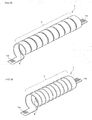
- FIG. 1 is schematic construction views of a flexible circuit board according to the present invention.
- FIG. 2 is views showing a method for production of a flexible circuit board according to the present invention.
- FIG. 3 is views showing a method for production of a flexible circuit board according to the present invention.
- FIG. 4 is schematic construction views of a flexible circuit board according to the present invention.
- FIG. 5 is views showing a method for production of a flexible circuit board according to the present invention.
- FIG. 6 is views showing a method for an expansion and contraction test of a flexible circuit board according to the present invention.
- FIG. 1( a ), FIG. 1( b ) and FIG. 4( a ) show the schematic constructions of the flexible circuit board according to this embodiment, respectively.
- the flexible circuit board 1 has an insulating film 2 made of a thermoplastic resin, a wiring layer 3 A which is formed on the insulating film 2 , and an insulating layer 4 which is formed on the wiring layer 3 A and which is made of a thermoplastic resin.
- the wiring layer 3 A is adhered on the insulating film 2 by means of an adhesive layer 8 , but other constructions may be possible in which the wiring layer 3 A is formed directly on the insulating film 2 without the provision of the adhesive layer 8 .
- the flexible circuit board 1 is provided, on at least a portion thereof, with a spiral part 5 which is shaped into a spiral shape, so that it is constructed to be expandable and contractable, and/or torsionally deformable in the spiral part 5 .
- a reference numeral 6 shown in FIG. 1( a ) denotes a hollow interior portion of the spiral part 5
- a reference character 1 A denotes terminals (which can be electrically connected to the wiring layer 3 A) arranged at opposite ends of the flexible circuit board 1 .
- the spiral part 5 of the flexible circuit board 1 may be formed in such a mariner that a part of its circumferential surface and another adjacent part of the circumferential surface (i.e., a part of an outer peripheral surface of one of adjacent spirals and a part of an inner peripheral surface of the other thereof) may mutually overlap with each other. According to this, it becomes possible to further improve the elasticity (expansion and contraction property) of the spiral part 5 , while further reducing the size of the flexible circuit board 1 .
- the wiring layer 3 A is formed by bonding a well-known metal foil, such as a rolled copper foil, an electrolytic copper foil, or the like, to the insulating film 2 by means of the adhesive layer 8 .
- the wiring layer 3 A can also be formed on a surface of the insulating film 2 (or a surface of the adhesive layer 8 formed on the insulating film 2 ) by means of an appropriate method such as vapor deposition, sputtering, or the like, by using a metal such as copper or silver.
- the adhesive layer 8 is formed by using a well-known thermoplastic resin such as polyimide, or a well-known thermosetting resin such as cyanate ester based resin, polyphenylene ether based resin, phenol based resin, naphthalene resin, urea resin, amino resin, alkyd resin, silicon resin, furan resin, unsaturated polyester resin, epoxy resin, polyurethane resin, etc.
- a well-known thermoplastic resin such as polyimide
- a well-known thermosetting resin such as cyanate ester based resin, polyphenylene ether based resin, phenol based resin, naphthalene resin, urea resin, amino resin, alkyd resin, silicon resin, furan resin, unsaturated polyester resin, epoxy resin, polyurethane resin, etc.
- the adhesive layer 8 can also be formed of any of the above-mentioned organic resins with an inorganic filler such as silica, alumina or the like dispersed therein.
- thermoplastic resins for the insulating film 2 and the insulating layer 4 , there are recommended thermoplastic resins in particular in cases where heat resistance is required, and the following are preferred: liquid crystal polymer (e.g., trade name “RODRUN” made by Unitika, Ltd., “EPE” made by Mitsubishi Chemical Corporation, “IDEMITSU LCP” made by an Idemitsu Petrochemical Company, Ltd., “Ekonol” made by Sumitomo Chemical Co., Ltd.
- liquid crystal polymer e.g., trade name “RODRUN” made by Unitika, Ltd., “EPE” made by Mitsubishi Chemical Corporation, “IDEMITSU LCP” made by an Idemitsu Petrochemical Company, Ltd., “Ekonol” made by Sumitomo Chemical Co., Ltd.
- polyamide imides e.g., polyamide imide obtained from trimellitic acid and aromatic diamines such as diaminodiphenylmethane, diaminodiphenyl ether, m-, or p-phenylenediamine, etc.
- thermoplastic polyimide e.g., trade name “AURUM”, made by Mitsui Chemicals, Inc.
- thermoplastic resins may be used.
- PEN polyethylenenaphthalate
- PET polyethylene terephthalate
- COP cycloolefin polymer
- the thermoplastic resins used for the insulating film 2 and the insulating layer 4 may be the same material, or different materials may be selected for them, respectively.
- a liquid crystal polymer is used for the insulating film 2 and the insulating layer 4 .
- the flexible circuit board 1 is formed, in at least a part thereof, with the spiral part 5 having the hollow interior portion 6 . Because of such a shape, it becomes possible for the flexible circuit board 1 to carry out elastic deformation, and when an external force acts on the flexible circuit board 1 , the flexible circuit board 1 as a whole can be deformed in an elastic (expandable and contractable) manner, thereby making it possible to prevent stress from concentrating locally thereon.
- the spiral part 5 is a part “shaped into a spiral shape”. That is, the flexible circuit board 1 is shaped in such a manner that it is able to maintain the spiral shape thereof by itself, without requiring any external support means, any auxiliary means, etc. Therefore, it is not necessary to provide a support rod separately, as in a conventional cable.
- the insulating film 2 and the insulating layer 4 are formed of the thermoplastic resin, so the flexible circuit board 1 , which has become unnecessary, can be restored to its original shape by being heating again, which leads to recycling or reuse of resources.
- the arrangement of the wiring layer 3 A is not limited to this, but may be such that wiring layers 3 A, 3 B are arranged on opposite sides, respectively, of the insulating film 2 , as shown in FIG. 4( b ).
- the wiring layer 3 A formed on one side surface be used as a signal line for signal transmission, whereas the wiring layer 3 B formed on the other side surface be used as a power line for supplying electric power.
- the thickness of a wiring layer used for the power line 3 B can be made thin in such a case. As a result, it is possible to further reduce the weight and size of the flexible circuit board 1 , and to improve the elasticity and flexibility thereof as well.
- FIG. 4( c ) it may be constructed such that wiring layers 3 A, 3 B formed on one side surface are used as a signal line for signal transmission and a power line for supplying electric power, respectively, whereas a wiring layer 3 C formed on the other side surface is used as a ground pattern, and at the same time, in the spiral part 5 , the ground pattern is arranged at an outer peripheral side than the signal line and the power line. That is, in FIG. 4( c ), an upper side is an outer peripheral side in the spiral part 5 , and a lower side is an inner peripheral side in the spiral part 5 .
- the ground pattern is arranged at the outer peripheral side, and hence, the ground pattern functions as a shield layer, thus making it possible to prevent the propagation of noise from the outside to the signal line and the power line which are arranged at the inner peripheral side. That is, higher connection reliability can be obtained.
- a metal-covered film 9 is prepared, as shown in metal-covered film 9 can be formed by forming the adhesive layer 8 on a surface of the insulating film 2 made of a thermoplastic resin, laminating a metal foil 30 on a surface of the adhesive layer 8 , and integrating these three layers with one another by means of thermocompression bonding.
- a technique of coating a varnish, which is a precursor of an insulating film, on a metal foil, and drying this precursor a technique of forming a metal layer on an insulating film by vapor deposition or sputtering, a technique of forming a wiring layer on an insulating film, which is coated with a conductive paste, by means of electrolysis plating, and so on.
- the wiring layer 3 A is formed, whereby the flexible circuit board 1 is obtained.
- the insulating layer 4 is obtained by coating a thermoplastic resin on the wiring layer 3 A.
- the insulating layer 4 may be formed by bonding the insulating film made of a thermoplastic resin by means of thermo compression.
- the single-sided flexible circuit board 1 having the insulating layer 4 can be obtained according to the steps shown in FIG. 3( a ) through 3 ( c ) which are described herein.
- the flexible circuit board 1 according to this embodiment can adopt not only the above-mentioned single sided structure but also a multilayer structure which is shown in the following. Reference will be made to a method for production of a multilayer flexible circuit board having a three-layer structure, while referring to FIG. 5( a ) through FIG. 5( c ).
- a metal-covered film 9 a single-sided flexible circuit board 1 and a metal foil 10 are prepared, and in addition, two adhesive sheets 11 for adhering these three sheets are prepared.
- the adhesive sheets 11 there is used the thermoplastic resin for the above-mentioned insulating layer 4 which has been formed into the shape of a sheet. These are laminated in a manner as illustrated, and then, those which are thus laminated are thermally compressed so that the three sheets are integrated with one another.
- a through hole 12 is formed at a desired position by the use of a drill or laser, and is then subjected to through hole plating 12 a , so that the individual layers including the metal foil 30 of the metal-covered film 9 , the wiring layer 3 A and the metal foil 10 are electrically connected to one another.
- a state in which wiring layers are electrically connected to one another through the plating is shown in FIG. 5( b ).
- it is also possible to electrically connect between the individual layers by filling an electrically conductive paste into the through hole 12 , and allowing the conductive paste to solidify.
- the metal foils 30 , 10 disposed on the opposite respective surfaces are formed into the wiring layers 3 A which have desired wiring patterns, respectively, by means of an appropriate technique such as etching, etc.
- insulating layers 4 are formed on the opposite surfaces, as in the above-mentioned technique (refer to FIG. 3( c )).
- the multilayer flexible circuit board 1 having a three-layer structure can be produced. Note that a form having the three-layer structure has been described here, but the structure of the multilayer flexible circuit board 1 is not limited to such a three-layer structure.
- the spiral part 5 is formed, after the flexible circuit board 1 has been produced according to the above-mentioned production method, by performing predetermined shaping processing with respect to the flexible circuit board 1 thus produced.
- the flexible circuit board 1 As shown in FIG. 2( b ), the flexible circuit board 1 according to this embodiment is formed with an arc shaped portion 1 B in a state before the shaping or forming of the spiral part 5 , and the spiral part 5 is formed by carrying out the shaping processing with respect to this arc shaped portion 1 B, which will be described below.
- the spiral part 5 As shown in FIG. 2( b ), almost the whole of the flexible circuit board 1 is formed in an arc shape only at leas a portion of the flexible circuit board 1 corresponding to the spiral part 5 should be formed in an arc shape.
- the spiral part 5 By forming the spiral part 5 with the arc shaped portion 1 B in this manner, the diameter of the hollow interior portion 6 of the spiral part 5 can be made almost constant. As a result, in cases where another wiring, etc. made to pass through the hollow interior portion 6 of the spiral part 5 , for example, the possibility that the wiring and the spiral part 5 interfere with each other can be reduced.
- the shaping processing of the spiral part 5 includes: a first step to wind the flexible circuit board 1 around a shaping device 13 of a circular column shape in a state in which tension is applied to the opposite ends of the flexible circuit board 1 , thereby to shape the spiral part 5 ; and a second step to heat a portion of the flexible circuit board 1 wound around the shaping device 13 , thereby to form the spiral part 5 in the flexible circuit board 1 .
- the flexible circuit board 1 is wound around the shaping device 13 , with tension being applied to the opposite ends of the flexible circuit board 1 , whereby a portion of the flexible circuit board 1 is shaped into a spiral shape.
- the size or length in the diametrical direction of the hollow interior portion 6 can be changed by changing the diameter of the shaping device 13 , and similarly, the number of turns of the spiral part 5 , the interval of adjacent turns of the spiral part 5 , and so on, can be set optionally or at will by changing the number of turns and the interval of adjacent turns of the shaping device 13 in a suitable manner.
- a tensile force at the time of applying tension to the flexible circuit board 1 should just be an applied force by which the spiral part 5 is at least formed or shaped in the flexible circuit board 1 in a reliable manner, and the applied force can be changed in a suitable manner in accordance with the thickness, the material, etc., of the flexible circuit board 1 .
- the flexible circuit board 1 which is formed into the spiral shape by applying tension to the opposite ends thereof, in particular at least the portion thereof formed into the spiral shape (that portion which is wound around the shaping device 13 ) is heated.
- the flexible circuit board 1 armed in the spiral shape is heated by putting the flexible circuit board 1 into a heating device together with the shaping device 13
- it may be constructed such that a heating member is arranged in the interior of the shaping device 13 , whereby at least that portion of the flexible circuit board 1 which is formed into the spiral shape is heated by the heat generated from the shaping device 13 .
- the temperature of heating is set to a temperature at which the surface temperature of the flexible circuit board 1 becomes equal to or higher than 150 degrees C. and less than a thermal deformation starting temperature of the liquid crystal polymer, and the time of heating is set within 1 hour.
- the heating is carried out at the temperature at which the surface temperature of the flexible circuit board 1 is equal to or higher than 150 degrees C. and less than the thermal deformation starting temperature of the liquid crystal polymer, the liquid crystal polymer is not fluidized to flow, and the external appearance and performance of the flexible circuit board 1 are not impaired.
- the heating temperature is such that the surface temperature of the flexible circuit board 1 becomes equal to or higher than 150 degrees C.
- the spiral part 5 can be formed or shaped with respect to the liquid crystal polymer in a reliable manner, and further, even after the heating is finished, the spiral part 5 does not return to its original shape.
- the heating time is within 1 hour, the efficiency of production can be improved, and at the same time, it becomes possible to avoid problems of the discoloration and thermal deformation of the liquid crystal polymer, as well as damage to the wiring layer 3 A, which would otherwise be generated by heating for an extended period of time.
- the spiral part 5 can be shaped or formed by changing the above-mentioned heating temperature and heating time in a suitable manner (however, an upper limit of the heating temperature is a temperature which becomes less than the thermal deformation starting temperature of the material thus selected).
- the flexible circuit board 1 which is formed with the spiral part 5 and which can be deformed in an elastic manner and/or in a torsional manner.
- the first step and the second step may be carried out at the same time.
- Esperflex (trade name) (made of Sumitomo Metal Mining, Co., Ltd., polyimide film: Kapton-EN, film thickness: 50 ⁇ m, thickness of copper foil: 18 ⁇ m) which is a single-sided copper-covered two-layer polyimide film.
- Esperflex trade name
- a copper-covered film there was prepared a single-sided copper-covered three-layer polyimide film (polyimide film: Kapton-EN, film thickness: 50 ⁇ m, thickness of rolled copper foil: 18 ⁇ m, adhesive: epoxy resin, thickness of adhesive layer: 10 ⁇ m).
- etching processing was carried out on these samples, so that a wiring layer 3 A having a wiring pattern as shown in FIG. 6( a ) was formed, and a single-sided flexible circuit board 1 was obtained.
- the width of the circuit board, the width of wiring, and so on, are as shown in this figure.
- the polyimide film, Kapton-EN, used herein has a thermosetting property, and the circuit boards of the first through tenth comparative examples and the flexible circuit board 1 according to this embodiment are different from each other at least in this point.
- the single-sided flexible circuit board was shaped into the circular spiral part 5 under the conditions (surface temperature (degrees C.) of the board, shaping time (h)) which are described in Table 1. Note that here, the same as the shaping device 13 used in this embodiment is used as a shaping device.
- FIG. 6( b ) schematically shows a device for carrying out the “repeated expansion and contraction test”.
- the opposite ends of each flexible circuit board 1 to be tested are fixedly secured at fastening portions 15 to a stationary or fixed plate 14 and a vertically movable plate 16 , respectively.
- the distance between the fixed plate 14 and the vertically movable plate 16 was set such that each flexible circuit board 1 was in the most contracted state thereof.
- the distance between the fixed plate 14 and the vertically movable plate 16 in a fully expanded state of each flexible circuit board 1 was set to be a value at which the flexible circuit board 1 become the most expanded.
- the vertically movable plate 16 was moved to reciprocate in the vertical direction, 100,000 times at a speed of 100 mm/second. Thereafter, those flexible circuit boards in which the resistance value of the wiring layer 3 A after the expansion and contraction thereof increased by 10% or more from that before the expansion and contraction were assumed to be “defective”.
- the number of tests (N) was set to 20 for each sample. The results of such tests are shown in Table 2.
- “success or failure in shape maintenance” in Table 2 is an evaluation on whether the size in the diametrical direction of the hollow interior portion 6 of each spiral part 5 was maintained with respect to the shape hereof after the tests.
- “success or failure in shaping” is an examination as to whether the size in the diametrical direction of the hollow interior portion 6 was a target value, after each flexible circuit board was taken out from the shaping device 13 .
- the criteria for the success or failure in shaping and the criteria for the success or failure in shape maintenance are defined as follows.
- the criteria for the external appearance are defined as follows. O: the outflow of the insulating film or the insulating layer is not recognized; and x: the outflow of the insulating film or the insulating layer is recognized.
- the liquid crystal polymer was used for the insulating film 2 and the insulating layer 4 , similar to this embodiment. That is, first, as a copper-covered film, there was prepared Esperflex L (trade name) (made by Nippon Steel Chemical Co., Ltd., film thickness: 50 ⁇ m, thickness of rolled copper foil: 18 ⁇ m, thermal deformation starting temperature: 290 degrees C.) which is a single-sided copper-covered liquid crystal polymer film. Subsequently, etching processing was carried out on these samples, so that a wiring layer 3 A having a wiring pattern as shown in FIG. 6( a ) was formed, and a single-sided flexible circuit board 1 was obtained.
- Esperflex L trade name
- etching processing was carried out on these samples, so that a wiring layer 3 A having a wiring pattern as shown in FIG. 6( a ) was formed, and a single-sided flexible circuit board 1 was obtained.
- the spiral part 5 can be shaped, and even after the above-mentioned tests have been carried out, the size in the diametrical direction of the hollow interior portion 6 is maintained, and in addition, the external appearance is also at an acceptable level.
- the temperature of “150 degrees C.” is a lower limit heating temperature at which the spiral part 5 can be formed and the size in the diametrical direction of the hollow interior portion 6 thus formed can be maintained even if the expansion and contraction tests are carried out (although the liquid crystal polymer is used in this embodiment, this temperature can also be of course changed in cases where other materials are used).
- the heating time is here set to 1 hour, but according to inventors' keen study and examination, it has been found that even if the heating time is less than 1 hour, “the success in shaping”, “the success in shape maintenance”, and “the external appearance” each sufficiently reach an acceptable level.
- the spiral part 5 can not be formed, or the size in the diametrical direction of the hollow interior portion 6 can not be maintained.
- the spiral part 5 can be shaped or formed when the heating temperature is a temperature at which the surface temperature of the flexible circuit board becomes equal to or higher than 150 degrees C. and less than the thermal deformation starting temperature of the liquid crystal polymer, and when the shaping time is within 1 hour, and even if the above-mentioned expansion and contraction tests are carried out, the size in the diametrical direction of the hollow interior portion 6 can be maintained.
- the external appearance is also at an acceptable level.
- the present invention it becomes possible to provide a flexible circuit board and a method for production thereof in which in cases where elastic wiring in movable parts of a robot, etc., is required, the wiring can be made to expand and contract with a simple arrangement, and at the same time, the circuit board is excellent in weight reduction as well as size reduction, and breaking or disconnection and exfoliation of a wiring layer do not take place easily, even in cases where the circuit board is deformed in a repeated manner.
Landscapes
- Engineering & Computer Science (AREA)
- Microelectronics & Electronic Packaging (AREA)
- Structure Of Printed Boards (AREA)
- Insulated Conductors (AREA)
- Manufacturing Of Printed Wiring (AREA)
Applications Claiming Priority (3)
| Application Number | Priority Date | Filing Date | Title |
|---|---|---|---|
| JP2010095804A JP5284308B2 (ja) | 2010-04-19 | 2010-04-19 | フレキシブル回路基板及びその製造方法 |
| JP2010-095804 | 2010-04-19 | ||
| PCT/JP2010/073386 WO2011132343A1 (ja) | 2010-04-19 | 2010-12-24 | フレキシブル回路基板及びその製造方法 |
Publications (2)
| Publication Number | Publication Date |
|---|---|
| US20130056248A1 US20130056248A1 (en) | 2013-03-07 |
| US9155193B2 true US9155193B2 (en) | 2015-10-06 |
Family
ID=44833890
Family Applications (1)
| Application Number | Title | Priority Date | Filing Date |
|---|---|---|---|
| US13/641,769 Active 2031-10-02 US9155193B2 (en) | 2010-04-19 | 2010-12-24 | Flexible circuit board and its method for production |
Country Status (6)
| Country | Link |
|---|---|
| US (1) | US9155193B2 (de) |
| EP (1) | EP2563101B1 (de) |
| JP (1) | JP5284308B2 (de) |
| CN (1) | CN102870504B (de) |
| TW (1) | TWI514935B (de) |
| WO (1) | WO2011132343A1 (de) |
Cited By (1)
| Publication number | Priority date | Publication date | Assignee | Title |
|---|---|---|---|---|
| US10760892B2 (en) | 2017-03-30 | 2020-09-01 | Seiko Epson Corporation | Sensor |
Families Citing this family (29)
| Publication number | Priority date | Publication date | Assignee | Title |
|---|---|---|---|---|
| JP2013218996A (ja) * | 2012-04-06 | 2013-10-24 | Okuda Ichiyoshi | ケーブルの外線をスパイラル状に巻き込む構造 |
| US9226402B2 (en) * | 2012-06-11 | 2015-12-29 | Mc10, Inc. | Strain isolation structures for stretchable electronics |
| US9101175B2 (en) * | 2012-06-28 | 2015-08-11 | Revision Military S.A.R.L. | Helmet configured for electronics |
| WO2014046014A1 (ja) * | 2012-09-20 | 2014-03-27 | 株式会社クラレ | 回路基板およびその製造方法 |
| US9353932B2 (en) | 2013-03-13 | 2016-05-31 | Palo Alto Research Center Incorporated | LED light bulb with structural support |
| US9528689B2 (en) | 2013-03-13 | 2016-12-27 | Palo Alto Research Center Incorporated | LED lighting device with cured structural support |
| TWI573498B (zh) * | 2013-07-26 | 2017-03-01 | Adv Flexible Circuits Co Ltd | The flattened cladding structure of soft circuit board |
| TWI622328B (zh) * | 2014-03-03 | 2018-04-21 | Stretchable flexible circuit board | |
| MX337677B (es) * | 2014-03-10 | 2016-03-10 | Paulino Vacas Jacques | Tarjeta madre textil con diseño modular e intercambiable para monitoreo, informacion y control. |
| TWI573503B (zh) * | 2014-06-09 | 2017-03-01 | The Power Supply Path Structure of Soft Circuit Board | |
| JP6578646B2 (ja) | 2014-10-24 | 2019-09-25 | セイコーエプソン株式会社 | ロボット |
| JP2016083716A (ja) * | 2014-10-24 | 2016-05-19 | セイコーエプソン株式会社 | ロボット |
| WO2016132868A1 (ja) * | 2015-02-17 | 2016-08-25 | Nok株式会社 | 触覚センサの被覆構造及び触覚センサ |
| JP2017020631A (ja) * | 2015-07-15 | 2017-01-26 | アズビル株式会社 | ポジショナ |
| WO2017084014A1 (zh) * | 2015-11-16 | 2017-05-26 | 深圳市洛书和科技发展有限公司 | 可挠性导电连接件及模块化电子电路 |
| EP3208890A1 (de) * | 2016-02-19 | 2017-08-23 | Thomson Licensing | Steckdose für elektrischen stecker und flexibler elektrischer stecker |
| CN108012406A (zh) * | 2017-12-06 | 2018-05-08 | 广州兴森快捷电路科技有限公司 | 可拉伸的fpc板及其制作方法 |
| CN108650780B (zh) * | 2018-05-23 | 2019-07-16 | 深圳市爱升精密电路科技有限公司 | 一种柔性印刷电路板 |
| CN108495488B (zh) * | 2018-05-23 | 2019-06-21 | 深圳市汇芯线路科技有限公司 | 一种多层印刷线路板的制作方法 |
| CN109195312B (zh) * | 2018-09-14 | 2024-04-09 | 江西合力泰科技有限公司 | 补强板及提高补强板蚀刻精度的方法 |
| CN109640513B (zh) * | 2019-01-22 | 2024-04-02 | 广州安费诺诚信软性电路有限公司 | 一种自弹性轴向伸缩软性电路板及其制备方法 |
| JP6887475B2 (ja) * | 2019-05-24 | 2021-06-16 | Nissha株式会社 | 筒状プリント基板およびプリント基板一体成形品 |
| JP7227281B2 (ja) | 2021-01-06 | 2023-02-21 | 矢崎総業株式会社 | フレキシブル配索材 |
| CN113593775B (zh) * | 2021-07-30 | 2023-04-14 | 长春捷翼汽车科技股份有限公司 | 一种制造线束的方法及线束 |
| JP7772093B2 (ja) * | 2021-12-27 | 2025-11-18 | 株式会社オートネットワーク技術研究所 | 扁平カールコード |
| CN114286503B (zh) * | 2021-12-28 | 2024-02-09 | 武汉天马微电子有限公司 | 柔性电路板及其制备方法、显示模组 |
| KR20230130203A (ko) * | 2022-03-02 | 2023-09-12 | 삼성디스플레이 주식회사 | 표시 장치 |
| US20240392863A1 (en) * | 2023-05-24 | 2024-11-28 | Jtekt Bearings North America Llc | Actuator having wiring pathway arrangement |
| EP4561270A1 (de) * | 2023-11-21 | 2025-05-28 | Cisel S.r.l. - Circuiti Stampati Per Applicazioni Elettroniche | Flexible leiterplatte |
Citations (18)
| Publication number | Priority date | Publication date | Assignee | Title |
|---|---|---|---|---|
| US3300572A (en) * | 1963-12-18 | 1967-01-24 | Sanders Associates Inc | Extensible and retractable flexible circuit cable |
| US4861945A (en) | 1988-12-09 | 1989-08-29 | Precision Interconnect Corporation | Yieldably extensible self-retracting shielded cable |
| JPH0857792A (ja) | 1994-08-18 | 1996-03-05 | Meikikou:Kk | 水平多関節ロボットにおけるケーブルの処理方法 |
| US5525760A (en) * | 1993-03-30 | 1996-06-11 | The United States Of America As Represented By The United States Department Of Energy | Fan-fold shielded electrical leads |
| US5631446A (en) * | 1995-06-07 | 1997-05-20 | Hughes Electronics | Microstrip flexible printed wiring board interconnect line |
| US5747743A (en) * | 1994-02-04 | 1998-05-05 | Nippondenso Co., Ltd. | Coil-shaped flexible printed circuit board |
| JP2002094191A (ja) | 2000-09-18 | 2002-03-29 | Matsushita Electric Ind Co Ltd | フレキシブル基板およびこれを用いた装置 |
| US20030094697A1 (en) | 2001-11-21 | 2003-05-22 | Takaaki Higashida | Circuit substrate and its manufacturing method |
| JP2006093562A (ja) | 2004-09-27 | 2006-04-06 | Fujikura Ltd | フレキシブルプリント基板およびその設置構造 |
| CN1829412A (zh) | 2005-02-17 | 2006-09-06 | 新日铁化学株式会社 | 可反复弯曲的双面挠性电路基板 |
| US7400513B2 (en) * | 2003-04-22 | 2008-07-15 | Nihon Dempa Kogyo Co., Ltd. | Conductive printed board, multicore cable and ultrasonic probe using the same |
| US20080182435A1 (en) | 2007-01-31 | 2008-07-31 | Nitto Denko Corporation | Connecting configuration for flexible wired circuit board and electronic device |
| US7531752B2 (en) * | 2003-07-24 | 2009-05-12 | Nec Corporation | Flexible substrate and electronic device |
| JP2009246380A (ja) | 2009-07-14 | 2009-10-22 | Fujitsu Ltd | 携帯機器 |
| US20100170692A1 (en) * | 2009-01-06 | 2010-07-08 | Hsin-I Lu | Spiral electrical connection device and slide-type electronic device |
| US7796883B2 (en) * | 2007-04-09 | 2010-09-14 | Microsoft Corporation | Flexible circuit connection |
| US8227699B2 (en) * | 2007-01-26 | 2012-07-24 | Nitto Denko Corporation | Printed circuit board |
| US8397378B2 (en) * | 2008-04-14 | 2013-03-19 | Samsung Electro-Mechanics Co., Ltd. | Manufacturing an insulating sheet, a copper clad laminate, and a printed circuit board |
Family Cites Families (2)
| Publication number | Priority date | Publication date | Assignee | Title |
|---|---|---|---|---|
| JP2003046275A (ja) * | 2001-07-31 | 2003-02-14 | Fujitsu Ltd | 携帯機器 |
| CN100574556C (zh) * | 2004-08-02 | 2009-12-23 | 松下电器产业株式会社 | 柔性印刷基板 |
-
2010
- 2010-04-19 JP JP2010095804A patent/JP5284308B2/ja active Active
- 2010-12-24 US US13/641,769 patent/US9155193B2/en active Active
- 2010-12-24 EP EP10850284.0A patent/EP2563101B1/de active Active
- 2010-12-24 CN CN201080066280.6A patent/CN102870504B/zh active Active
- 2010-12-24 WO PCT/JP2010/073386 patent/WO2011132343A1/ja not_active Ceased
-
2011
- 2011-04-18 TW TW100113368A patent/TWI514935B/zh active
Patent Citations (22)
| Publication number | Priority date | Publication date | Assignee | Title |
|---|---|---|---|---|
| US3300572A (en) * | 1963-12-18 | 1967-01-24 | Sanders Associates Inc | Extensible and retractable flexible circuit cable |
| US4861945A (en) | 1988-12-09 | 1989-08-29 | Precision Interconnect Corporation | Yieldably extensible self-retracting shielded cable |
| US5525760A (en) * | 1993-03-30 | 1996-06-11 | The United States Of America As Represented By The United States Department Of Energy | Fan-fold shielded electrical leads |
| US5747743A (en) * | 1994-02-04 | 1998-05-05 | Nippondenso Co., Ltd. | Coil-shaped flexible printed circuit board |
| JPH0857792A (ja) | 1994-08-18 | 1996-03-05 | Meikikou:Kk | 水平多関節ロボットにおけるケーブルの処理方法 |
| US5631446A (en) * | 1995-06-07 | 1997-05-20 | Hughes Electronics | Microstrip flexible printed wiring board interconnect line |
| JP2002094191A (ja) | 2000-09-18 | 2002-03-29 | Matsushita Electric Ind Co Ltd | フレキシブル基板およびこれを用いた装置 |
| US20030094697A1 (en) | 2001-11-21 | 2003-05-22 | Takaaki Higashida | Circuit substrate and its manufacturing method |
| CN1420714A (zh) | 2001-11-21 | 2003-05-28 | 松下电器产业株式会社 | 薄型电路板及薄型电路板的制造方法 |
| US7400513B2 (en) * | 2003-04-22 | 2008-07-15 | Nihon Dempa Kogyo Co., Ltd. | Conductive printed board, multicore cable and ultrasonic probe using the same |
| US7531752B2 (en) * | 2003-07-24 | 2009-05-12 | Nec Corporation | Flexible substrate and electronic device |
| JP2006093562A (ja) | 2004-09-27 | 2006-04-06 | Fujikura Ltd | フレキシブルプリント基板およびその設置構造 |
| CN1829412A (zh) | 2005-02-17 | 2006-09-06 | 新日铁化学株式会社 | 可反复弯曲的双面挠性电路基板 |
| US8227699B2 (en) * | 2007-01-26 | 2012-07-24 | Nitto Denko Corporation | Printed circuit board |
| US20080182435A1 (en) | 2007-01-31 | 2008-07-31 | Nitto Denko Corporation | Connecting configuration for flexible wired circuit board and electronic device |
| CN101237743A (zh) | 2007-01-31 | 2008-08-06 | 日东电工株式会社 | 柔性布线电路基板的连接结构以及电子设备 |
| JP2008187154A (ja) | 2007-01-31 | 2008-08-14 | Nitto Denko Corp | フレキシブル配線回路基板の接続構造および電子機器 |
| US7641488B2 (en) * | 2007-01-31 | 2010-01-05 | Nitto Denko Corporation | Connecting configuration for flexible wired circuit board and electronic device |
| US7796883B2 (en) * | 2007-04-09 | 2010-09-14 | Microsoft Corporation | Flexible circuit connection |
| US8397378B2 (en) * | 2008-04-14 | 2013-03-19 | Samsung Electro-Mechanics Co., Ltd. | Manufacturing an insulating sheet, a copper clad laminate, and a printed circuit board |
| US20100170692A1 (en) * | 2009-01-06 | 2010-07-08 | Hsin-I Lu | Spiral electrical connection device and slide-type electronic device |
| JP2009246380A (ja) | 2009-07-14 | 2009-10-22 | Fujitsu Ltd | 携帯機器 |
Non-Patent Citations (4)
| Title |
|---|
| Chinese Office Action (With English Translation), Chinese Application No. 201080066280.6, dated Dec. 22, 2014 (13 pages). |
| European Search Report, European Patent Application No. 10850284.0, dated Aug. 9, 2013 (9 pages). |
| International Search Report dated Feb. 8, 2011. |
| Taiwanese Office Action, dated Dec. 26, 2014 (6 pages). |
Cited By (1)
| Publication number | Priority date | Publication date | Assignee | Title |
|---|---|---|---|---|
| US10760892B2 (en) | 2017-03-30 | 2020-09-01 | Seiko Epson Corporation | Sensor |
Also Published As
| Publication number | Publication date |
|---|---|
| EP2563101B1 (de) | 2018-03-14 |
| WO2011132343A1 (ja) | 2011-10-27 |
| EP2563101A4 (de) | 2013-09-11 |
| HK1175927A1 (zh) | 2013-07-12 |
| EP2563101A1 (de) | 2013-02-27 |
| TWI514935B (zh) | 2015-12-21 |
| JP2011228077A (ja) | 2011-11-10 |
| CN102870504B (zh) | 2016-01-20 |
| TW201201637A (en) | 2012-01-01 |
| CN102870504A (zh) | 2013-01-09 |
| JP5284308B2 (ja) | 2013-09-11 |
| US20130056248A1 (en) | 2013-03-07 |
Similar Documents
| Publication | Publication Date | Title |
|---|---|---|
| US9155193B2 (en) | Flexible circuit board and its method for production | |
| JP6029262B2 (ja) | フレキシブル回路体 | |
| JP5600030B2 (ja) | フレキシブル回路基板 | |
| US9024198B2 (en) | Flexible circuit board and method for production thereof | |
| KR100374960B1 (ko) | 플렉시블 배선판 및 이를 이용한 전자 기기 | |
| US9743532B2 (en) | Flexible printed circuit board and manufacturing method of flexible printed circuit board | |
| JP2016134438A (ja) | フレキシブルプリント基板およびフレキシブルプリント基板の製造方法 | |
| JP2015228533A (ja) | フレキシブル回路体の製造方法 | |
| JP5151025B2 (ja) | フレキシブル回路基板 | |
| EP3544392B1 (de) | Elektronische vorrichtung und verfahren zur herstellung davon | |
| JP2010040934A (ja) | リジッドフレックス回路板 | |
| HK1175927B (en) | Flexible circuit board and production method therefor | |
| CN109548277A (zh) | 一种耐折弯柔性线路软板及其制备方法 | |
| WO2018199084A1 (ja) | 配線基板およびその製造方法 | |
| EP2988577A1 (de) | Leiterplatte | |
| JP4907328B2 (ja) | プリント配線基板、その製造方法および電子機器 | |
| JP2002231057A (ja) | シールドハーネス及び該シールドハーネスの製造方法 | |
| KR20130034787A (ko) | 카메라 모듈 | |
| JP2012109406A (ja) | フレキシブル多層回路基板の製造方法 | |
| KR102016612B1 (ko) | 기판 적층 구조물과 이의 제조방법 | |
| JP3101047U (ja) | 多層フレキシブルプリント配線板 | |
| WO2023238562A1 (ja) | 多層基板 | |
| JP2008226512A (ja) | フラットケーブル及びその製造方法 |
Legal Events
| Date | Code | Title | Description |
|---|---|---|---|
| AS | Assignment |
Owner name: NIPPON MEKTRON, LTD., JAPAN Free format text: ASSIGNMENT OF ASSIGNORS INTEREST;ASSIGNORS:KAJIYA, ATSUSHI;YOSHIHARA, HIDEKAZU;REEL/FRAME:029300/0864 Effective date: 20121102 |
|
| STCF | Information on status: patent grant |
Free format text: PATENTED CASE |
|
| MAFP | Maintenance fee payment |
Free format text: PAYMENT OF MAINTENANCE FEE, 4TH YEAR, LARGE ENTITY (ORIGINAL EVENT CODE: M1551); ENTITY STATUS OF PATENT OWNER: LARGE ENTITY Year of fee payment: 4 |
|
| MAFP | Maintenance fee payment |
Free format text: PAYMENT OF MAINTENANCE FEE, 8TH YEAR, LARGE ENTITY (ORIGINAL EVENT CODE: M1552); ENTITY STATUS OF PATENT OWNER: LARGE ENTITY Year of fee payment: 8 |
|
| AS | Assignment |
Owner name: MEKTEC CORPORATION, JAPAN Free format text: CHANGE OF NAME;ASSIGNOR:NIPPON MEKTRON, LTD.;REEL/FRAME:072961/0045 Effective date: 20240701 |