WO1994015366A1 - Dispositif a semiconducteurs - Google Patents
Dispositif a semiconducteurs Download PDFInfo
- Publication number
- WO1994015366A1 WO1994015366A1 PCT/JP1993/001850 JP9301850W WO9415366A1 WO 1994015366 A1 WO1994015366 A1 WO 1994015366A1 JP 9301850 W JP9301850 W JP 9301850W WO 9415366 A1 WO9415366 A1 WO 9415366A1
- Authority
- WO
- WIPO (PCT)
- Prior art keywords
- insulating film
- semiconductor device
- region
- source
- semiconductor
- Prior art date
- Legal status (The legal status is an assumption and is not a legal conclusion. Google has not performed a legal analysis and makes no representation as to the accuracy of the status listed.)
- Ceased
Links
Classifications
-
- H—ELECTRICITY
- H10—SEMICONDUCTOR DEVICES; ELECTRIC SOLID-STATE DEVICES NOT OTHERWISE PROVIDED FOR
- H10D—INORGANIC ELECTRIC SEMICONDUCTOR DEVICES
- H10D64/00—Electrodes of devices having potential barriers
- H10D64/60—Electrodes characterised by their materials
- H10D64/66—Electrodes having a conductor capacitively coupled to a semiconductor by an insulator, e.g. MIS electrodes
- H10D64/68—Electrodes having a conductor capacitively coupled to a semiconductor by an insulator, e.g. MIS electrodes characterised by the insulator, e.g. by the gate insulator
- H10D64/681—Electrodes having a conductor capacitively coupled to a semiconductor by an insulator, e.g. MIS electrodes characterised by the insulator, e.g. by the gate insulator having a compositional variation, e.g. multilayered
- H10D64/685—Electrodes having a conductor capacitively coupled to a semiconductor by an insulator, e.g. MIS electrodes characterised by the insulator, e.g. by the gate insulator having a compositional variation, e.g. multilayered being perpendicular to the channel plane
-
- H—ELECTRICITY
- H10—SEMICONDUCTOR DEVICES; ELECTRIC SOLID-STATE DEVICES NOT OTHERWISE PROVIDED FOR
- H10D—INORGANIC ELECTRIC SEMICONDUCTOR DEVICES
- H10D30/00—Field-effect transistors [FET]
- H10D30/01—Manufacture or treatment
- H10D30/021—Manufacture or treatment of FETs having insulated gates [IGFET]
- H10D30/031—Manufacture or treatment of FETs having insulated gates [IGFET] of thin-film transistors [TFT]
- H10D30/0321—Manufacture or treatment of FETs having insulated gates [IGFET] of thin-film transistors [TFT] comprising silicon, e.g. amorphous silicon or polysilicon
- H10D30/0323—Manufacture or treatment of FETs having insulated gates [IGFET] of thin-film transistors [TFT] comprising silicon, e.g. amorphous silicon or polysilicon comprising monocrystalline silicon
-
- H—ELECTRICITY
- H10—SEMICONDUCTOR DEVICES; ELECTRIC SOLID-STATE DEVICES NOT OTHERWISE PROVIDED FOR
- H10D—INORGANIC ELECTRIC SEMICONDUCTOR DEVICES
- H10D30/00—Field-effect transistors [FET]
- H10D30/60—Insulated-gate field-effect transistors [IGFET]
- H10D30/67—Thin-film transistors [TFT]
- H10D30/6704—Thin-film transistors [TFT] having supplementary regions or layers in the thin films or in the insulated bulk substrates for controlling properties of the device
- H10D30/6713—Thin-film transistors [TFT] having supplementary regions or layers in the thin films or in the insulated bulk substrates for controlling properties of the device characterised by the properties of the source or drain regions, e.g. compositions or sectional shapes
-
- H—ELECTRICITY
- H10—SEMICONDUCTOR DEVICES; ELECTRIC SOLID-STATE DEVICES NOT OTHERWISE PROVIDED FOR
- H10D—INORGANIC ELECTRIC SEMICONDUCTOR DEVICES
- H10D30/00—Field-effect transistors [FET]
- H10D30/60—Insulated-gate field-effect transistors [IGFET]
- H10D30/67—Thin-film transistors [TFT]
- H10D30/6704—Thin-film transistors [TFT] having supplementary regions or layers in the thin films or in the insulated bulk substrates for controlling properties of the device
- H10D30/6727—Thin-film transistors [TFT] having supplementary regions or layers in the thin films or in the insulated bulk substrates for controlling properties of the device having source or drain regions connected to bulk conducting substrates
-
- H—ELECTRICITY
- H10—SEMICONDUCTOR DEVICES; ELECTRIC SOLID-STATE DEVICES NOT OTHERWISE PROVIDED FOR
- H10D—INORGANIC ELECTRIC SEMICONDUCTOR DEVICES
- H10D30/00—Field-effect transistors [FET]
- H10D30/60—Insulated-gate field-effect transistors [IGFET]
- H10D30/67—Thin-film transistors [TFT]
- H10D30/6729—Thin-film transistors [TFT] characterised by the electrodes
- H10D30/6737—Thin-film transistors [TFT] characterised by the electrodes characterised by the electrode materials
- H10D30/6739—Conductor-insulator-semiconductor electrodes
-
- H—ELECTRICITY
- H10—SEMICONDUCTOR DEVICES; ELECTRIC SOLID-STATE DEVICES NOT OTHERWISE PROVIDED FOR
- H10D—INORGANIC ELECTRIC SEMICONDUCTOR DEVICES
- H10D64/00—Electrodes of devices having potential barriers
- H10D64/01—Manufacture or treatment
- H10D64/013—Manufacture or treatment of electrodes having a conductor capacitively coupled to a semiconductor by an insulator
- H10D64/01302—Manufacture or treatment of electrodes having a conductor capacitively coupled to a semiconductor by an insulator the insulator being formed after the semiconductor body, the semiconductor being silicon
- H10D64/01332—Making the insulator
- H10D64/0135—Making the insulator by deposition of a layer, e.g. metal, metal compound or polysilicon, followed by transformation thereof into the insulator
-
- H—ELECTRICITY
- H10—SEMICONDUCTOR DEVICES; ELECTRIC SOLID-STATE DEVICES NOT OTHERWISE PROVIDED FOR
- H10D—INORGANIC ELECTRIC SEMICONDUCTOR DEVICES
- H10D64/00—Electrodes of devices having potential barriers
- H10D64/60—Electrodes characterised by their materials
- H10D64/66—Electrodes having a conductor capacitively coupled to a semiconductor by an insulator, e.g. MIS electrodes
- H10D64/68—Electrodes having a conductor capacitively coupled to a semiconductor by an insulator, e.g. MIS electrodes characterised by the insulator, e.g. by the gate insulator
- H10D64/691—Electrodes having a conductor capacitively coupled to a semiconductor by an insulator, e.g. MIS electrodes characterised by the insulator, e.g. by the gate insulator comprising metallic compounds, e.g. metal oxides or metal silicates
-
- H—ELECTRICITY
- H10—SEMICONDUCTOR DEVICES; ELECTRIC SOLID-STATE DEVICES NOT OTHERWISE PROVIDED FOR
- H10D—INORGANIC ELECTRIC SEMICONDUCTOR DEVICES
- H10D84/00—Integrated devices formed in or on semiconductor substrates that comprise only semiconducting layers, e.g. on Si wafers or on GaAs-on-Si wafers
- H10D84/80—Integrated devices formed in or on semiconductor substrates that comprise only semiconducting layers, e.g. on Si wafers or on GaAs-on-Si wafers characterised by the integration of at least one component covered by groups H10D12/00 or H10D30/00, e.g. integration of IGFETs
- H10D84/82—Integrated devices formed in or on semiconductor substrates that comprise only semiconducting layers, e.g. on Si wafers or on GaAs-on-Si wafers characterised by the integration of at least one component covered by groups H10D12/00 or H10D30/00, e.g. integration of IGFETs of only field-effect components
- H10D84/83—Integrated devices formed in or on semiconductor substrates that comprise only semiconducting layers, e.g. on Si wafers or on GaAs-on-Si wafers characterised by the integration of at least one component covered by groups H10D12/00 or H10D30/00, e.g. integration of IGFETs of only field-effect components of only insulated-gate FETs [IGFET]
- H10D84/85—Complementary IGFETs, e.g. CMOS
-
- H—ELECTRICITY
- H10—SEMICONDUCTOR DEVICES; ELECTRIC SOLID-STATE DEVICES NOT OTHERWISE PROVIDED FOR
- H10D—INORGANIC ELECTRIC SEMICONDUCTOR DEVICES
- H10D86/00—Integrated devices formed in or on insulating or conducting substrates, e.g. formed in silicon-on-insulator [SOI] substrates or on stainless steel or glass substrates
- H10D86/201—Integrated devices formed in or on insulating or conducting substrates, e.g. formed in silicon-on-insulator [SOI] substrates or on stainless steel or glass substrates the substrates comprising an insulating layer on a semiconductor body, e.g. SOI
-
- H—ELECTRICITY
- H10—SEMICONDUCTOR DEVICES; ELECTRIC SOLID-STATE DEVICES NOT OTHERWISE PROVIDED FOR
- H10D—INORGANIC ELECTRIC SEMICONDUCTOR DEVICES
- H10D88/00—Three-dimensional [3D] integrated devices
-
- H—ELECTRICITY
- H10—SEMICONDUCTOR DEVICES; ELECTRIC SOLID-STATE DEVICES NOT OTHERWISE PROVIDED FOR
- H10W—GENERIC PACKAGES, INTERCONNECTIONS, CONNECTORS OR OTHER CONSTRUCTIONAL DETAILS OF DEVICES COVERED BY CLASS H10
- H10W70/00—Package substrates; Interposers; Redistribution layers [RDL]
- H10W70/60—Insulating or insulated package substrates; Interposers; Redistribution layers
- H10W70/67—Insulating or insulated package substrates; Interposers; Redistribution layers characterised by their insulating layers or insulating parts
- H10W70/68—Shapes or dispositions thereof
- H10W70/6875—Shapes or dispositions thereof being on a metallic substrate, e.g. insulated metal substrates [IMS]
-
- H—ELECTRICITY
- H10—SEMICONDUCTOR DEVICES; ELECTRIC SOLID-STATE DEVICES NOT OTHERWISE PROVIDED FOR
- H10P—GENERIC PROCESSES OR APPARATUS FOR THE MANUFACTURE OR TREATMENT OF DEVICES COVERED BY CLASS H10
- H10P14/00—Formation of materials, e.g. in the shape of layers or pillars
- H10P14/60—Formation of materials, e.g. in the shape of layers or pillars of insulating materials
- H10P14/63—Formation of materials, e.g. in the shape of layers or pillars of insulating materials characterised by the formation processes
- H10P14/6302—Non-deposition formation processes
- H10P14/6304—Formation by oxidation, e.g. oxidation of the substrate
- H10P14/6306—Formation by oxidation, e.g. oxidation of the substrate of the semiconductor materials
- H10P14/6308—Formation by oxidation, e.g. oxidation of the substrate of the semiconductor materials of Group IV semiconductors
- H10P14/6309—Formation by oxidation, e.g. oxidation of the substrate of the semiconductor materials of Group IV semiconductors of silicon in uncombined form, i.e. pure silicon
-
- H—ELECTRICITY
- H10—SEMICONDUCTOR DEVICES; ELECTRIC SOLID-STATE DEVICES NOT OTHERWISE PROVIDED FOR
- H10P—GENERIC PROCESSES OR APPARATUS FOR THE MANUFACTURE OR TREATMENT OF DEVICES COVERED BY CLASS H10
- H10P14/00—Formation of materials, e.g. in the shape of layers or pillars
- H10P14/60—Formation of materials, e.g. in the shape of layers or pillars of insulating materials
- H10P14/63—Formation of materials, e.g. in the shape of layers or pillars of insulating materials characterised by the formation processes
- H10P14/6302—Non-deposition formation processes
- H10P14/6304—Formation by oxidation, e.g. oxidation of the substrate
- H10P14/6314—Formation by oxidation, e.g. oxidation of the substrate of a metallic layer
-
- H—ELECTRICITY
- H10—SEMICONDUCTOR DEVICES; ELECTRIC SOLID-STATE DEVICES NOT OTHERWISE PROVIDED FOR
- H10P—GENERIC PROCESSES OR APPARATUS FOR THE MANUFACTURE OR TREATMENT OF DEVICES COVERED BY CLASS H10
- H10P14/00—Formation of materials, e.g. in the shape of layers or pillars
- H10P14/60—Formation of materials, e.g. in the shape of layers or pillars of insulating materials
- H10P14/63—Formation of materials, e.g. in the shape of layers or pillars of insulating materials characterised by the formation processes
- H10P14/6326—Deposition processes
- H10P14/6328—Deposition from the gas or vapour phase
- H10P14/6329—Deposition from the gas or vapour phase using physical ablation of a target, e.g. physical vapour deposition or pulsed laser deposition
-
- H—ELECTRICITY
- H10—SEMICONDUCTOR DEVICES; ELECTRIC SOLID-STATE DEVICES NOT OTHERWISE PROVIDED FOR
- H10P—GENERIC PROCESSES OR APPARATUS FOR THE MANUFACTURE OR TREATMENT OF DEVICES COVERED BY CLASS H10
- H10P14/00—Formation of materials, e.g. in the shape of layers or pillars
- H10P14/60—Formation of materials, e.g. in the shape of layers or pillars of insulating materials
- H10P14/69—Inorganic materials
- H10P14/692—Inorganic materials composed of oxides, glassy oxides or oxide-based glasses
- H10P14/6921—Inorganic materials composed of oxides, glassy oxides or oxide-based glasses containing silicon
- H10P14/69215—Inorganic materials composed of oxides, glassy oxides or oxide-based glasses containing silicon the material being a silicon oxide, e.g. SiO2
-
- H—ELECTRICITY
- H10—SEMICONDUCTOR DEVICES; ELECTRIC SOLID-STATE DEVICES NOT OTHERWISE PROVIDED FOR
- H10P—GENERIC PROCESSES OR APPARATUS FOR THE MANUFACTURE OR TREATMENT OF DEVICES COVERED BY CLASS H10
- H10P14/00—Formation of materials, e.g. in the shape of layers or pillars
- H10P14/60—Formation of materials, e.g. in the shape of layers or pillars of insulating materials
- H10P14/69—Inorganic materials
- H10P14/692—Inorganic materials composed of oxides, glassy oxides or oxide-based glasses
- H10P14/6938—Inorganic materials composed of oxides, glassy oxides or oxide-based glasses the material containing at least one metal element, e.g. metal oxides, metal oxynitrides or metal oxycarbides
- H10P14/6939—Inorganic materials composed of oxides, glassy oxides or oxide-based glasses the material containing at least one metal element, e.g. metal oxides, metal oxynitrides or metal oxycarbides characterised by the metal
- H10P14/69391—Inorganic materials composed of oxides, glassy oxides or oxide-based glasses the material containing at least one metal element, e.g. metal oxides, metal oxynitrides or metal oxycarbides characterised by the metal the material containing aluminium, e.g. Al2O3
-
- H—ELECTRICITY
- H10—SEMICONDUCTOR DEVICES; ELECTRIC SOLID-STATE DEVICES NOT OTHERWISE PROVIDED FOR
- H10P—GENERIC PROCESSES OR APPARATUS FOR THE MANUFACTURE OR TREATMENT OF DEVICES COVERED BY CLASS H10
- H10P14/00—Formation of materials, e.g. in the shape of layers or pillars
- H10P14/60—Formation of materials, e.g. in the shape of layers or pillars of insulating materials
- H10P14/69—Inorganic materials
- H10P14/692—Inorganic materials composed of oxides, glassy oxides or oxide-based glasses
- H10P14/6938—Inorganic materials composed of oxides, glassy oxides or oxide-based glasses the material containing at least one metal element, e.g. metal oxides, metal oxynitrides or metal oxycarbides
- H10P14/6939—Inorganic materials composed of oxides, glassy oxides or oxide-based glasses the material containing at least one metal element, e.g. metal oxides, metal oxynitrides or metal oxycarbides characterised by the metal
- H10P14/69393—Inorganic materials composed of oxides, glassy oxides or oxide-based glasses the material containing at least one metal element, e.g. metal oxides, metal oxynitrides or metal oxycarbides characterised by the metal the material containing tantalum, e.g. Ta2O5
-
- H—ELECTRICITY
- H10—SEMICONDUCTOR DEVICES; ELECTRIC SOLID-STATE DEVICES NOT OTHERWISE PROVIDED FOR
- H10P—GENERIC PROCESSES OR APPARATUS FOR THE MANUFACTURE OR TREATMENT OF DEVICES COVERED BY CLASS H10
- H10P14/00—Formation of materials, e.g. in the shape of layers or pillars
- H10P14/60—Formation of materials, e.g. in the shape of layers or pillars of insulating materials
- H10P14/69—Inorganic materials
- H10P14/692—Inorganic materials composed of oxides, glassy oxides or oxide-based glasses
- H10P14/6938—Inorganic materials composed of oxides, glassy oxides or oxide-based glasses the material containing at least one metal element, e.g. metal oxides, metal oxynitrides or metal oxycarbides
- H10P14/6939—Inorganic materials composed of oxides, glassy oxides or oxide-based glasses the material containing at least one metal element, e.g. metal oxides, metal oxynitrides or metal oxycarbides characterised by the metal
- H10P14/69394—Inorganic materials composed of oxides, glassy oxides or oxide-based glasses the material containing at least one metal element, e.g. metal oxides, metal oxynitrides or metal oxycarbides characterised by the metal the material containing titanium, e.g. TiO2
Definitions
- the present invention relates to a semiconductor device, and more particularly to a semiconductor device capable of operating at an ultra-high speed.
- CMOS complementary metal-oxide-semiconductor
- BiCMOS complementary metal-oxide-semiconductor
- GaAs gallium-oxide-semiconductor
- Josephson devices As a part of research on ultra-high-speed LSI, various devices such as fine CMOS, BiCMOS, hetero bipolar, GaAs, and Josephson devices have been developed.
- silicon-based technology is expected to be a further semiconductor integrated circuit technology in the future.
- the BiCMOS also does not satisfy the above requirements, is excellent in the symmetry of the circuit operation, and has a large noise margin.
- CMOS is essential to ensure system reliability.
- Equation (1) shows the relationship between the current and voltage in the MOS FET saturation region.
- the device dimensions are scaled down to one ( ⁇ > 1). Even if both the gate width W and the gate length L are reduced to one, the driveable drain current ID does not change.
- the thickness of the gate insulating film is reduced to l / ⁇ , the gate insulating film capacitance c QX is multiplied, and the drivable drain current i D is multiplied.
- the load capacitance (normal gate capacitance) driven by this transistor is represented by C () X LW, but this value decreases to 1 / H. Therefore, charge and discharge the load capacity 2i
- the time required to complete the process is reduced by a factor of one. As described above, a higher speed can be achieved by improving the current driving capability of the element and reducing the load capacitance with the miniaturization.
- the speed of development to miniaturization has begun to slow down due to manufacturing equipment or fundamental limitations.
- the planar dimensions such as the gate length L have reached 0.5 to 0.2 mm, which is the theoretical limit of pattern formation by light. Attempts have been made to form dimensions less than 0.1 / m using X-rays and electron beams. However, it is currently in the development stage.
- the force thermal oxide film S io 2 normal silicon is used, 'now that the thickness becomes thinner to 5 nm, it is approaching its limit.
- the gate insulating film if it is as it is, if the thickness is reduced to about 3 nm, current will flow directly from the tunnel phenomenon, and the gate insulating film will not function as an insulating film. In other words, it can be said that the insulating film has reached the limit where it cannot be made thinner in principle. Therefore, it is extremely difficult to improve the current driving capability by reducing the thickness of the gate insulating film.
- the channel width W is as large as several 10 / zm to several 100 / m. Value is required.
- the transistors used in the output stage to the output circuit to the external circuit must have a very large channel width W.
- Figure 16 shows the structure of a conventional transistor.
- (a) is a plan view
- (b) is a cross-sectional view along AA ′
- (c) is an equivalent circuit of (a) and (b).
- 1601 is a gate electrode formed of n + polycrystalline silicon
- the source, drain, 1 6 0 4 gate insulating film formed by S i 0 2, 1 6 0 5 is a field oxide film.
- such a transistor has a gate electrode itself.
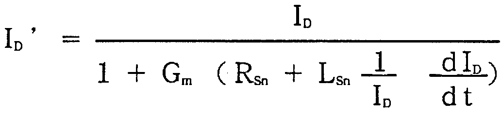
- FIG. 17 shows an equivalent circuit diagram of the transistor. If the wiring length for connecting the source and ground send level is increased, the parasitic resistance R e and parasitic Indakutansu L e is ignore
- the voltage drop in the source wiring is determined by the sum of the product of the parasitic resistance and the current and the product of the parasitic inductance and the time derivative of the current.
- the term of the time derivative of the current becomes large, and the parasitic inductance greatly contributes to the voltage drop.
- the problem of the parasitic resistance and the parasitic inductance also appears.
- FIG. 18 is a graph showing the relationship between the signal amplitude and the position when a high-frequency signal is applied from one end of the gate of the transistor in FIG. It shows how the voltage amplitude attenuates as the signal propagates through the gate electrode.
- the resistance of the gate electrode increases, high-frequency components are attenuated, and even if the gate width W is increased, it cannot be used effectively as a whole.
- Figure 19 shows the signal attenuation when the signal propagates 1 mm, 2 mm, 3 mm, and 4 mm on the wiring.
- electric field components directed in the signal propagation direction cause power consumption in the silicon substrate, causing significant waveform attenuation.
- the waveform of the high-speed signal propagating through the wiring is distorted, which has been a great barrier to high-speed operation.
- Fig. 20 shows an example of a commonly used method of forming an LDD structure as a countermeasure against a high electric field near the drain, which is one of the causes of degradation of device characteristics due to miniaturization.
- a polysilicon gate as a mask, after ion implantation of ⁇ relatively low concentrations (e.g. 1 X 1 0 13 cm one 2), depositing a CVDS I_ ⁇ 2 film. Then, a side wall is formed by isotropic mode reactive ion etching, and source Z drain ion implantation is performed.
- ⁇ relatively low concentrations e.g. 1 X 1 0 13 cm one 2
- the conventional transistor For example a gate insulating film (S io 2 ) Cannot be used due to the direct tunnel current of the insulating film.
- a transistor with a large gate width W for driving a large current is used, There is a problem that it takes a finite time to turn on the transistor from one end to the other, and the waveform of the high-speed signal transmitted through the wiring is broken.
- an object of the present invention is to provide a semiconductor device which has a large power driving capability and enables high-speed operation. Disclosure of the invention
- a first semiconductor region of a first conductivity type is provided on a metal substrate via a first insulating film, and a first semiconductor region of a second conductivity type is provided in the first semiconductor region.
- Source and drain regions are formed, and a first metal gate electrode is formed on a region separating the first source and drain regions via a second insulating film.
- a preferred embodiment of the present invention is a semiconductor device in which the second insulating film has a relative dielectric constant of 8 or more and a film thickness tj of the second insulating film satisfies the following expression (2).
- the second insulating film is formed by oxidizing the semiconductor region and an insulating film having a relative dielectric constant of 8 or more, and has a relative dielectric constant of 8 or more.
- This is a semiconductor device having a stacked structure with an oxide film having a thickness smaller than the thickness of an insulating film.
- the second insulating film is thickened at an end of the metal gate electrode, and oxidizes the first metal gate electrode to form the metal gate electrode.
- a semiconductor device in which an oxide of a metal constituting the metal gate is formed between an end of the metal gate and the second insulating film.
- the first semiconductor region has a thickness of 0.01 to 0.1 ⁇ m, and a distance between the source and drain regions is 0.25 ⁇ m or less. It is a semiconductor device.
- the first insulating film has a periodic step.
- at least one of the first insulating film, the first semiconductor region, and the second insulating film is a semiconductor formed by a dual frequency excitation sputtering method. It is a body device.
- a second semiconductor region of a second conductivity type is formed on the metal substrate via the first insulating film, and a first conductive region is formed in the second semiconductor region.
- a second source / drain region of a mold type, and the second metal gate electrode is formed on a region separating the second source / drain region via the second insulating film; This is a semiconductor device which is in contact with one of the metal gate electrodes.
- the impurity concentration in a portion of the first drain region adjacent to the first semiconductor region of the first conductivity type is lower than the impurity concentration in the first source region.
- the first source region is connected to the metal substrate by a metal wiring.
- the second source region is connected to a metal plate having a width larger than the metal wiring width above the second source region by a metal wiring. It is preferable that at least one of the substrate and the metal plate is provided with a mechanism through which a fluid flows. Action
- the present invention by forming a thin semiconductor layer on the metal substrate via the first insulating film, it is possible to suppress the attenuation of the signal waveform generated when the silicon substrate is used.
- the metal wiring on the metal substrate via the insulating film by providing the metal wiring on the metal substrate via the insulating film, the electric field component directed in the signal propagation direction is eliminated, and only the component perpendicular to the signal propagation direction is eliminated, thereby avoiding waveform attenuation.
- the thickness and the channel length of the semiconductor region of the present invention are preferably 0.11 to 0.1 ⁇ m and 0.25 ⁇ m, respectively. Within this range, signal waveform attenuation can be further suppressed, Further, the gate delay time can be reduced, and for example, an ultra-high-speed operation of 20 ps or less can be realized.
- the metal substrate may be a conductive material having high conductivity, and another substance may be present under the substrate.
- the first insulating film may be a material having a high thermal conductivity.
- Wide-gap semiconductors such as diamonds and SiC can also be used.
- the second insulating film having a relative dielectric constant of 8 or more is used.
- a dielectric constant of 25 Ta. 0 5 film is preferably used.
- a current approximately 7 times or more can flow in comparison with the conventional device using Sio 2 as the gate oxide film.
- miniaturization can be achieved in about 1/7.
- the present invention can realize a high current driving capability that cannot be realized in a conventional transistor using Sio 2 as a gate oxide film, and can achieve extremely miniaturization by the present invention.
- the current driving capability of the transistor can be increased.
- the large insulating film dielectric constant is equivalently possible to reduce the thickness of the S io 2. Therefore to define the equivalent oxide film thickness in the case of using a large insulating film dielectric constant (S io 2 terms) t '.
- the transistor using the SiO 2 gate oxide film has a high current driving capability that cannot be realized with a transistor using the SiO 2 gate oxide film. If the gate oxide film thickness satisfies Equation 2, it is possible to realize a high current driving capability that cannot be realized by a conventional semiconductor device.
- the dielectric constant of the gate insulating film 8 or higher to pass 3 nm thickness of S I_ ⁇ 2 conventional transistor and the current had use of the thickness of the gate oxide film, 6 nm or less Good on. Since the leakage current due to the direct tunneling phenomenon decreases exponentially with the film thickness, a gate insulating film of 6 nm or more has a sufficient margin for the leakage current due to the direct tunneling phenomenon. Therefore, the reliability of the transistor can be improved.
- These insulating films may be oxidized after forming the metal film, or may be formed directly as oxidized films.
- the second insulating film has an insulating film having a relative dielectric constant of 8 or more; It is preferable to have a laminated structure with the oxide film of the semiconductor.
- the interface state density of the semiconductor can be reduced, and a larger current can be driven.
- the thickness of the oxide film must be smaller than the thickness of the insulating film having a relative dielectric constant of 8 or more.
- the thickness of the insulating film below the end of the metal gate electrode is thicker than that of the central portion.
- the voltage concentration effect can be prevented, and the withstand voltage can be further increased.
- a metal having a small specific resistance is used as the gate electrode.
- signal amplitude attenuation can be greatly suppressed by using A1. Therefore, by using the A1 electrode, it is possible to drive over the entire gate width.
- a step of angstrom accuracy serving as a growth nucleus of silicon is provided on the surface of the first insulating film.
- the in-plane rotation direction of the silicon crystal grains can be made uniform, and a higher quality silicon single crystal can be obtained. That is, when a silicon film having a uniform rotation direction covers the surface of one layer on the first insulating film, the subsequent silicon atoms are deposited by obtaining information of the base, so that a single-crystal silicon layer is formed. At this time, the silicon atoms are given the optimum migration energy by the effect of the low-energy ion irradiation, and a single crystal film with no dense crystal defects can be obtained.
- 0.5 to 5.0 Onm are provided at a period of 0.2 to 5.0 // m, so that a higher quality silicon crystal can be formed.
- a material of the first insulating film As a material of the first insulating film, a material having high thermal conductivity is preferable, and A 1 N is particularly preferable. By using A 1 N with high thermal conductivity on a metal substrate, the heat generated by the transistor can be immediately released to the outside, resulting in lower thermal noise levels and improved circuit operation reliability .
- first and second insulating films and the semiconductor film of the present invention various vacuum film forming methods can be used.
- the device is preferably used.
- CMOS structure as a circuit type, so that a noise margin is increased even with a decrease in power supply voltage.
- heat generated by ultra-high-speed operation in CMOS is immediately released to the outside through the A1N insulating film with high thermal conductivity provided on the metal substrate and the metal substrate as described above.
- the thermal noise level which is the critical noise, has been reduced, and the reliability of circuit operation has been improved.
- FIG. 1 is a schematic sectional view of a semiconductor device according to a first embodiment.
- Figure 2 is a schematic diagram of a dual-frequency excitation plasma processing system.
- FIGS. 3 (a) and 3 (b) show various insulating films on which a single-crystal silicon layer is grown.
- FIG. 4 shows the drain current of the transistor according to Example 1 normalized by the gate length L and the gate width W. 4 is a graph showing the relationship between the voltage and the drain voltage.
- Fig. 5 is a graph showing the signal amplitude attenuation when a high-frequency signal is input from one end of the gate.
- FIG. 6 is a graph showing deterioration of a pulse waveform propagating at a normal temperature on a wiring provided on a metal substrate of the present invention via an insulating film on a metal substrate.
- Figure 7 relates to Example 2, a) is a schematic sectional view of a semiconductor device, (b) is a graph showing the difference in interface state with and without S io 2.
- FIGS. 8A and 8B relate to the third embodiment.
- FIG. 8A is a schematic cross-sectional view of a gate electrode end of a semiconductor device, and FIG. Graph shown.
- FIG. 9 is a schematic sectional view of a semiconductor device according to a fourth embodiment of the present invention.
- FIG. 10 is a schematic cross-sectional view showing a procedure for manufacturing the semiconductor device of FIG.
- FIG. 11 is a diagram showing drain current-voltage characteristics normalized by the gate length L and the gate width W.
- FIG. 12 is a schematic sectional view of a semiconductor device according to a fifth embodiment of the present invention.
- FIG. 13 is a diagram showing an output voltage waveform of the switching operation of the CMOS inverter of the present embodiment.
- FIG. 14 is a schematic sectional view of a semiconductor device showing a sixth embodiment of the present invention.
- FIG. 15 is a graph showing a relationship between power consumption and temperature rise measured by an IC chip having an area of 2 ⁇ 2 cm manufactured using the semiconductor device of this example.
- FIGS. 16A and 16B are schematic diagrams of a conventional semiconductor device.
- FIG. 16A is a plan view
- FIG. 16B is a cross-sectional view
- FIG. 16C is an equivalent circuit diagram.
- FIG. 17 is an equivalent circuit diagram of a conventional transistor.
- FIG. 18 is a graph showing how the signal amplitude attenuates when a high-frequency signal is input from the gate end in the apparatus of FIG.
- FIG. 19 is a graph showing the deterioration of a pulse waveform propagating on a wiring provided on a conventional silicon substrate via an insulating film at normal temperature.
- FIG. 20 is a diagram illustrating an example of a conventional method of forming an LDD structure.
- FIG. 1 is a sectional view of a semiconductor device according to a first embodiment of the present invention.
- an A 1 N (thermal conductivity: 18 OW / mK) insulating film (first insulating film) 102 is formed on a Cu substrate 101, and a single crystal is formed thereon.
- a silicon layer 103 was deposited to produce a CMOS inverter circuit.
- the gate oxide film (second insulating film) 104 is Ta 2 O 5 (relative permittivity: 25) with a thickness of 5 nm, and the gate electrode 105 is composed of A 1
- the A1 wiring 106 in contact with the source and drain regions and the gate electrode is insulated from other semiconductor regions via an insulating film.
- FIG. 2 shows a schematic diagram of a dual-frequency excitation plasma processing apparatus.
- the apparatus has a sample 108 inside the chamber 107 and a sample mounting portion placed in parallel with the sample 108, and is provided with a gas inlet 11 ° and a vacuum exhaust system 111.
- the RF power supply 112 used for plasma discharge is independently coupled to the target 108 and the sample 109 via a matching circuit 113 to control the self-bias of the sample 109. it can.
- shields 114 are provided so as to surround the electrodes, and the potential of the shields can be controlled by applying an external bias.
- the evacuation system 111 is composed of an oil-free magnetically levitated turbo-molecular pump and a dry pump, and the ultimate degree of vacuum in the chamber 107 achieves an ultra-high vacuum of the order of 10_1G .
- Ultra-high purity argon gas is supplied from the gas inlet 110.
- an A1N film is formed as a first insulating film on a Cu substrate to a thickness of 200 nm, and 2 ⁇ 2 m of various heights (0.5 to 11.4 nm) is formed by jet etching.
- a step was formed in which the convex portions of were periodically arranged at a gap of 1 m.
- Figure 3 shows the surface image of the A 1 N film.
- a high-resolution atomic force microscope which can be observed in ultra-high purity gas and ultra-high vacuum, was used to observe the shape of the steps on the atomic order.
- crystalline silicon was formed in the form of 0 ⁇ 01 to 0 ⁇ 1.
- the obtained crystalline silicon film was a single crystal film that was dense and had no crystal defects.
- a silicon film aligned in the rotating direction covers the surface of one layer on the insulating film, and the subsequent silicon atoms are deposited by obtaining the information of the base. It is believed that a con layer is formed. It is thought that the silicon atoms at this time are given the optimal migration energy by the effect of low energy ion irradiation, and a single crystal film without dense crystal defects can be obtained. In this example, a single crystal having fewer defects was obtained when the step was in the range of 0.5 to 5.0 nm.
- An insulating film T a 2 0 5 is formed over the single crystal silicon film 1 0 3, followed by A 1 0. 5 // After m formed, performs patterning of the gate electrode, the putter training source 'drain
- the source and drain were formed by ion implantation, and a MOS transistor was prototyped.
- the source / drain regions were formed by ion implantation in a self-aligned manner using the A1 gate electrode as a mask.
- the annealing of the ion-implanted layer was performed at a low temperature of 450 ° C.
- the ion implantation apparatus, 1 0 has a higher degree of vacuum than one 9 T orr, using ultra clean ion implantation apparatus which is designed to contamination with spa Ttaringu chamber metal material by the ion beam is sufficiently low.
- Figure 4 shows the relationship between drain current and drain voltage normalized by the gate length L and gate width W.
- the transistor of the present invention S i 0 2 to show that can flow is indeed about seven times the current than the conventional one used in a gate oxide film.
- This has a dielectric constant of gate one Bok voltage corresponds with what is T a 2 0 5 of the present invention is about 7 times the 3.9 of S i 0 2.
- the dielectric constant is increased about 7 times, and the gate capacitance per unit area is increased about 7 times, so that the channel carrier concentration that can be induced with the same voltage is also increased about 7 times, and the current that can flow is also increased. That was about a seven-fold increase.
- Figure 5 shows the results of comparison of the signal amplitude attenuation when a high-frequency signal is input from one end of the gate electrode between the conventional polycrystalline silicon electrode and the A1 electrode.
- the signal amplitude is significantly attenuated, whereas in the case of the A1 electrode, it is not so much attenuated. Therefore, by using the A1 electrode, it was possible to drive the entire gate width.
- Figure 6 shows the degradation of the pulse waveform propagating over the wiring provided on the metal substrate via the insulating film at room temperature. Attenuation of the signal waveform generated on a silicon substrate hardly occurs when a metal substrate is used. That is, by providing the metal wiring on the metal substrate with the insulating film interposed therebetween, the electric field component directed in the signal propagation direction is eliminated, and only the component perpendicular to the signal propagation direction is provided, thereby avoiding waveform attenuation.
- the MOSFET having a channel length of 0.25 m or less, and the thickness of Si is set to 0.06 / m, thereby achieving an ultra-high speed with a gate delay time of 20 ps or less. Operation has been confirmed.
- FIG. 7 shows a second embodiment of the present invention.
- FIG. 7A is a sectional view of a semiconductor device according to the present invention. Between the silicon thin film 2 0 1 and T a 2 0 5 film 2 0 2 Ru first gate one gate insulating film der, S I_ ⁇ 2 film 2 0 3 which is formed by oxidizing the substrate S i is ⁇ Has been entered.
- the SiO 2 film 203 was formed in an oxygen atmosphere at 300 ° C. Then a metal T a using two-frequency excitation plasma processing apparatus of FIG. 2, deposited by bias sputtering evening method, a T a 2 0 5 film 2 0 2 performs continuous direct oxidation without breaking vacuum Formed. Otherwise, the procedure of Example 1 was repeated to fabricate a CMOS Impa overnight.
- the interface between the silicon thin film and the gate insulator corresponds to a channel portion through which current flows
- the interface characteristics affect the device characteristics of the semiconductor device. For example, interface If the level density is large, the carriers in the channel will be scattered and the mobility will decrease. A decrease in mobility leads to a decrease in current drive capability. Therefore, the interface state density must be kept as low as possible.
- the thickness of the S i 0 2 film 2 0 3 is increased, T a 2 0 5 film 2 0 determined by the series combined capacitance of a 2 gate one preparative capacity is reduced, the high dielectric gate Ichito insulating film since the effect resulting in one such small, the thickness of the S i 0 9 film 2 0 3 has to be thinner than T a 2 0 5 film 2 0 2 as a first gate insulating film.
- FIG. 8 shows a third embodiment of the present invention.
- Figure 8 (a) shows a cross-sectional view of the gate electrode.
- 3 0 1 drain, 3 0 2 A 1 gate electrode, 3 0 3 shows a T a n O c.
- the surface of the A1 gate electrode was post-oxidized by anodization.
- the gate electrode end portion 3 0 4 bites oxide A 1 2 0 3 of A 1 occurs, the gate insulating film thickness of this portion was found to be thicker than the flat portion 3 0 5 .
- FIG. 8 (b) shows the relationship between the thickness of the oxide film formed by the anodic oxidation method and the breakdown voltage of the gate insulating film.
- the withstand voltage of the gate insulating film is about 4 ⁇ cm. ing.
- Post-oxidation film 5 nm, and the improvement of the withstand voltage was almost the same thickness as gate insulating film T a 2 0 5 is saturated. Breakdown voltage at this time, about 5. 5 MV / cm can be said to be T a 2 0 5 of the intrinsic breakdown voltage used here. In other words, it indicates that the electric field concentration effect (edge effect) at the gate electrode edge can be completely prevented.
- the first gate insulating film (second insulating film) was used T a Ri O c as 3 0 3, A 1 2 0 . Needless to say, this may be the case. Further, the post-oxidation film, the A 1 gate one Bok electrode was used A 1 2 0 3 anodized, the gate electrode end portion Any other insulating film can be used as long as it can increase the thickness of the insulating film.
- FIG. 9 shows a fourth embodiment of the present invention.
- the LDD structure is formed only in the drain portion.
- FIG. 1 One example of realizing this structure is shown in FIG. First, a resist layer having an opening only in the drain region is formed by lithography. Next, an oxide film is formed only in the opened drain region, and a side wall is formed only in the drain region by isotropic mode reactive ion etching. The resist is stripped and source Z drain ion implantation is performed.
- Figure 11 shows the drain current-voltage characteristics normalized by the gate length L and the gate width W. It can be seen that at the same drain voltage, the transistor having the LDD structure only in the drain region according to the present invention can flow almost twice as much current as the transistor having the conventional LDD structure. This is because the transistor of the present invention does not have the parasitic resistance in the low-concentration layer in the source region, which was present in the conventional LDD structure, so that there is no voltage drop in the source region and high current driving capability can be obtained. It shows that. As for the withstand voltage, almost the same result as the conventional LDD structure was obtained.
- the parasitic resistance in the source region is reduced, and the electric field relaxation effect near the drain is sufficiently provided to achieve high reliability and high current driving capability. Can be realized.
- FIG. 12 shows a fifth embodiment of the present invention.
- a CMOS configuration in which the source 1203 of the n-type MOS transistor is connected to the Cu substrate 1201 directly below, and the source 1202 of the p-type MOS transistor is connected to the Cu wiring 1204 directly above
- An inverter circuit was prototyped. The other detailed description is the same as in the first embodiment, and will not be repeated.
- the Cu substrate 1 201 is grounded, and the Cu wiring 1204 is connected to the power supply voltage. In this case, the area of the Cu wiring 1204 was set to 2/3 of the chip area.
- FIG. 13 shows the output voltage of the switching operation of the CMOS inverter in this embodiment. 3 shows a pressure waveform.
- the transistor of the present invention obtains an almost ideal output waveform as compared with the conventional one shown by the dotted line in the source wiring diagram 9. This is because, in the conventional transistor, the parasitic resistance of the source wiring cannot be ignored, and the effective current driving capability is reduced.
- the parasitic resistance of the source wiring This corresponds to the fact that the parasitic inductance is negligible and high current drive capability is realized. That is, with the transistor of the present invention, high current driving capability was achieved, and the delay time of the switching operation was successfully reduced as much as possible.
- FIG. 14 is a sectional view of a semiconductor device according to a sixth embodiment of the present invention. Grooves through which water flows are made in the metal substrate. At this time, the flow rate of water is 6 mZ sec, the number of grooves is 200 in a 2 x 2 cm chip, and the size of the grooves is 5 // m square.
- FIG. 15 shows the relationship between power consumption and temperature rise measured by an IC chip having an area of 2>: 2 cm manufactured using the semiconductor device of this example.
- the power consumption is 1-0 W
- the temperature rise of the conventional IC chip is 200 ° C
- the temperature rise of the IC chip incorporating the semiconductor device of the present invention is 25 ° C. ing.
- the thermal noise level that increases in proportion to the temperature rise can be kept low, and an ultra-high-speed operation and a highly accurate switching operation can be realized.
- performance degradation such as a change in transistor threshold and a decrease in mobility due to a rise in temperature was also minimized.
- a semiconductor device is provided with a first conductive type first semiconductor region on a metal substrate via a first insulating film, and a second conductive type second semiconductor region is provided in the first semiconductor region.
- One source and drain region is formed, and the first source and drain region is further formed.
- a structure in which the first metal gate electrode is formed on the region separating the first and second insulating films via the second insulating film makes it possible to provide a semiconductor device having a large current driving capability and capable of high-speed operation .
- the interface state density of the semiconductor layer can be reduced, and the current driving capability can be further enhanced.
- the withstand voltage of the gate insulating film can be further improved, and a larger current drive can be performed.
- high reliability and high current driving capability can be realized by reducing the parasitic resistance in the source region and sufficiently reducing the electric field in the vicinity of the drain.
- the thermal noise level which increases in proportion to the temperature rise can be kept low, and the switching operation can be realized with ultra-high speed operation and high accuracy.
- performance degradation such as a change in transistor threshold value and a decrease in mobility due to a rise in temperature can be minimized.
Landscapes
- Thin Film Transistor (AREA)
- Insulated Gate Type Field-Effect Transistor (AREA)
- Metal-Oxide And Bipolar Metal-Oxide Semiconductor Integrated Circuits (AREA)
- Bipolar Transistors (AREA)
Description
Claims
Priority Applications (2)
| Application Number | Priority Date | Filing Date | Title |
|---|---|---|---|
| US08/454,324 US5650650A (en) | 1992-12-24 | 1993-12-21 | High speed semiconductor device with a metallic substrate |
| EP94903034A EP0709897A4 (en) | 1992-12-24 | 1993-12-21 | SEMICONDUCTOR ARRANGEMENT |
Applications Claiming Priority (4)
| Application Number | Priority Date | Filing Date | Title |
|---|---|---|---|
| JP4/343030 | 1992-12-24 | ||
| JP34303092 | 1992-12-24 | ||
| JP4/181998 | 1993-06-28 | ||
| JP18199893A JP3339730B2 (ja) | 1992-12-24 | 1993-06-28 | 半導体装置 |
Publications (1)
| Publication Number | Publication Date |
|---|---|
| WO1994015366A1 true WO1994015366A1 (fr) | 1994-07-07 |
Family
ID=26500965
Family Applications (1)
| Application Number | Title | Priority Date | Filing Date |
|---|---|---|---|
| PCT/JP1993/001850 Ceased WO1994015366A1 (fr) | 1992-12-24 | 1993-12-21 | Dispositif a semiconducteurs |
Country Status (4)
| Country | Link |
|---|---|
| US (1) | US5650650A (ja) |
| EP (1) | EP0709897A4 (ja) |
| JP (1) | JP3339730B2 (ja) |
| WO (1) | WO1994015366A1 (ja) |
Families Citing this family (14)
| Publication number | Priority date | Publication date | Assignee | Title |
|---|---|---|---|---|
| KR100253699B1 (ko) * | 1996-06-29 | 2000-05-01 | 김영환 | Soi소자 및 그 제조방법 |
| EP0895282A3 (en) | 1997-07-30 | 2000-01-26 | Canon Kabushiki Kaisha | Method of preparing a SOI substrate by using a bonding process, and SOI substrate produced by the same |
| DE19856084C2 (de) * | 1998-12-04 | 2002-07-11 | Infineon Technologies Ag | Verfahren zur Herstellung einer Metalloxidschicht bzw. einer strukturierten Metalloxidschicht |
| JP2003069013A (ja) * | 2001-08-29 | 2003-03-07 | Hitachi Ltd | 半導体装置及びその製造方法 |
| CN1328811C (zh) | 2002-01-29 | 2007-07-25 | 松下电器产业株式会社 | 具有燃料电池的半导体装置及其制造方法 |
| JP4904482B2 (ja) * | 2005-01-18 | 2012-03-28 | 国立大学法人東北大学 | 半導体装置 |
| MX354786B (es) | 2007-06-04 | 2018-03-21 | Synergy Pharmaceuticals Inc | Agonistas de guanilato ciclasa utiles para el tratamiento de trastornos gastrointestinales, inflamacion, cancer y otros trastornos. |
| US8969514B2 (en) | 2007-06-04 | 2015-03-03 | Synergy Pharmaceuticals, Inc. | Agonists of guanylate cyclase useful for the treatment of hypercholesterolemia, atherosclerosis, coronary heart disease, gallstone, obesity and other cardiovascular diseases |
| ES2522968T3 (es) | 2008-06-04 | 2014-11-19 | Synergy Pharmaceuticals Inc. | Agonistas de guanilato ciclasa útiles para el tratamiento de trastornos gastrointestinales, inflamación, cáncer y otros trastornos |
| AU2009270833B2 (en) | 2008-07-16 | 2015-02-19 | Bausch Health Ireland Limited | Agonists of guanylate cyclase useful for the treatment of gastrointestinal, inflammation, cancer and other disorders |
| US9616097B2 (en) | 2010-09-15 | 2017-04-11 | Synergy Pharmaceuticals, Inc. | Formulations of guanylate cyclase C agonists and methods of use |
| AU2014235215A1 (en) | 2013-03-15 | 2015-10-01 | Synergy Pharmaceuticals Inc. | Agonists of guanylate cyclase and their uses |
| AU2014235209B2 (en) | 2013-03-15 | 2018-06-14 | Bausch Health Ireland Limited | Guanylate cyclase receptor agonists combined with other drugs |
| BR112015030326A2 (pt) | 2013-06-05 | 2017-08-29 | Synergy Pharmaceuticals Inc | Agonistas ultrapuros de guanilato ciclase c, método de fabricar e usar os mesmos |
Citations (7)
| Publication number | Priority date | Publication date | Assignee | Title |
|---|---|---|---|---|
| JPS5856466A (ja) * | 1981-09-30 | 1983-04-04 | Toshiba Corp | 薄膜電界効果トランジスタ |
| JPS59210671A (ja) * | 1983-05-14 | 1984-11-29 | Nippon Telegr & Teleph Corp <Ntt> | シリコン薄膜電界効果トランジスタ |
| JPS60200564A (ja) * | 1984-03-24 | 1985-10-11 | Mitsubishi Electric Corp | 薄膜半導体素子集積回路装置 |
| JPS61276256A (ja) * | 1985-05-30 | 1986-12-06 | Fujitsu Ltd | 半導体装置 |
| JPS6486543A (en) * | 1987-09-29 | 1989-03-31 | Hitachi Ltd | Semiconductor mounting cooling structure |
| JPH0374880A (ja) * | 1989-08-16 | 1991-03-29 | Matsushita Electron Corp | 半導体装置 |
| JPH04360580A (ja) * | 1991-06-07 | 1992-12-14 | Casio Comput Co Ltd | 電界効果型トランジスタおよびその製造方法 |
Family Cites Families (6)
| Publication number | Priority date | Publication date | Assignee | Title |
|---|---|---|---|---|
| JPS57177559A (en) * | 1981-04-24 | 1982-11-01 | Fujitsu Ltd | Semiconductor device and manufacture thereof |
| EP0181091B1 (en) * | 1984-11-02 | 1990-06-13 | Kabushiki Kaisha Toshiba | Schottky gate field effect transistor and manufacturing method thereof |
| US5164805A (en) * | 1988-08-22 | 1992-11-17 | Massachusetts Institute Of Technology | Near-intrinsic thin-film SOI FETS |
| US5289027A (en) * | 1988-12-09 | 1994-02-22 | Hughes Aircraft Company | Ultrathin submicron MOSFET with intrinsic channel |
| JPH0395922A (ja) * | 1989-09-07 | 1991-04-22 | Canon Inc | 半導体薄膜の形成方法 |
| JP2744126B2 (ja) * | 1990-10-17 | 1998-04-28 | 株式会社東芝 | 半導体装置 |
-
1993
- 1993-06-28 JP JP18199893A patent/JP3339730B2/ja not_active Expired - Lifetime
- 1993-12-21 WO PCT/JP1993/001850 patent/WO1994015366A1/ja not_active Ceased
- 1993-12-21 US US08/454,324 patent/US5650650A/en not_active Expired - Lifetime
- 1993-12-21 EP EP94903034A patent/EP0709897A4/en not_active Withdrawn
Patent Citations (7)
| Publication number | Priority date | Publication date | Assignee | Title |
|---|---|---|---|---|
| JPS5856466A (ja) * | 1981-09-30 | 1983-04-04 | Toshiba Corp | 薄膜電界効果トランジスタ |
| JPS59210671A (ja) * | 1983-05-14 | 1984-11-29 | Nippon Telegr & Teleph Corp <Ntt> | シリコン薄膜電界効果トランジスタ |
| JPS60200564A (ja) * | 1984-03-24 | 1985-10-11 | Mitsubishi Electric Corp | 薄膜半導体素子集積回路装置 |
| JPS61276256A (ja) * | 1985-05-30 | 1986-12-06 | Fujitsu Ltd | 半導体装置 |
| JPS6486543A (en) * | 1987-09-29 | 1989-03-31 | Hitachi Ltd | Semiconductor mounting cooling structure |
| JPH0374880A (ja) * | 1989-08-16 | 1991-03-29 | Matsushita Electron Corp | 半導体装置 |
| JPH04360580A (ja) * | 1991-06-07 | 1992-12-14 | Casio Comput Co Ltd | 電界効果型トランジスタおよびその製造方法 |
Non-Patent Citations (2)
| Title |
|---|
| See also references of EP0709897A4 * |
| SEIJIRO FURUKAWA, "SOI structuring technology", 23 October 1987 (23.10.87), Sangyo Tosho K.K., p. 14-15. * |
Also Published As
| Publication number | Publication date |
|---|---|
| EP0709897A4 (en) | 1997-05-28 |
| JP3339730B2 (ja) | 2002-10-28 |
| JPH06244416A (ja) | 1994-09-02 |
| EP0709897A1 (en) | 1996-05-01 |
| US5650650A (en) | 1997-07-22 |
Similar Documents
| Publication | Publication Date | Title |
|---|---|---|
| US6255731B1 (en) | SOI bonding structure | |
| US8232597B2 (en) | Semiconductor-on-insulator with back side connection | |
| US7235822B2 (en) | Transistor with silicon and carbon layer in the channel region | |
| KR100614822B1 (ko) | 〈110〉 면방위의 실리콘 표면상에 형성된 반도체 장치 및그 제조 방법 | |
| US5420048A (en) | Manufacturing method for SOI-type thin film transistor | |
| WO1994015366A1 (fr) | Dispositif a semiconducteurs | |
| CN102576692A (zh) | 具有背侧体区连接的绝缘体上半导体 | |
| WO1993023878A1 (fr) | Dispositif semiconducteur | |
| CN1536679A (zh) | 半导体结构 | |
| JP4105353B2 (ja) | 半導体装置 | |
| JP4623451B2 (ja) | 半導体基板及びその作製方法 | |
| US6756637B2 (en) | Method of controlling floating body effects in an asymmetrical SOI device | |
| CN117976672A (zh) | 一种高电学性能三维互补场效应晶体管及其制备方法 | |
| CN111048523A (zh) | 阵列基板及其制备方法 | |
| WO2025252253A1 (zh) | 一种二维半导体器件及其制备方法 | |
| Sung et al. | Deep-submicron channel length oxide semiconductor thin-film transistors enabled by self-aligned nanogap lithography | |
| Teng et al. | Thin-film transistors on plastic and glass substrates using silicon deposited by microwave plasma ECR-CVD | |
| Xiong et al. | A novel self-aligned offset-gated polysilicon TFT using high-/spl kappa/dielectric spacers | |
| JP2007123702A (ja) | 薄膜トランジスタとその製造方法 | |
| TW202541641A (zh) | 與p通道耦接的n通道以及製造方法 | |
| Serikawa et al. | High-mobility poly-Si thin film transistors fabricated on stainless-steel foils by low-temperature processes using sputter-depositions | |
| CN115188820B (zh) | 基于InN/AlGaN/GaN异质结的p沟道金属氧化物半导体场效应管及制备方法 | |
| US20130270680A1 (en) | Method for forming semiconductor devices with active silicon height variation | |
| JPH0322064B2 (ja) | ||
| CN1450657A (zh) | 一种垂直型大功率场效应晶体管单元结构 |
Legal Events
| Date | Code | Title | Description |
|---|---|---|---|
| AK | Designated states |
Kind code of ref document: A1 Designated state(s): US |
|
| AL | Designated countries for regional patents |
Kind code of ref document: A1 Designated state(s): AT BE CH DE DK ES FR GB GR IE IT LU MC NL PT SE |
|
| DFPE | Request for preliminary examination filed prior to expiration of 19th month from priority date (pct application filed before 20040101) | ||
| 121 | Ep: the epo has been informed by wipo that ep was designated in this application | ||
| WWE | Wipo information: entry into national phase |
Ref document number: 1994903034 Country of ref document: EP |
|
| WWE | Wipo information: entry into national phase |
Ref document number: 08454324 Country of ref document: US |
|
| WWP | Wipo information: published in national office |
Ref document number: 1994903034 Country of ref document: EP |
|
| WWW | Wipo information: withdrawn in national office |
Ref document number: 1994903034 Country of ref document: EP |