WO2009081663A1 - Filtre d'élimination de bande et connecteur doté de ce filtre - Google Patents
Filtre d'élimination de bande et connecteur doté de ce filtre Download PDFInfo
- Publication number
- WO2009081663A1 WO2009081663A1 PCT/JP2008/070409 JP2008070409W WO2009081663A1 WO 2009081663 A1 WO2009081663 A1 WO 2009081663A1 JP 2008070409 W JP2008070409 W JP 2008070409W WO 2009081663 A1 WO2009081663 A1 WO 2009081663A1
- Authority
- WO
- WIPO (PCT)
- Prior art keywords
- electrodes
- electrode
- band elimination
- elimination filter
- signal line
- Prior art date
- Legal status (The legal status is an assumption and is not a legal conclusion. Google has not performed a legal analysis and makes no representation as to the accuracy of the status listed.)
- Ceased
Links
Images


Classifications
-
- H—ELECTRICITY
- H01—ELECTRIC ELEMENTS
- H01P—WAVEGUIDES; RESONATORS, LINES, OR OTHER DEVICES OF THE WAVEGUIDE TYPE
- H01P1/00—Auxiliary devices
- H01P1/20—Frequency-selective devices, e.g. filters
-
- H—ELECTRICITY
- H01—ELECTRIC ELEMENTS
- H01G—CAPACITORS; CAPACITORS, RECTIFIERS, DETECTORS, SWITCHING DEVICES, LIGHT-SENSITIVE OR TEMPERATURE-SENSITIVE DEVICES OF THE ELECTROLYTIC TYPE
- H01G4/00—Fixed capacitors; Processes of their manufacture
- H01G4/35—Feed-through capacitors or anti-noise capacitors
-
- H—ELECTRICITY
- H01—ELECTRIC ELEMENTS
- H01G—CAPACITORS; CAPACITORS, RECTIFIERS, DETECTORS, SWITCHING DEVICES, LIGHT-SENSITIVE OR TEMPERATURE-SENSITIVE DEVICES OF THE ELECTROLYTIC TYPE
- H01G4/00—Fixed capacitors; Processes of their manufacture
- H01G4/38—Multiple capacitors, i.e. structural combinations of fixed capacitors
-
- H—ELECTRICITY
- H01—ELECTRIC ELEMENTS
- H01R—ELECTRICALLY-CONDUCTIVE CONNECTIONS; STRUCTURAL ASSOCIATIONS OF A PLURALITY OF MUTUALLY-INSULATED ELECTRICAL CONNECTING ELEMENTS; COUPLING DEVICES; CURRENT COLLECTORS
- H01R13/00—Details of coupling devices of the kinds covered by groups H01R12/70 or H01R24/00 - H01R33/00
- H01R13/66—Structural association with built-in electrical component
- H01R13/719—Structural association with built-in electrical component specially adapted for high frequency, e.g. with filters
- H01R13/7197—Structural association with built-in electrical component specially adapted for high frequency, e.g. with filters with filters integral with or fitted onto contacts, e.g. tubular filters
Definitions
- the present invention relates to a band elimination filter technique for removing electromagnetic waves of a specific frequency, and more particularly to a band elimination filter technique using a metamaterial.
- Patent Document 1 discloses a collector-mounted noise filter including a substrate made of a radio wave absorbing material and having front and back surfaces parallel to each other. The substrate is formed with a plurality of through holes penetrating the substrate. JP 2000-223881 A
- the frequency band that can be removed by these filters is limited. For example, since ferrite cannot remove electromagnetic waves in the GHz band or higher, it cannot be used for applications such as passing 2.4 GHz electromagnetic waves and removing 5 GHz electromagnetic waves.
- the present invention has been made to solve the above problems, and an object of the present invention is to provide a band elimination filter and a connector with a band elimination filter that can sharply remove electromagnetic waves of a target frequency.
- the present invention is a band elimination filter that removes a specific frequency component of a current flowing through a signal line, and includes a metamaterial arranged radially with the signal line as an axis. It arrange
- the metamaterial includes a plurality of electrode pairs each including a first electrode and a second electrode facing each other via an insulator, and a connection body that electrically connects the first electrode and the second electrode,
- the electrode surfaces of the first and second electrodes are arranged so as to be substantially parallel to the magnetic field lines formed by the current.
- connection body is disposed so as not to prevent a magnetic field line formed by an electric current from passing through a space sandwiched between the first and second electrodes.
- connection body includes two external electrodes formed to face each other in parallel, and the electrode surfaces of the two external electrodes are arranged so as to be substantially parallel to the magnetic force lines formed by the current. Has been.
- the metamaterial includes a plurality of plate electrodes arranged in parallel to each other via an insulator, a first connection electrode electrically connected to an even-numbered plate electrode of the plurality of plate electrodes, and a plurality of plates.
- a second connection electrode electrically connected to the odd-numbered plate electrode of the electrode, each electrode surface of the first and second connection electrode is formed perpendicular to the electrode surface of the plurality of plate electrodes,
- the electrode surfaces of the plurality of plate electrodes are arranged so as to be substantially parallel to the magnetic field lines formed by the current.
- the metamaterial includes first and second comb electrodes each having a plurality of electrode surfaces parallel to each other, the uppermost electrode surface of the first comb electrode and the uppermost layer of the second comb electrode.
- the electrode surface is formed in parallel with a predetermined interval, and the lowermost electrode surface of the first comb electrode and the lowermost electrode surface of the second comb electrode are parallel with a predetermined interval.
- the electrode surfaces of the first and second comb electrodes are formed so as to face each other, and are arranged so as to be substantially parallel to the magnetic field lines formed by the current.
- a donut plate standing upright with respect to the signal line is further provided, and the metamaterial is fixed on the donut plate.
- the metamaterial has a plurality of cylindrical electrodes having cylindrical surfaces with different diameters around the signal line, and a first connection electrically connected to the even-numbered cylindrical electrodes of the plurality of cylindrical electrodes. And an electrode and a second connection electrode electrically connected to an odd-numbered cylindrical electrode of the plurality of cylindrical electrodes.
- the metamaterial includes a plurality of base materials, and the base material is electrically connected to the first and second electrodes, and the first and second electrodes each facing each other with an insulator interposed therebetween.
- the body is formed.
- the present invention is a band elimination filter that removes a specific frequency component of a current flowing through a signal line, and includes a metamaterial arranged radially with the signal line as an axis.
- the electrode surface of each said 2nd electrode is arrange
- the present invention according to yet another aspect is a band elimination filter that removes a specific frequency component of a current flowing through a signal line, and includes a metamaterial arranged radially with the signal line as an axis.
- a plurality of second electrodes facing each of the first internal electrodes, and a connection body for electrically connecting the plurality of first electrodes and the plurality of second internal electrodes, each of the first electrodes and The electrode surface of the second electrode is disposed so as to be orthogonal to the signal line.
- the length along the signal line of the metamaterial is formed to be shorter than 1 ⁇ 4 of one wavelength corresponding to a predetermined frequency component.
- the present invention according to still another aspect is a connector with a band elimination filter that incorporates the band elimination filter described above.
- a specific frequency component of an electromagnetic wave can be abruptly attenuated by the metamaterial arranged around the electric wire.
- FIG. 2 is a diagram illustrating a configuration of a filter 100.
- FIG. 2 is a diagram illustrating a configuration of a multilayer capacitor 110.
- FIG. 2 is a diagram illustrating a configuration of a multilayer capacitor 110.
- FIG. It is sectional drawing of the filter 100 which makes the surface containing the signal line 120 a cut surface.
- 6 is a diagram for explaining another arrangement example of the multilayer capacitor 110.
- FIG. It is the figure which showed the relationship between arrangement
- 2 is a diagram illustrating a configuration of a filter 200.
- FIG. 3 is a perspective view of a filter 300.
- FIG. 4 is a cross-sectional view of the filter 300.
- FIG. 4 is a perspective view of a filter 400.
- FIG. It is sectional drawing of the filter 400 which makes a plane containing an axis
- FIG. 4 is a cross-sectional view of the filter 400 in the radial direction.
- FIG. 6 shows how the filter 100 is inserted into the connector 1300.
- FIG. 4 is a four-quadrant diagram showing characteristics appearing with respect to an incident wave to a medium according to signs of magnetic permeability ⁇ and dielectric constant ⁇ . It is a figure for demonstrating the resonant circuit formed with a resonator in a resonant frequency.
- the present invention provides a band elimination filter that performs band elimination of current using a metamaterial or a connector with a band elimination filter.
- a metamaterial is an artificial material having electromagnetic or optical characteristics that a substance existing in nature does not have.
- Typical properties of such metamaterials include negative permeability ( ⁇ ⁇ 0), negative dielectric constant ( ⁇ ⁇ 0), or negative refractive index (when both permeability and dielectric constant are negative) Is mentioned.
- the region of ⁇ ⁇ 0 and ⁇ > 0, or the region of ⁇ > 0 and ⁇ ⁇ 0 is also referred to as “evanescent solution region”, and the region of ⁇ ⁇ 0 and ⁇ ⁇ 0 is also referred to as “left-handed region”.
- FIG. 14 is a four-quadrant diagram showing characteristics appearing with respect to an incident wave to the medium for each sign of magnetic permeability ⁇ and dielectric constant ⁇ .
- Most of the substances existing in the natural world correspond to the right-handed medium located in the first quadrant shown in FIG. 14, and the wave incident on the medium is refracted by the refractive index determined by the magnetic permeability and the dielectric constant, Propagate in the incident direction.
- the incident wave cannot propagate in the second quadrant and the fourth quadrant (evanescent solution region) shown in FIG.
- the third region left-handed region shown in FIG. 14 since the refractive index is negative, the wave incident on the medium propagates in the direction opposite to the incident direction.
- unnecessary electromagnetic waves radiated from electronic devices can be suppressed. That is, when a magnetic flux is incident on a medium that exhibits negative permeability, unnecessary electromagnetic waves radiated from an electronic device or the like can be reflected or suppressed.
- a device (typically a multilayer capacitor) including a plurality of electrodes arranged at a predetermined distance from each other is used as a metamaterial.
- a resonance circuit mainly composed of a capacitance generated between the electrodes is formed.
- This resonance circuit is sensitive to a specific frequency component of an electromagnetic wave generated by an alternating current flowing through the conductor, and can generate an electrical resonance phenomenon by receiving the electromagnetic wave of this frequency component. Due to this resonance phenomenon, a magnetic flux in the direction opposite to the magnetic flux applied to the resonant circuit is generated, and this generated magnetic flux induces an electric field in a direction that cancels the electric field generated by the current flowing through the conductor. As a result, as a whole, electromagnetic waves radiated from the conductor are reflected or suppressed.
- the device as described above is referred to as a resonator.
- FIG. 15 is a diagram for explaining a resonance circuit formed by the resonator 10 at the resonance frequency.
- the resonator 10 is described as a multilayer capacitor, but the mechanism for forming a resonance circuit is the same for other devices.
- first internal electrodes 12a and 13a, second internal electrodes 12b and 13b, and first external electrode 11a arranged such that their electrode surfaces are substantially parallel to the magnetic field lines of the magnetic field.
- the 2nd external electrode 11b acts as a coil (inductor) according to the path
- the uppermost layer electrode 12a, the first outer electrode 11a, and the lowermost layer electrode 13a of the first inner electrodes are electrically connected to each other and include these.
- a current path is formed.
- the uppermost layer electrode 12b, the second outer electrode 11b, and the lowermost layer electrode 13b of the second internal electrodes are also electrically connected to each other, and a current path including these is connected. It is formed.
- both current paths are electrically connected to each other via the electrostatic capacitance (capacitance C1) between the electrodes 12a and 12b and the electrostatic capacitance (capacitance C2) between the electrodes 13a and 13b.
- a resonant circuit is formed which is connected and includes capacitances C1 and C2 and inductances L1 to L6 generated by the respective electrodes. Therefore, the resonator 10 according to the present embodiment has a resonance frequency determined by the capacitance (C1 + C2) and the inductance (L1 + L2 + L3 + L4 + L5 + L6), and the magnetic resonance at the resonance frequency is generated when an electromagnetic wave having this resonance frequency is incident.
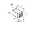
- FIG. 1A is a diagram illustrating a configuration of the filter 100.
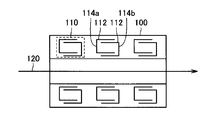
- the filter 100 includes a plurality of multilayer capacitors 110.
- the multilayer capacitors 110 are arranged radially on the cylindrical side surface with the signal line 120 as an axis.
- the multilayer capacitor 110 is fixed by an exterior part 130 that is a non-magnetic material.
- a resin material such as Teflon (registered trademark) is suitable.
- a ground (not shown) may be disposed on the outer side surface of the exterior part 130.
- FIG. 1B and FIG. 2 are diagrams each showing a configuration of the multilayer capacitor 110.
- the multilayer capacitor 110 includes a plurality of internal electrodes 112, a first external electrode 114a, and a second external electrode 114b.
- the internal electrodes 112 are alternately drawn from the first external electrode 114a and the second external electrode 114b.
- the internal electrode 112 connected to the first external electrode 114a and the internal electrode 112 connected to the second external electrode 114b form an electrode pair.
- the internal electrodes are drawn so as to be intentionally visible for easy understanding.
- the electrode surface of the internal electrode 112 is generated by a current 140 flowing through the signal line 120, as shown in FIG. 1 and FIG. 3, which is a cross-sectional view of the filter 100 viewed from the surface including the signal line 120.
- the magnetic field lines 150 are arranged so as to be substantially parallel to the magnetic field lines 150. That is, the electrode surface of the internal electrode 112 is disposed so as to surround the signal line 120 with the signal line 120 as an axis.
- the electrode surfaces of the first external electrode 114 a and the second external electrode 114 b are arranged so as to be substantially parallel to the magnetic force lines 150 generated by the current 140 flowing through the signal line 120. That is, the electrode surfaces of the first external electrode 114 a and the second external electrode 114 b are arranged so as to be orthogonal to the signal line 120.
- These external electrodes are not electrically connected to the signal line 120 or the ground.
- the multilayer capacitor 110 exhibits negative magnetic permeability. That is, the multilayer capacitor 110 exhibits negative magnetic permeability at a resonance frequency determined by the structure and arrangement of the multilayer capacitor 110. For this reason, propagation of the electromagnetic field of resonance frequency is inhibited.
- the multilayer capacitor 110 When the current 140 flows through the signal line 120, the multilayer capacitor 110 receives a specific frequency component (resonance frequency) of the electromagnetic wave generated by the current and resonates. Due to the resonance in the multilayer capacitor 110, a reverse magnetic flux is generated inside the multilayer capacitor 110, and an electric field induced by the generated magnetic flux prevents an electromagnetic wave generated by the current. As a result, in the signal line 120, the flow of the alternating current of the resonance frequency component in the multilayer capacitor 110 is hindered. That is, the filter 100 functions as a band cutoff filter that blocks the resonance frequency component of the multilayer capacitor 110.
- the length l ′ in the propagation direction of the current 140 in the signal line 120 of the multilayer capacitor 110 is at least with respect to the wavelength ⁇ of the electromagnetic wave at the resonance frequency. It must be shorter than ⁇ / 4. Furthermore, the length l ′ of the multilayer capacitor 110 is preferably ⁇ / 20 or less.
- ⁇ / 4 length l ′
- ⁇ 6.4 mm.
- fmax 46.875 GHz in the air. Therefore, it can be seen that when the multilayer capacitors 110 are arranged at a pitch of ⁇ / 4 or less, they function as gigahertz band metamaterials that cannot be realized with ferrite.
- the length l of the resonator can be appropriately designed according to the frequency region to be applied.
- the multilayer capacitor 110 has eight layers, but the number of layers is not limited to this. However, at least two electrode pairs are necessary to form a resonant circuit.
- the number of multilayer capacitors 110 is not limited to that shown in FIG.
- FIG. 1 shows an example in which the multilayer capacitor groups arranged radially around the signal line 120 are arranged over three stages, but the number of stages can be changed as appropriate. Attenuation can be increased by increasing the number of stages.
- FIG. 6 is a graph showing the relationship between the frequency and relative permeability with respect to the capacitance or the number of stages of several types of capacitors.
- the relative magnetic permeability represents a ratio of magnetic permeability to vacuum magnetic permeability. It can be seen that the change in relative permeability is greater when five stages of 47 pF multilayer capacitors are formed than when five stages are formed.
- each multilayer capacitor group is composed of eight multilayer capacitors 110, but the number can be changed.
- the resonance frequency can be changed by changing the capacitance of the multilayer capacitor.
- the resonant frequencies for the 47 pF, 68 pF, and 100 pF multilayer capacitors 110 are different.
- FIG. 4 is a diagram for explaining another arrangement example of the multilayer capacitor 110.
- 4 is a cross-sectional view of the filter 100 as seen in a plane including the signal line 120, as in FIG. That is, the electrode surface of the internal electrode 112 is arranged in a direction substantially orthogonal to the signal line 120, and the electrode surfaces of the first external electrode 114 a and the second external electrode 114 b are arranged in a direction parallel to the signal line 120. May be.
- the electrode surfaces of the internal electrode 112 and the first external electrode 114a and the second external electrode 114b are arranged so as to be parallel to the magnetic field lines of the magnetic field generated by the current flowing through the signal line 120.
- the negative magnetic permeability which is a function as a metamaterial, can be expressed.
- a negative magnetic permeability is also exhibited by being arranged so as to be substantially parallel to the magnetic field lines.
- substantially parallel means to exclude the state in which each electrode surface is orthogonal to the magnetic field lines of magnetic force, and in addition to the state in which each electrode surface is completely parallel to the magnetic field lines of magnetic field, Including a state having a predetermined angle. Practically, if the magnitude of the negative magnetic permeability expressed in the filter 100 is a value that can satisfy the requirements of the application, etc., it can be regarded as “substantially parallel”.
- FIG. 5 is a diagram showing a result of simulating frequency characteristics of relative permeability generated in multilayer capacitor 110 according to the first embodiment of the present invention for each orientation of multilayer capacitor 10.
- the arrangement (a) and the arrangement (b) correspond to the arrangements shown in FIGS. 3 and 4, respectively, and the internal electrode 112, the first external electrode 114a, and the second external electrode 114b.
- positioned in parallel with the magnetic force line of a magnetic field is shown.
- Arrangement (c) shows a case where each electrode surface of the internal electrode 112 is arranged at an angle of 45 ° with respect to the magnetic field lines of the magnetic field.
- Arrangement (d) shows a case where the electrode surfaces of the first external electrode 114a and the second external electrode 114b are arranged so as to be orthogonal to the magnetic field lines of the magnetic field, and arrangement (e) shows the internal electrode 112. The case where each electrode surface is arranged so as to be orthogonal to the magnetic field lines of the magnetic field is shown.
- the filter 100 described above utilizes the phenomenon that the permeability of the metamaterial at the resonance frequency is negative and the electromagnetic wave at the resonance frequency does not propagate through the metamaterial.
- the multilayer capacitor 110 according to the present embodiment is a passive device that does not require electrical energy from an external power source or the like and that resonates only with an electromagnetic wave (particularly magnetic flux) radiated along with the current 140. Then, the multilayer capacitor 110 exhibits negative permeability by causing such resonance. Therefore, the multilayer capacitor 110 may be electrically floated between the transmission line and GND. Therefore, the filter 100 exhibits a filter function only by being disposed so as to surround the transmission line without being connected to the transmission line or the surrounding GND.
- the filter according to the present invention functions as a filter regardless of the presence or absence of capacitance between the transmission line and GND. Therefore, since insertion accuracy is not required, it can be used as a retrofit. Expansion to adjust the attenuation is easy.
- the multilayer capacitor is an example of a metamaterial.
- a split ring resonator type arranged so as to develop a negative magnetic permeability can be used.
- FIG. 7 is a diagram illustrating the configuration of the filter 200.
- the filter 200 has a plurality of donut-shaped flat plates 210 on which a plurality of multilayer capacitors 110 are fixed. Such a multilayer capacitor 110 is fixed to the flat plate 210 with an adhesive, for example.
- the flat plate 210 is made of a resin substrate or the like. Further, the filter 200 is assumed to include a cylinder 220 for holding the flat plate 210. However, the cylinder 220 is not essential.
- the arrangement of the multilayer capacitor 110 with respect to the signal line 120 is assumed to be the arrangement shown in FIG. However, as described in the first embodiment, the arrangement is not limited to this.
- the portion other than the flat plate 210 is air, so that the dielectric constant of the entire filter 200 is smaller than that of the filter 100 according to the first embodiment.
- the size of the filter 200 according to this embodiment can be easily changed by increasing or decreasing the number of units composed of the plurality of multilayer capacitors 110 and the flat plate 210. Therefore, the size can be changed according to the depth at which the connector can be inserted. Further, the amount of attenuation can be easily adjusted by increasing or decreasing the number of units.
- FIGS. 300 A configuration of a band elimination filter (hereinafter referred to as filter 300) according to the third embodiment will be described with reference to FIGS.
- FIG. 8 is a perspective view of the filter 300.
- the filter 300 includes three base materials 310.
- the number of base materials 310 is not limited to this.
- a first electrode 320 and a second electrode 330 are embedded in the base material 310.
- the first electrode 320 and the second electrode 330 are electrically connected by a via 340 and a conductor plate 350 formed in the resin substrate.
- FIG. 9 is a cross-sectional view of the filter 300.
- FIGS. 9A to 9D respectively show the surface where the first electrode 320 exists, the surface where the second electrode 330 exists, the surface between the second electrode 330 and the conductor plate 350, and the conductor plate 350. It is sectional drawing in the surface where there exists.
- the base material 310 can be made by applying a normal printed circuit board method to a ceramic multilayer substrate or a resin substrate. Therefore, the filter 300 according to the present embodiment can be manufactured at low cost.
- a donut-shaped or fan-shaped electrode can be formed, a space can be used more effectively than arranging square column resonators. Therefore, the filter effect can be enhanced.
- a single plate unit in which only one pair of electrodes is formed as the base material 310 is used. According to this configuration, it is easy to change the size and adjust the attenuation amount by using a necessary number of units as in the second embodiment.
- the base material 310 on which a plurality of pairs of electrodes are formed may be used.
- filter 400 a band elimination filter (hereinafter referred to as filter 400) according to the fourth embodiment will be described with reference to FIGS. 10, 11, and 12.
- FIG. 400 a band elimination filter
- FIG. 10 is a perspective view of the filter 400.
- the filter 400 includes a plurality of cylindrical capacitors 410 on which a plurality of cylindrical electrodes having concentric cylindrical surfaces having different diameters are formed.
- FIG. 11 is a cross-sectional view of the cylindrical capacitor 410 having a plane including the axis as a cut surface.
- Cylindrical capacitor 410 includes a first external electrode 430 a, a second external electrode 430 b, and an internal electrode 420.
- the internal electrodes 420 odd-numbered internal electrodes from the outside of FIG. 11 are connected to the first external electrode 430a, and even-numbered internal electrodes are connected to the second external electrode 430b.
- FIG. 12 is a cross-sectional view of the cylindrical capacitor 410 in the radial direction.
- the cylindrical capacitor 410 has seven internal electrodes. However, this number is not limited to this.
- any of the band elimination filters described in the first to fourth embodiments can be mounted on a connector.
- a filter function can be added by simply replacing the existing dielectric part with a metamaterial filter of the same shape as required by the user. Things are possible.
- a filter function can be provided only by incorporating a metamaterial filter in the connector portion.
- a filter 100 according to the first embodiment into the connector 1300 as shown in FIG. 13 and fixing it in the connector 1300 with silicon resin or the like, a connector with a band removing function can be manufactured. .
- connectors There are various types of connectors, from N-type connectors to ultra-small connectors used for the substrate of the form, but if a multilayer capacitor or the like as described in each embodiment is used, a considerably small connector can be handled.
Landscapes
- Engineering & Computer Science (AREA)
- Power Engineering (AREA)
- Manufacturing & Machinery (AREA)
- Microelectronics & Electronic Packaging (AREA)
- Details Of Connecting Devices For Male And Female Coupling (AREA)
- Control Of Motors That Do Not Use Commutators (AREA)
- Filters And Equalizers (AREA)
- Coils Or Transformers For Communication (AREA)
Abstract
L'invention concerne un filtre (100) comprenant plusieurs condensateurs multicouches (110). Ces condensateurs multicouches (110) sont radialement agencés sur une surface latérale de colonne présentant une ligne de signal (120) servant d'axe. Les surfaces d'électrode des électrodes intérieures et des électrodes extérieures des condensateurs multicouches (110) sont agencées sensiblement parallèlement à une ligne magnétique générée par un courant (140) circulant dans la ligne de signal (120).
Priority Applications (1)
| Application Number | Priority Date | Filing Date | Title |
|---|---|---|---|
| JP2009546986A JP5218428B2 (ja) | 2007-12-21 | 2008-11-10 | 帯域除去フィルタおよび帯域除去フィルタ付きコネクタ |
Applications Claiming Priority (2)
| Application Number | Priority Date | Filing Date | Title |
|---|---|---|---|
| JP2007-330513 | 2007-12-21 | ||
| JP2007330513 | 2007-12-21 |
Publications (1)
| Publication Number | Publication Date |
|---|---|
| WO2009081663A1 true WO2009081663A1 (fr) | 2009-07-02 |
Family
ID=40800979
Family Applications (1)
| Application Number | Title | Priority Date | Filing Date |
|---|---|---|---|
| PCT/JP2008/070409 Ceased WO2009081663A1 (fr) | 2007-12-21 | 2008-11-10 | Filtre d'élimination de bande et connecteur doté de ce filtre |
Country Status (2)
| Country | Link |
|---|---|
| JP (1) | JP5218428B2 (fr) |
| WO (1) | WO2009081663A1 (fr) |
Cited By (6)
| Publication number | Priority date | Publication date | Assignee | Title |
|---|---|---|---|---|
| WO2010100801A1 (fr) * | 2009-03-02 | 2010-09-10 | 株式会社村田製作所 | Dispositif électrique et structure partielle de circuit électrique |
| WO2012108351A1 (fr) * | 2011-02-10 | 2012-08-16 | 株式会社村田製作所 | Métamatériau, appareil électrique et appareil électrique équipé d'un métamatériau |
| JP5218551B2 (ja) * | 2008-04-18 | 2013-06-26 | 株式会社村田製作所 | 機能基板 |
| US20160268055A1 (en) * | 2015-03-13 | 2016-09-15 | Avx Corporation | Low Profile Multi-Anode Assembly in Cylindrical Housing |
| WO2019031253A1 (fr) * | 2017-08-09 | 2019-02-14 | 株式会社デンソー | Condensateur à film et son procédé de fabrication |
| JP2020182107A (ja) * | 2019-04-25 | 2020-11-05 | 地方独立行政法人大阪産業技術研究所 | 電子部材およびその製造方法 |
Citations (3)
| Publication number | Priority date | Publication date | Assignee | Title |
|---|---|---|---|---|
| US4424551A (en) * | 1982-01-25 | 1984-01-03 | U.S. Capacitor Corporation | Highly-reliable feed through/filter capacitor and method for making same |
| JP2000331878A (ja) * | 1999-04-23 | 2000-11-30 | Expantech Co Ltd | 角型素子を内蔵した貫通型フィルター |
| JP2007158675A (ja) * | 2005-12-05 | 2007-06-21 | Nec Corp | 多層プリント回路基板のビア構造、それを有する帯域阻止フィルタ |
Family Cites Families (1)
| Publication number | Priority date | Publication date | Assignee | Title |
|---|---|---|---|---|
| JP4669744B2 (ja) * | 2005-06-20 | 2011-04-13 | 独立行政法人理化学研究所 | 光学材料、それを用いた光学素子およびその作製方法 |
-
2008
- 2008-11-10 WO PCT/JP2008/070409 patent/WO2009081663A1/fr not_active Ceased
- 2008-11-10 JP JP2009546986A patent/JP5218428B2/ja not_active Expired - Fee Related
Patent Citations (4)
| Publication number | Priority date | Publication date | Assignee | Title |
|---|---|---|---|---|
| US4424551A (en) * | 1982-01-25 | 1984-01-03 | U.S. Capacitor Corporation | Highly-reliable feed through/filter capacitor and method for making same |
| US4424551B1 (en) * | 1982-01-25 | 1991-06-11 | Highly-reliable feed through/filter capacitor and method for making same | |
| JP2000331878A (ja) * | 1999-04-23 | 2000-11-30 | Expantech Co Ltd | 角型素子を内蔵した貫通型フィルター |
| JP2007158675A (ja) * | 2005-12-05 | 2007-06-21 | Nec Corp | 多層プリント回路基板のビア構造、それを有する帯域阻止フィルタ |
Cited By (8)
| Publication number | Priority date | Publication date | Assignee | Title |
|---|---|---|---|---|
| JP5218551B2 (ja) * | 2008-04-18 | 2013-06-26 | 株式会社村田製作所 | 機能基板 |
| WO2010100801A1 (fr) * | 2009-03-02 | 2010-09-10 | 株式会社村田製作所 | Dispositif électrique et structure partielle de circuit électrique |
| WO2012108351A1 (fr) * | 2011-02-10 | 2012-08-16 | 株式会社村田製作所 | Métamatériau, appareil électrique et appareil électrique équipé d'un métamatériau |
| JPWO2012108351A1 (ja) * | 2011-02-10 | 2014-07-03 | 株式会社村田製作所 | メタマテリアル、電気装置、および、メタマテリアルを備えた電気装置 |
| US20160268055A1 (en) * | 2015-03-13 | 2016-09-15 | Avx Corporation | Low Profile Multi-Anode Assembly in Cylindrical Housing |
| US9754730B2 (en) * | 2015-03-13 | 2017-09-05 | Avx Corporation | Low profile multi-anode assembly in cylindrical housing |
| WO2019031253A1 (fr) * | 2017-08-09 | 2019-02-14 | 株式会社デンソー | Condensateur à film et son procédé de fabrication |
| JP2020182107A (ja) * | 2019-04-25 | 2020-11-05 | 地方独立行政法人大阪産業技術研究所 | 電子部材およびその製造方法 |
Also Published As
| Publication number | Publication date |
|---|---|
| JP5218428B2 (ja) | 2013-06-26 |
| JPWO2009081663A1 (ja) | 2011-05-06 |
Similar Documents
| Publication | Publication Date | Title |
|---|---|---|
| JP5440504B2 (ja) | メタマテリアル | |
| JP5287862B2 (ja) | メタマテリアル | |
| JP5218428B2 (ja) | 帯域除去フィルタおよび帯域除去フィルタ付きコネクタ | |
| US8222975B2 (en) | Transmission line resonator, high-frequency filter using the same, high-frequency module, and radio device | |
| WO2016132410A1 (fr) | Filtre de bruit de mode commun | |
| JP5019033B2 (ja) | コモンモード電流抑制ebgフィルタ | |
| WO2011114859A1 (fr) | Inductance pour filtre en mode commun et filtre en mode commun | |
| JP5104879B2 (ja) | 共振器およびそれを備える基板、ならびに共振を生じさせる方法 | |
| JP2015534760A (ja) | 電磁吸収体 | |
| WO2018066405A1 (fr) | Filtre de bruit de mode commun | |
| JP6558302B2 (ja) | 電子部品 | |
| US8576027B2 (en) | Differential-common mode resonant filters | |
| JP2015111784A (ja) | 積層帯域除去フィルタ | |
| JP5218551B2 (ja) | 機能基板 | |
| JP2017225086A (ja) | 誘電体フィルタ | |
| JP5304883B2 (ja) | 電気部品、および、電気回路の部分構造 | |
| WO2013133175A1 (fr) | Méta-matériau tridimensionnel | |
| JP2005347379A (ja) | コモンモードフィルタ | |
| JP6911932B2 (ja) | 偏波制御板 | |
| EP1512157A1 (fr) | Module de decouplage permettant de decoupler des signaux haute frequence provenant d'une ligne d'alimentation | |
| JP7234583B2 (ja) | 電磁波クローキング構造体 | |
| JP2012010150A (ja) | 電気部品、電気回路基板、インピーダンス整合方法、および、電気回路の部分構造 | |
| JP4505440B2 (ja) | 積層型ハイパスフィルタ | |
| WO2025169816A1 (fr) | Dispositif empilé | |
| JP2007116554A (ja) | ノイズフィルタアレイ |
Legal Events
| Date | Code | Title | Description |
|---|---|---|---|
| 121 | Ep: the epo has been informed by wipo that ep was designated in this application |
Ref document number: 08865438 Country of ref document: EP Kind code of ref document: A1 |
|
| WWE | Wipo information: entry into national phase |
Ref document number: 2009546986 Country of ref document: JP |
|
| NENP | Non-entry into the national phase |
Ref country code: DE |
|
| 122 | Ep: pct application non-entry in european phase |
Ref document number: 08865438 Country of ref document: EP Kind code of ref document: A1 |