WO2009101902A1 - Structure de suppression des vibrations - Google Patents
Structure de suppression des vibrations Download PDFInfo
- Publication number
- WO2009101902A1 WO2009101902A1 PCT/JP2009/052056 JP2009052056W WO2009101902A1 WO 2009101902 A1 WO2009101902 A1 WO 2009101902A1 JP 2009052056 W JP2009052056 W JP 2009052056W WO 2009101902 A1 WO2009101902 A1 WO 2009101902A1
- Authority
- WO
- WIPO (PCT)
- Prior art keywords
- contact portion
- boundary line
- vibration
- longitudinal direction
- structure according
- Prior art date
- Legal status (The legal status is an assumption and is not a legal conclusion. Google has not performed a legal analysis and makes no representation as to the accuracy of the status listed.)
- Ceased
Links
Images


Classifications
-
- F—MECHANICAL ENGINEERING; LIGHTING; HEATING; WEAPONS; BLASTING
- F16—ENGINEERING ELEMENTS AND UNITS; GENERAL MEASURES FOR PRODUCING AND MAINTAINING EFFECTIVE FUNCTIONING OF MACHINES OR INSTALLATIONS; THERMAL INSULATION IN GENERAL
- F16F—SPRINGS; SHOCK-ABSORBERS; MEANS FOR DAMPING VIBRATION
- F16F15/00—Suppression of vibrations in systems; Means or arrangements for avoiding or reducing out-of-balance forces, e.g. due to motion
- F16F15/02—Suppression of vibrations of non-rotating, e.g. reciprocating systems; Suppression of vibrations of rotating systems by use of members not moving with the rotating systems
-
- H—ELECTRICITY
- H01—ELECTRIC ELEMENTS
- H01S—DEVICES USING THE PROCESS OF LIGHT AMPLIFICATION BY STIMULATED EMISSION OF RADIATION [LASER] TO AMPLIFY OR GENERATE LIGHT; DEVICES USING STIMULATED EMISSION OF ELECTROMAGNETIC RADIATION IN WAVE RANGES OTHER THAN OPTICAL
- H01S5/00—Semiconductor lasers
- H01S5/02—Structural details or components not essential to laser action
- H01S5/022—Mountings; Housings
- H01S5/023—Mount members, e.g. sub-mount members
- H01S5/02325—Mechanically integrated components on mount members or optical micro-benches
-
- H—ELECTRICITY
- H01—ELECTRIC ELEMENTS
- H01S—DEVICES USING THE PROCESS OF LIGHT AMPLIFICATION BY STIMULATED EMISSION OF RADIATION [LASER] TO AMPLIFY OR GENERATE LIGHT; DEVICES USING STIMULATED EMISSION OF ELECTROMAGNETIC RADIATION IN WAVE RANGES OTHER THAN OPTICAL
- H01S5/00—Semiconductor lasers
- H01S5/06—Arrangements for controlling the laser output parameters, e.g. by operating on the active medium
- H01S5/0607—Arrangements for controlling the laser output parameters, e.g. by operating on the active medium by varying physical parameters other than the potential of the electrodes, e.g. by an electric or magnetic field, mechanical deformation, pressure, light, temperature
- H01S5/0612—Arrangements for controlling the laser output parameters, e.g. by operating on the active medium by varying physical parameters other than the potential of the electrodes, e.g. by an electric or magnetic field, mechanical deformation, pressure, light, temperature controlled by temperature
-
- F—MECHANICAL ENGINEERING; LIGHTING; HEATING; WEAPONS; BLASTING
- F16—ENGINEERING ELEMENTS AND UNITS; GENERAL MEASURES FOR PRODUCING AND MAINTAINING EFFECTIVE FUNCTIONING OF MACHINES OR INSTALLATIONS; THERMAL INSULATION IN GENERAL
- F16F—SPRINGS; SHOCK-ABSORBERS; MEANS FOR DAMPING VIBRATION
- F16F2222/00—Special physical effects, e.g. nature of damping effects
- F16F2222/08—Inertia
-
- H—ELECTRICITY
- H01—ELECTRIC ELEMENTS
- H01S—DEVICES USING THE PROCESS OF LIGHT AMPLIFICATION BY STIMULATED EMISSION OF RADIATION [LASER] TO AMPLIFY OR GENERATE LIGHT; DEVICES USING STIMULATED EMISSION OF ELECTROMAGNETIC RADIATION IN WAVE RANGES OTHER THAN OPTICAL
- H01S5/00—Semiconductor lasers
- H01S5/005—Optical components external to the laser cavity, specially adapted therefor, e.g. for homogenisation or merging of the beams or for manipulating laser pulses, e.g. pulse shaping
- H01S5/0064—Anti-reflection components, e.g. optical isolators
-
- H—ELECTRICITY
- H01—ELECTRIC ELEMENTS
- H01S—DEVICES USING THE PROCESS OF LIGHT AMPLIFICATION BY STIMULATED EMISSION OF RADIATION [LASER] TO AMPLIFY OR GENERATE LIGHT; DEVICES USING STIMULATED EMISSION OF ELECTROMAGNETIC RADIATION IN WAVE RANGES OTHER THAN OPTICAL
- H01S5/00—Semiconductor lasers
- H01S5/02—Structural details or components not essential to laser action
- H01S5/024—Arrangements for thermal management
- H01S5/02407—Active cooling, e.g. the laser temperature is controlled by a thermo-electric cooler or water cooling
- H01S5/02415—Active cooling, e.g. the laser temperature is controlled by a thermo-electric cooler or water cooling by using a thermo-electric cooler [TEC], e.g. Peltier element
-
- H—ELECTRICITY
- H01—ELECTRIC ELEMENTS
- H01S—DEVICES USING THE PROCESS OF LIGHT AMPLIFICATION BY STIMULATED EMISSION OF RADIATION [LASER] TO AMPLIFY OR GENERATE LIGHT; DEVICES USING STIMULATED EMISSION OF ELECTROMAGNETIC RADIATION IN WAVE RANGES OTHER THAN OPTICAL
- H01S5/00—Semiconductor lasers
- H01S5/02—Structural details or components not essential to laser action
- H01S5/024—Arrangements for thermal management
- H01S5/02438—Characterized by cooling of elements other than the laser chip, e.g. an optical element being part of an external cavity or a collimating lens
-
- H—ELECTRICITY
- H01—ELECTRIC ELEMENTS
- H01S—DEVICES USING THE PROCESS OF LIGHT AMPLIFICATION BY STIMULATED EMISSION OF RADIATION [LASER] TO AMPLIFY OR GENERATE LIGHT; DEVICES USING STIMULATED EMISSION OF ELECTROMAGNETIC RADIATION IN WAVE RANGES OTHER THAN OPTICAL
- H01S5/00—Semiconductor lasers
- H01S5/10—Construction or shape of the optical resonator, e.g. extended or external cavity, coupled cavities, bent-guide, varying width, thickness or composition of the active region
- H01S5/1028—Coupling to elements in the cavity, e.g. coupling to waveguides adjacent the active region, e.g. forward coupled [DFC] structures
- H01S5/1032—Coupling to elements comprising an optical axis that is not aligned with the optical axis of the active region
-
- H—ELECTRICITY
- H01—ELECTRIC ELEMENTS
- H01S—DEVICES USING THE PROCESS OF LIGHT AMPLIFICATION BY STIMULATED EMISSION OF RADIATION [LASER] TO AMPLIFY OR GENERATE LIGHT; DEVICES USING STIMULATED EMISSION OF ELECTROMAGNETIC RADIATION IN WAVE RANGES OTHER THAN OPTICAL
- H01S5/00—Semiconductor lasers
- H01S5/10—Construction or shape of the optical resonator, e.g. extended or external cavity, coupled cavities, bent-guide, varying width, thickness or composition of the active region
- H01S5/14—External cavity lasers
- H01S5/141—External cavity lasers using a wavelength selective device, e.g. a grating or etalon
- H01S5/142—External cavity lasers using a wavelength selective device, e.g. a grating or etalon which comprises an additional resonator
Definitions
- the present invention relates to a vibration suppression structure, and more particularly to a vibration suppression structure in an optical communication module having a cantilever structure as a component.
- optical communication modules are being handled in the same way as general electronic components, not as special components. For this reason, many users are strongly demanding miniaturization and low power consumption for optical communication modules in the same manner as general electronic components.
- optical communication modules are designed with the minimum required size for their components. For this reason, the parts may be joined together with a necessary minimum area, and a part having a cantilever structure appears.
- optical communication modules that require high-precision control such as wavelength division multiplex communication (D-WDM) are also required.
- D-WDM wavelength division multiplex communication
- a structure has been proposed in which a portion that requires high-precision control is not brought into contact with other components and is not subjected to stress from other components.
- a part having a cantilever structure is inevitably designed.
- L cantilever length
- E Young's modulus
- I sectional moment of inertia
- ⁇ density
- A sectional area
- Patent Document 1 discloses a semiconductor laser stabilizing device in which a semiconductor laser element and an external resonator are fixed to a substrate, a substantially central portion of the substrate is fixed to a thermal control element, and the substrate has a cantilever structure. Is disclosed.
- the balancer weight is cantilevered, the natural frequency is set to substantially coincide with the higher-order resonance frequency of the movable member, and the signal phase is set to be opposite in phase. The point that the vibration of the movable member is canceled is described.
- Patent Document 1 Japanese Utility Model Publication No. 62-82761 (page 4, lines 3 to 19)
- Patent Document 2 International Publication No. WO99 / 10882 pamphlet (page 6, line 14 to page 7, line 17)
- any of the above-mentioned patent documents discloses a problem that the cantilever structure part is vulnerable to vibration and impact, and in particular, the optical characteristics during operation of the optical communication module that requires high reliability are changed. Not.
- the present invention is intended to provide a vibration suppressing structure that can solve the above-described problems.
- An example of the object of the present invention is to disperse the natural vibration modes of a part having a cantilever structure by making the contact boundary surface with the fixed part not uniform in order to perform high-precision control. Accordingly, the present invention provides a novel vibration suppression structure that can be made difficult to resonate with external vibrations and shocks and that can suppress fluctuations in characteristics during operation.
- Another example of the object is to provide a vibration suppressing structure suitable for an optical communication module having a cantilever structure that can suppress fluctuations in optical characteristics during operation.
- One aspect of the present invention is a vibration suppression structure for a support member in which the contact portion of the support member is fixed to the fixing member, and the non-contact portion formed integrally with the contact portion is supported via the contact portion.
- the support member has a rectangular shape having a certain length in the longitudinal direction and a certain length in the width direction.
- the non-contact portion has a free end that can vibrate. The length in the longitudinal direction of the non-contact portion from the boundary line between the contact portion and the non-contact portion to the free end of the non-contact portion is made different at the position in the width direction orthogonal to the longitudinal direction.
- the vibration suppressing structure of the present invention is configured as described above, the natural vibration mode is dispersed, and the vibration suppressing structure is less likely to resonate with external vibration or impact. Therefore, it is possible to obtain the effects of suppressing fluctuations in characteristics during operation and reducing the destruction mode during non-operation.
- Wavelength variable light source module 2 Carrier substrate 3 PLC 4 Lens 5 Optical isolator 6 Ring resonator 7 SOA element 8 Peltier element 21 Contact part 22 Non-contact part 23 Free end 30 Steps 31 to 34 Steps
- the natural vibration mode is dispersed on a carrier substrate having a cantilever structure.
- PLC Planar Lightwave Circuit
- FIG. 1 is a view showing a wavelength tunable light source module to which the present invention is applied, in which FIG. 1 (a) is a top view and FIG. 1 (b) is a side view.
- a wavelength tunable light source module 1 includes a carrier substrate 2, a PLC 3 that is a lightwave circuit provided on one side of the carrier substrate 2, a lens 4, an optical isolator 5, and a wavelength tunable filter provided on the PLC 3.
- a ring resonator 6 as an optical amplifier
- an SOA (Semiconductor Optical Amplifier) 7 as an optical amplifier
- a Peltier element 8 as a temperature control element
- a thermistor not shown
- the Peltier element 8 is attached in close contact with the other side of the carrier substrate 2.
- the ring resonator 6 of the PLC 3 is a wavelength filter that is small and excellent in mass productivity, and functions as a variable wavelength filter when the temperature of the ring resonator 6 is controlled by a temperature control element.
- a temperature control element it is a well-known fact that the stress applied to the PLC 3 changes its equivalent refractive index, and it is known that the resonance wavelength varies greatly depending on the stress applied to the PLC 3.
- the PLC is solder-fixed on the Peltier element 8
- a thermistor is mounted on the PLC 3 and the temperature is monitored by the thermistor. Heat or cool at 8.
- the Peltier element 8 is a heat exchanger, when the environmental temperature changes, the temperature difference between the two plates of the Peltier element 8 changes, and the amount of warpage of the Peltier element changes. Furthermore, the amount of thermal strain of the package also changes with changes in environmental temperature. For this reason, the stress amount to the PLC 3 changes due to the change in the environmental temperature, and the resonance wavelength also changes.
- the ring resonator 6 that determines the resonance wavelength of the PLC type tunable filter is cantilevered without contacting the Peltier element 8. It is necessary to block the influence of the warp of the Peltier element 8 and the effect that the distortion of the package is transmitted to the ring resonator 6 through the Peltier element 8 by using a beam structure.
- the carrier substrate 2 having a cantilever structure has a problem in that if the same vibration as the natural frequency of the cantilever portion is applied, resonance occurs and the carrier substrate 2 becomes weak against vibration and impact.
- the contact portion 21 of the carrier substrate 2 as a support member is fixed to the Peltier element 8 as a fixing member, and the non-contact portion 22 formed integrally with the contact portion 21 serves as the contact portion 21. Is supported through.
- the carrier substrate 2 is configured such that the flat surface 21a of the contact portion 21 and the flat surface 22a of the non-contact portion 22 form a step 30, and when the carrier substrate 2 is viewed from the Peltier element 8 side, A boundary line that is a boundary with the non-contact portion 22 is formed.
- the carrier substrate 1 has a rectangular shape having a certain length L in the longitudinal direction and a certain length W in the width direction.
- the non-contact portion 21 has a free end 23 that can vibrate on the side facing the step 30.
- the length L1 in the longitudinal direction of the non-contact portion 22 from the step 30 between the contact portion 21 and the non-contact portion 22 to the free end 23 of the non-contact portion 22 is different at the position in the width direction orthogonal to the longitudinal direction. It is configured.
- FIG. 2 is a view of a carrier substrate showing a first specific example of the present invention
- FIG. 2 (a) is a side view
- FIG. 2 (b) is a bottom view
- FIG. 6 is a view of a conventional carrier substrate
- FIG. 6 (a) is a side view
- FIG. 6 (b) is a bottom view.
- the step 30 between the contact portion 21 and the non-contact portion 22, that is, the boundary line 31 is formed so as to form a predetermined angle ⁇ of less than 90 degrees with respect to the longitudinal direction of the carrier substrate 2.
- the length L1 in the longitudinal direction of the non-contact portion 22 from the boundary line 31 between the contact portion 21 and the non-contact portion 22 to the free end 23 of the non-contact portion 22 is a width orthogonal to the longitudinal direction of the carrier substrate 2. It is formed so as to gradually change in the direction position.
- the natural vibration mode of the carrier substrate 2 is dispersed to make it difficult to resonate with external vibrations and shocks, thereby suppressing fluctuations in optical characteristics during operation.
- the boundary line 31 is preferably 30 to 89 degrees with respect to the longitudinal direction of the beam.
- the boundary line 50 is formed so as to form an angle of 90 degrees with respect to the longitudinal direction of the carrier substrate 42. For this reason, the natural vibration mode of the carrier substrate 42 cannot be dispersed, and the carrier substrate 42 is likely to resonate with external vibration or impact, and the optical characteristics during operation vary.
- FIG. 3 is a view of a carrier substrate showing a second specific example of the present invention
- FIG. 3 (a) is a side view
- FIG. 3 (b) is a bottom view.
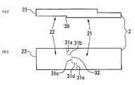
- the boundary line 32 has a stepped shape, and the length in the longitudinal direction of the non-contact portion 22 from the boundary line 32 between the contact portion 21 and the non-contact portion 22 to the free end 23 of the non-contact portion 22.
- the length L1 is formed so as to change stepwise at a position in the width direction orthogonal to the longitudinal direction of the carrier substrate 2. That is, the boundary line 32 between the contact portion 21 and the non-contact portion 22 is a combination of a plurality of straight lines 31a to 31e. Note that each of the plurality of straight lines 31a to 31e may be rounded.
- FIG. 4 is a view of a carrier substrate showing a third specific example of the present invention
- FIG. 4 (a) is a side view
- FIG. 4 (b) is a bottom view.
- the boundary line 33 between the contact portion 21 and the non-contact portion 22 is formed so as to be symmetrical with respect to the width direction of the carrier substrate.
- the plurality of straight lines of the boundary line 33 form a predetermined angle ⁇ of less than 90 degrees with respect to the longitudinal direction of the carrier substrate.
- the intersection of the plurality of straight lines 33a and 33b may be rounded.
- FIG. 5 is a view of a carrier substrate showing a fourth specific example of the present invention
- FIG. 5 (a) is a side view
- FIG. 5 (b) is a bottom view.
- the boundary line 34 between the contact portion 21 and the non-contact portion 22 is a part of a circle, a part of an ellipse, a part of a higher-order function of second or higher order, an arbitrary curve, or a plurality of straight lines. These are formed by a combination of two or more.
- boundary line 34 between the contact portion 21 and the non-contact portion 22 may be formed to be a curve.
- boundary line 34 between the contact portion 21 and the non-contact portion 22 may be a combination of one or more straight lines and one or more curves.
- the boundary line 34 between the contact portion 21 and the non-contact portion 22 may be formed to be bilaterally symmetric with respect to the width direction of the carrier substrate 2.
- the carrier substrate 2 is configured to have a step.
- the carrier substrate 2 may be formed to be flush with the Peltier element 8 and may be configured to have a step on the upper surface side. The same effect can be obtained.
Landscapes
- Physics & Mathematics (AREA)
- Engineering & Computer Science (AREA)
- Condensed Matter Physics & Semiconductors (AREA)
- General Physics & Mathematics (AREA)
- Electromagnetism (AREA)
- Optics & Photonics (AREA)
- General Engineering & Computer Science (AREA)
- Acoustics & Sound (AREA)
- Aviation & Aerospace Engineering (AREA)
- Mechanical Engineering (AREA)
- Semiconductor Lasers (AREA)
- Vibration Prevention Devices (AREA)
Abstract
La présente invention se rapporte à un procédé servant à résoudre un problème tel qu'un composant de structure en porte-à-faux est cassant aux vibrations et aux chocs et, en particulier, un problème tel que les caractéristiques optiques d'un module pour communication optique nécessitant une fiabilité élevée varient au cours du fonctionnement. Dans une structure destinée à supprimer les vibrations d'un élément de support (2), une partie de contact (21) de l'élément de support (2) est fixée à un élément de fixation (8), et une partie de non-contact (22) faisant partie intégrante de la partie de contact (21) est soutenue par l'intermédiaire de la partie de contact (21). L'élément de support (2) est rectangulaire et a une longueur prédéfinie dans le sens longitudinal et une longueur prédéfinie dans le sens de la largeur. La partie de non-contact (22) possède une extrémité libre (23) qui peut vibrer. La longueur longitudinale (L1) de la partie de non-contact depuis la frontière (31) entre la partie de contact et la partie de non-contact jusqu'à l'extrémité libre (23) de la partie de non-contact est différenciée dans une position dans le sens de la largeur croisant le sens longitudinal de façon perpendiculaire.
Applications Claiming Priority (2)
| Application Number | Priority Date | Filing Date | Title |
|---|---|---|---|
| JP2008030740A JP5320762B2 (ja) | 2008-02-12 | 2008-02-12 | 振動抑制構造 |
| JP2008-030740 | 2008-02-12 |
Publications (1)
| Publication Number | Publication Date |
|---|---|
| WO2009101902A1 true WO2009101902A1 (fr) | 2009-08-20 |
Family
ID=40956934
Family Applications (1)
| Application Number | Title | Priority Date | Filing Date |
|---|---|---|---|
| PCT/JP2009/052056 Ceased WO2009101902A1 (fr) | 2008-02-12 | 2009-02-06 | Structure de suppression des vibrations |
Country Status (2)
| Country | Link |
|---|---|
| JP (1) | JP5320762B2 (fr) |
| WO (1) | WO2009101902A1 (fr) |
Families Citing this family (2)
| Publication number | Priority date | Publication date | Assignee | Title |
|---|---|---|---|---|
| JP5544793B2 (ja) * | 2009-09-07 | 2014-07-09 | 富士通株式会社 | 半導体光増幅器モジュール |
| US20180188456A1 (en) | 2015-07-09 | 2018-07-05 | Nec Corporation | Pluggable optical module and optical communication system |
Citations (10)
| Publication number | Priority date | Publication date | Assignee | Title |
|---|---|---|---|---|
| JPS6282761U (fr) * | 1985-11-13 | 1987-05-27 | ||
| JPH05346130A (ja) * | 1992-06-10 | 1993-12-27 | Murata Mfg Co Ltd | 振動吸収バネ |
| JPH06283815A (ja) * | 1993-03-30 | 1994-10-07 | Nippon Steel Corp | 固体レーザ装置 |
| WO1999010882A1 (fr) * | 1997-08-27 | 1999-03-04 | Nhk Spring Co., Ltd. | Dispositif d'actionnement d'objectif |
| JP2000131134A (ja) * | 1998-10-29 | 2000-05-12 | Sumitomo Metal Ind Ltd | 共振子アレイ、音響センサ及び振動センサ |
| JP2001337250A (ja) * | 2000-05-25 | 2001-12-07 | Sumitomo Electric Ind Ltd | 光半導体気密封止容器及び光半導体モジュール |
| US20030099274A1 (en) * | 2001-11-28 | 2003-05-29 | Agere Systems Optoelectronics Guardian Corp. | Laser module |
| JP2006245344A (ja) * | 2005-03-03 | 2006-09-14 | Nec Corp | 波長可変レーザ |
| JP2008028309A (ja) * | 2006-07-25 | 2008-02-07 | Opnext Japan Inc | 光伝送モジュール |
| JP2008193003A (ja) * | 2007-02-07 | 2008-08-21 | Nec Corp | 光モジュール |
-
2008
- 2008-02-12 JP JP2008030740A patent/JP5320762B2/ja not_active Expired - Fee Related
-
2009
- 2009-02-06 WO PCT/JP2009/052056 patent/WO2009101902A1/fr not_active Ceased
Patent Citations (10)
| Publication number | Priority date | Publication date | Assignee | Title |
|---|---|---|---|---|
| JPS6282761U (fr) * | 1985-11-13 | 1987-05-27 | ||
| JPH05346130A (ja) * | 1992-06-10 | 1993-12-27 | Murata Mfg Co Ltd | 振動吸収バネ |
| JPH06283815A (ja) * | 1993-03-30 | 1994-10-07 | Nippon Steel Corp | 固体レーザ装置 |
| WO1999010882A1 (fr) * | 1997-08-27 | 1999-03-04 | Nhk Spring Co., Ltd. | Dispositif d'actionnement d'objectif |
| JP2000131134A (ja) * | 1998-10-29 | 2000-05-12 | Sumitomo Metal Ind Ltd | 共振子アレイ、音響センサ及び振動センサ |
| JP2001337250A (ja) * | 2000-05-25 | 2001-12-07 | Sumitomo Electric Ind Ltd | 光半導体気密封止容器及び光半導体モジュール |
| US20030099274A1 (en) * | 2001-11-28 | 2003-05-29 | Agere Systems Optoelectronics Guardian Corp. | Laser module |
| JP2006245344A (ja) * | 2005-03-03 | 2006-09-14 | Nec Corp | 波長可変レーザ |
| JP2008028309A (ja) * | 2006-07-25 | 2008-02-07 | Opnext Japan Inc | 光伝送モジュール |
| JP2008193003A (ja) * | 2007-02-07 | 2008-08-21 | Nec Corp | 光モジュール |
Also Published As
| Publication number | Publication date |
|---|---|
| JP5320762B2 (ja) | 2013-10-23 |
| JP2009194025A (ja) | 2009-08-27 |
Similar Documents
| Publication | Publication Date | Title |
|---|---|---|
| JP5050548B2 (ja) | 光モジュール | |
| JP5922042B2 (ja) | 光モジュール | |
| JP6872329B2 (ja) | 光ファイバ搭載光集積回路装置 | |
| CN107850732A (zh) | 具有形成在半导体基板上的多模耦合器的光学模块 | |
| US20210364697A1 (en) | Optical module | |
| WO2009101902A1 (fr) | Structure de suppression des vibrations | |
| JP5834461B2 (ja) | 半導体レーザモジュール及びその製造方法 | |
| JP7211236B2 (ja) | 光接続構造 | |
| JP7552083B2 (ja) | 光モジュール | |
| JP4690646B2 (ja) | 温度調節器を有する光学装置およびレーザモジュール | |
| JP2008298912A (ja) | 光学素子及び共振装置 | |
| JP7028362B1 (ja) | 光モジュール | |
| JP5266270B2 (ja) | 光部品 | |
| JP2008197500A (ja) | 光モジュール | |
| JP5458155B2 (ja) | 光受信モジュール | |
| JP2015022018A (ja) | 波長選択スイッチ | |
| US20240192446A1 (en) | Photonic device mechanically isolated from a substrate | |
| JP2014038199A (ja) | 光モジュール | |
| JP2006186462A (ja) | 水晶振動子 | |
| JPWO2009063942A1 (ja) | 光導波路 | |
| CN102362401A (zh) | 半导体激光模块及抑制构件 | |
| JP2010230882A (ja) | 光送信装置 | |
| JP4604204B2 (ja) | 光モジュール | |
| JP5182602B2 (ja) | 可変分散補償器 | |
| JP2004085715A (ja) | 光モジュール |
Legal Events
| Date | Code | Title | Description |
|---|---|---|---|
| 121 | Ep: the epo has been informed by wipo that ep was designated in this application |
Ref document number: 09710891 Country of ref document: EP Kind code of ref document: A1 |
|
| NENP | Non-entry into the national phase |
Ref country code: DE |
|
| 122 | Ep: pct application non-entry in european phase |
Ref document number: 09710891 Country of ref document: EP Kind code of ref document: A1 |