WO2009145461A2 - 세라믹 인쇄회로기판의 원판 및 그 원판의 제조 방법 - Google Patents
세라믹 인쇄회로기판의 원판 및 그 원판의 제조 방법 Download PDFInfo
- Publication number
- WO2009145461A2 WO2009145461A2 PCT/KR2009/001672 KR2009001672W WO2009145461A2 WO 2009145461 A2 WO2009145461 A2 WO 2009145461A2 KR 2009001672 W KR2009001672 W KR 2009001672W WO 2009145461 A2 WO2009145461 A2 WO 2009145461A2
- Authority
- WO
- WIPO (PCT)
- Prior art keywords
- thin film
- printed circuit
- circuit board
- substrate
- depositing
- Prior art date
- Legal status (The legal status is an assumption and is not a legal conclusion. Google has not performed a legal analysis and makes no representation as to the accuracy of the status listed.)
- Ceased
Links
Images

Classifications
-
- H—ELECTRICITY
- H05—ELECTRIC TECHNIQUES NOT OTHERWISE PROVIDED FOR
- H05K—PRINTED CIRCUITS; CASINGS OR CONSTRUCTIONAL DETAILS OF ELECTRIC APPARATUS; MANUFACTURE OF ASSEMBLAGES OF ELECTRICAL COMPONENTS
- H05K1/00—Printed circuits
- H05K1/02—Details
- H05K1/09—Use of materials for the conductive, e.g. metallic pattern
-
- H—ELECTRICITY
- H05—ELECTRIC TECHNIQUES NOT OTHERWISE PROVIDED FOR
- H05K—PRINTED CIRCUITS; CASINGS OR CONSTRUCTIONAL DETAILS OF ELECTRIC APPARATUS; MANUFACTURE OF ASSEMBLAGES OF ELECTRICAL COMPONENTS
- H05K3/00—Apparatus or processes for manufacturing printed circuits
- H05K3/38—Improvement of the adhesion between the insulating substrate and the metal
- H05K3/388—Improvement of the adhesion between the insulating substrate and the metal by the use of a metallic or inorganic thin film adhesion layer
-
- H—ELECTRICITY
- H05—ELECTRIC TECHNIQUES NOT OTHERWISE PROVIDED FOR
- H05K—PRINTED CIRCUITS; CASINGS OR CONSTRUCTIONAL DETAILS OF ELECTRIC APPARATUS; MANUFACTURE OF ASSEMBLAGES OF ELECTRICAL COMPONENTS
- H05K1/00—Printed circuits
- H05K1/02—Details
- H05K1/03—Use of materials for the substrate
- H05K1/0306—Inorganic insulating substrates, e.g. ceramic, glass
-
- H—ELECTRICITY
- H05—ELECTRIC TECHNIQUES NOT OTHERWISE PROVIDED FOR
- H05K—PRINTED CIRCUITS; CASINGS OR CONSTRUCTIONAL DETAILS OF ELECTRIC APPARATUS; MANUFACTURE OF ASSEMBLAGES OF ELECTRICAL COMPONENTS
- H05K2201/00—Indexing scheme relating to printed circuits covered by H05K1/00
- H05K2201/03—Conductive materials
- H05K2201/0302—Properties and characteristics in general
- H05K2201/0317—Thin film conductor layer; Thin film passive component
-
- H—ELECTRICITY
- H05—ELECTRIC TECHNIQUES NOT OTHERWISE PROVIDED FOR
- H05K—PRINTED CIRCUITS; CASINGS OR CONSTRUCTIONAL DETAILS OF ELECTRIC APPARATUS; MANUFACTURE OF ASSEMBLAGES OF ELECTRICAL COMPONENTS
- H05K2201/00—Indexing scheme relating to printed circuits covered by H05K1/00
- H05K2201/03—Conductive materials
- H05K2201/0332—Structure of the conductor
- H05K2201/0335—Layered conductors or foils
- H05K2201/0338—Layered conductor, e.g. layered metal substrate, layered finish layer or layered thin film adhesion layer
-
- H—ELECTRICITY
- H05—ELECTRIC TECHNIQUES NOT OTHERWISE PROVIDED FOR
- H05K—PRINTED CIRCUITS; CASINGS OR CONSTRUCTIONAL DETAILS OF ELECTRIC APPARATUS; MANUFACTURE OF ASSEMBLAGES OF ELECTRICAL COMPONENTS
- H05K3/00—Apparatus or processes for manufacturing printed circuits
- H05K3/10—Apparatus or processes for manufacturing printed circuits in which conductive material is applied to the insulating support in such a manner as to form the desired conductive pattern
- H05K3/14—Apparatus or processes for manufacturing printed circuits in which conductive material is applied to the insulating support in such a manner as to form the desired conductive pattern using spraying techniques to apply the conductive material, e.g. vapour evaporation
- H05K3/16—Apparatus or processes for manufacturing printed circuits in which conductive material is applied to the insulating support in such a manner as to form the desired conductive pattern using spraying techniques to apply the conductive material, e.g. vapour evaporation by cathodic sputtering
-
- H—ELECTRICITY
- H05—ELECTRIC TECHNIQUES NOT OTHERWISE PROVIDED FOR
- H05K—PRINTED CIRCUITS; CASINGS OR CONSTRUCTIONAL DETAILS OF ELECTRIC APPARATUS; MANUFACTURE OF ASSEMBLAGES OF ELECTRICAL COMPONENTS
- H05K3/00—Apparatus or processes for manufacturing printed circuits
- H05K3/46—Manufacturing multilayer circuits
- H05K3/4611—Manufacturing multilayer circuits by laminating two or more circuit boards
- H05K3/4626—Manufacturing multilayer circuits by laminating two or more circuit boards characterised by the insulating layers or materials
- H05K3/4629—Manufacturing multilayer circuits by laminating two or more circuit boards characterised by the insulating layers or materials laminating inorganic sheets comprising printed circuits, e.g. green ceramic sheets
Definitions
- the present invention relates to an original plate of a ceramic printed circuit board and a manufacturing method thereof, and more particularly, to form a high-density electrically conductive layer of a thick film by sputtering for physical vapor deposition on a ceramic substrate, thereby providing excellent heat dissipation characteristics and electrical characteristics. It relates to a master plate of a ceramic printed circuit board having a and a method of manufacturing the master plate.
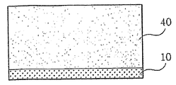
- FIG. 1 is a cross-sectional view of a conventional plate of a ceramic printed circuit board by direct bonding
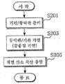
- FIG. 2 is a flowchart illustrating a method of manufacturing a plate of a ceramic printed circuit board by conventional direct bonding.
- the original plate of the ceramic bonded circuit board of the direct bonding method is composed of a ceramic substrate 10 and a copper foil plate 40 directly bonded to the surface of the substrate 10.
- the direct bonding method includes preparing a substrate 10 (S201), heating the substrate 10 and the copper foil plate 40 to a eutectic point of oxygen and copper (S203), and heating the substrate 10. Diffusion of interfacial oxygen to fuse with the copper foil plate 40 to thereby adhere to each other (S205) in order to form the original plate of the printed circuit board.
- This direct bonding method is able to obtain a disc with good adhesion because it is bonded after applying heat to the eutectic point (the eutectic point of oxygen and copper 1065 °C), but due to the heat fusion process, there is a limitation in manufacturing a large area substrate and eutectic There is a limitation in that a thick film must be formed only of a material having a low point. In addition, since a thin plate is used as a material for forming a copper film, there is a problem that it is difficult to manufacture a copper film having a thickness of about 200 micrometers ( ⁇ m) or less.
- a method of depositing a copper thin film using a sputter in a semiconductor manufacturing process may be considered.
- the sputtering method known in the art does not escape the thin film of about nm which can be used for the degree of semiconductor integration, and it has been considered that a thick film of tens to hundreds of micrometers for a printed circuit board is impossible. It was because it had a limit in controlling the stress of the formed film. In order to control the stress, a method of controlling stress by laminating metal layers of different materials has been proposed, but still does not deviate from the level of the thin film.
- An object of the present invention is to form a high density electrical conductive layer of a thick film by sputtering method for physical vapor deposition on a ceramic substrate, and to provide a plate of a ceramic printed circuit board having excellent heat dissipation characteristics and electrical characteristics and a method of manufacturing the disc. In providing.
- the manufacturing method of the original plate of a ceramic printed circuit board having a ceramic substrate for heat dissipation formed on one surface of the electrically conductive layer comprising the steps of preparing the ceramic substrate, physical vapor phase on the ceramic substrate Forming an adhesive layer by a sputtering method for deposition, depositing a first thin film made of a conductive metal and having a compressive residual stress by the sputtering method on the adhesive layer, and sputtering method on the first thin film.
- the first thin film and the second thin film are preferably formed of the same material.
- the adhesive layer is formed of a single film or a multilayer film of at least one material selected from metals, oxides, nitrides, carbides, and polymer resins having excellent heat transfer properties, so that the adhesive layer is physically or chemically bonded to the substrate and the electrically conductive layer. desirable.
- the first thin film is preferably formed in the compressive stress range of -10 GPa to -0.0001 GPa
- the second thin film is formed in the tensile stress range of 0.0001 GPa to 10 GPa.
- the depositing of the first thin film may generate a plasma for sputtering using a DC power supply so that the first thin film has the compressive stress range.
- the DC power supply is preferably controlled so that the energy of the particles sputtered by the plasma is 5 eV or less.
- plasma for sputtering may be generated using a DC pulse power source or an AC power source so that the second thin film has the tensile stress range.
- the DC pulse power source or AC power source is preferably controlled such that the energy of the particles sputtered by the plasma is 5 eV or more and 100 eV or less.
- the first thin film and the second thin film may include copper (Cu), aluminum (Al), silver (Ag), gold (Au), nickel (Ni), platinum (Pt), tungsten (W), or It is preferable that it is any one selected from nickel chromium (NiCr) or an alloy thereof.
- the manufacturing method of the present invention may be formed by depositing a second thin film on the adhesive layer first, and repeatedly depositing the first thin film on the second thin film to form an electrically conductive layer.
- the original plate of a ceramic printed circuit board includes a ceramic substrate, an adhesive layer physically vapor deposited on the ceramic substrate, and an electrically conductive layer physically vapor deposited on the adhesive layer.
- the electrically conductive layer may be formed by alternately repeatedly depositing a first thin film of a conductive metal that is physically vapor deposited and having a compressive residual stress, and a second thin film of a conductive metal that is physically vapor deposited and having a tensile residual stress. Can be.
- the sputtering method in forming a copper thick film on the surface of the substrate, can be used to improve the adhesion between the substrate surface and the metal thick film.
- the residual stress can be controlled within an acceptable range in forming the electrically conductive layer into a thick film. This makes it possible to manufacture a high-density adhesive layer and an electrically conductive layer.
- the adhesive layer is formed by evaporation, unlike the conventional adhesive layer formed of a resin, the adhesion is very excellent, and has excellent heat dissipation characteristics by the high-density adhesive layer.
- Formation of the adhesive layer and the electrically conductive layer by sputtering enables the manufacture of a large-area ceramic printed circuit board, thereby shortening the manufacturing time, thereby improving productivity and reducing the production cost.
- 1 is a cross-sectional view of the original plate of a ceramic printed circuit board by conventional direct bonding
- Figure 2 is a flow chart for explaining the original manufacturing method of a ceramic printed circuit board by direct bonding
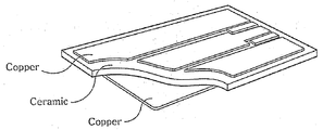
- FIG. 3 is an exploded perspective view of an original plate of a ceramic printed circuit board manufactured by the method of the present invention
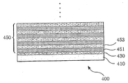
- FIG. 4 is a cross-sectional view of a disc of a ceramic printed circuit board manufactured according to the method of the present invention.
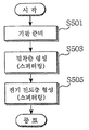
- FIG. 5 is a manufacturing process diagram provided to explain a method for manufacturing a master plate of the ceramic printed circuit board of FIG. 4;
- FIG. 5 is a manufacturing process diagram provided to explain a method for manufacturing a master plate of the ceramic printed circuit board of FIG. 4;
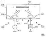
- FIG. 6 is a view schematically showing the structure of a sputter used in the manufacturing process of the present invention
- FIG. 9 is a cross-sectional photograph of a master plate of a ceramic printed circuit board manufactured by the method of the present invention.
- first deposition source 631 first target
- FIG. 3 is an exploded perspective view of an original plate of a ceramic printed circuit board manufactured by the method of the present invention, and is an example of a double-sided substrate on which metal (copper) thick films are formed on both surfaces of the ceramic substrate by the method of the present invention.
- the present invention provides a method of manufacturing a master plate for the ceramic printed circuit board of FIG.
- FIG. 4 is a cross-sectional view of a disc of a ceramic printed circuit board manufactured according to the method of the present invention.
- the original plate 400 of the ceramic printed circuit board manufactured according to the present invention includes a ceramic substrate 410, an adhesive layer 430 formed on the surface of the substrate 410, and an upper surface of the adhesive layer 430. And an electrically conductive layer 450 formed.
- the conductive layer 450 includes a first thin film 451 and a second thin film 453, and will be processed into conductive wires for electrical connection between electrical, electronic or mechanical elements to be mounted on the upper surface after the original fabrication process is completed.
- the first thin film 451 and the second thin film 453 are alternately repeatedly deposited at least once or more to form the conductive layer 450.
- the original plate of the ceramic printed circuit board according to the present invention may also be manufactured as the original plate of the double-sided printed circuit board by forming a second adhesive layer and a second electrically conductive layer on the rear surface of the substrate 410.
- FIG. 5 is a manufacturing process diagram provided to explain the manufacturing method of the original plate of the ceramic printed circuit board of FIG. 4.
- the manufacturing method of the original plate of the ceramic printed circuit board of the present invention will be described with reference to FIG. 5.
- a substrate 410 of a ceramic material is prepared.
- the material of the substrate 410 may be any ceramic material having excellent heat dissipation, but may be aluminum oxide (Al 2 O 3 ), aluminum nitride (AlN), boron nitride (BN), beryllium oxide (BeO), or silicon nitride (Si 3). N 4 ), barium oxide (BaO) and sapphire are preferred.
- the ceramic substrate 410 has excellent durability and heat dissipation characteristics, and thus exhibits excellent performance in dissipating heat generated from mechanical, electrical, or electronic devices mounted on a printed circuit board.
- the adhesive layer 430 is formed on the ceramic substrate 410 by a sputtering method for physical vapor deposition (PVD) of the present invention.
- PVD physical vapor deposition
- the adhesive layer 430 formed by the sputtering method is formed of a material having excellent heat transfer characteristics and adhesion properties, and may be formed of metal, oxide, nitride, carbide, according to the type and chemical characteristics of the substrate 410 and the electrically conductive layer 450. Or various materials such as polymer resin can be used.
- the metal for the adhesive layer 430 is selected from among titanium (Ti), chromium (Cr), nickel (Ni), nichrome (NiCr), aluminum (Al), gold (Au), silver (Ag), and tungsten (W). At least one selected may correspond.
- the oxide may correspond to silicon oxide (SiO X ), titanium oxide (TiO X ), aluminum oxide (Al X O y ), or chromium oxide (CrO X ), and nitride may be silicon nitride (Si X N y ), titanium-based nitride (Ti X N y ), aluminum-based nitride (AlN) or boron-based nitride (BN) may correspond.
- Carbide may be silicon carbide (SiC), titanium carbide (TiC) or chromium carbide (CrC).
- the polymer resin corresponds to a polymer material having excellent heat transfer characteristics and insulation.
- the adhesive layer 430 may be formed of a multilayer of the same material or different materials. In the case of forming a multi-layered film of different materials, the bonding property of the ceramic substrate 410 and the electrically conductive layer 450 to the substrate 410 in the absence of an adhesive layer 430 material having excellent physical or chemical bonding. It is to form a multilayer film of a material having a good bonding property between the good material and the electrically conductive layer 450.
- the thickness of the adhesive layer 430 is preferably considered to have a predetermined withstand voltage characteristic in consideration of the thickness of the ceramic substrate 410, and a thickness of approximately 1 nm to 1 ⁇ m is preferable.
- the sputtering method for forming the adhesive layer 430 may apply a sputtering method for forming the conductive layer 450 to be described below in a corresponding manner.
- the adhesive layer 430 is formed of a multilayer film, the same stress control as the deposition method of the conductive layer 450 will be required.
- the conductive layer 450 may be formed by depositing a predetermined conductive conductor metal on the adhesive layer 430 by a sputtering method.
- the material of the conductive layer 450 is selected from copper (Cu), aluminum (Al), silver (Ag), gold (Au), nickel (Ni), platinum (Pt), tungsten (W) or nickel chromium (NiCr). It may be any one or an alloy thereof, but is not limited thereto and may be a conductive metal. Furthermore, it is preferable to form with the copper (Cu) thick film which used the copper (Cu) as a target among the said metals. In other words, the first thin film 451 and the second thin film 453 may be formed of a conductive metal, and the first thin film 451 and the second thin film 453 may be formed of the same material (eg, copper). .
- the conductive layer 450 is preferably formed of a thick film having a thickness of approximately 5 ⁇ m to 500 ⁇ m, and the thick film is formed by forming the first thin film 451 and the second thin film 453 having a thickness of 1 nm to 10 ⁇ m.
- the present invention solves the problem of the stress caused by conventional thick film formation.
- the first thin film 451 and the second thin film 453 are formed by a sputtering method for physical vapor deposition, and a magnetron sputtering method is preferable.
- sputtering is a widely used method for thin film coating in a semiconductor integrated circuit manufacturing process.
- FIG. 6 is a simplified view showing the structure of the sputter that can be used in the manufacturing process of the present invention, a pump device for vacuum, intake and exhaust means of the inert gas filled in the chamber, cooling means for cooling, and other minor parts It is not shown and description thereof is omitted.
- the sputter 600 includes a first deposition source 630 and a second deposition source 650 provided in the chamber 610.
- the first deposition source 630 includes a first target 631 for the first thin film 451, a DC power supply 633 and a magnetron 635 for supplying DC power to the first target 631.
- the second deposition source 650 may include a second target 651 for the second thin film 453, a DC pulse power supply 653 and a magnetron for supplying a DC pulse to the second target 651. 655).
- the sputter 600 may include a plurality of first deposition sources 630 and second deposition sources 650, and the entire deposition source may be provided in one same chamber 610, or each deposition source. It may have a form separated into separate chambers.
- the chamber 610 is filled with an inert gas such as argon (Ar) to generate a plasma.
- the second deposition source 650 may include an AC power supply device in place of the DC pulse power supply device 653, and supply AC power to the second target 651.
- the DC pulse power supply 653 is provided.
- the magnetrons 635 and 655 form a magnetic field for confining the plasma generated in the chamber 610 in the region near the targets 631 and 651.
- the first target 631 and the second target 651 are preferably formed of the same material, for example, copper.
- Argon (Ar) which is a chemically inert gas, is introduced into the chamber 610, and the DC power supply 633 and the DC pulse power supply 653 sequentially supply power to the first target 631 and the second target 651. Deposition by sputtering takes place while supplying
- argon in the chamber 610 is converted into plasma.
- This plasma is confined to the region near the first target 631 by the magnetic field by the magnetron 635.
- the positively charged argon ions are attracted by the negatively charged first target 631 and collide with each other, and the first target particles are sputtered from the first target 631 by the impact.
- the particles sputtered from the first target 631 are deposited on the adhesive layer 430 of the substrate 410 to form a first thin film 451, which is a film of the first target material.
- the chamber 610 pressure in the sputtering process is preferably about 1 to 10 mTorr.
- the second deposition source 650 operates in conjunction with the movement of the substrate 410 at a predetermined speed and the second thin film 453 is deposited on the first thin film 451 in the same manner.
- the first thin film 451 formed by depositing particles sputtered from the first target 631 by the first deposition source 630 operated by a direct current power source has a characteristic of compressive residual stress.
- the plasma formed by the direct current power source has a lower energy and a smaller ion flux than the plasma generated by the direct current pulse or the alternating current power source, so that the particles sputtered from the first target 631 also have low kinetic energy and ions. You have a ship speed.
- a first thin film 451 having a compressive residual stress is formed.
- the compressive stress can be controlled in the range of approximately -10 GPa to -0.0001 GPa (Giga Pascals).
- the second thin film 453 formed by depositing particles sputtered from the second target 651 by the second deposition source 650 operated by a DC pulse power source has a characteristic of tensile residual stress.
- Plasma formed by the DC pulse power source has a relatively high energy and large ion flux compared to the DC plasma, so that the particles sputtered from the second target 651 also have a high energy and flux.
- Such particles are deposited on the first thin film 451 to form a second thin film 453 having tensile residual stress.
- the tensile stress of the second thin film 453 may be controlled in the range of approximately 0.0001 GPa to 10 GPa.
- Control of the DC pulse power source corresponds to controlling any one of the magnitude, duty cycle, and frequency of the voltage.
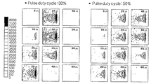
- FIG. 7 is a photograph of the flux of sputtered ion particles at a DC pulse voltage having a different duty cycle, wherein the flux of the sputtered particles generated when the duty cycle of the DC pulse voltage is 30%. It can be seen that it is larger than that of the particles generated with the cycle at 50%. As a result, it can be seen that the flux of the sputtered particles at the DC pulse voltage is much larger than the DC power supply having the duty cycle of 100%.
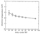
- Figure 8 is a graph measuring the energy of the sputtered particles at the DC pulse voltage having a different duty cycle, it can be seen that the energy of the sputtered particles at the DC pulse voltage is much larger than the DC power supply.
- the control variable of can be obtained experimentally.
- FIG. 9 is a cross-sectional photograph of an original plate of a ceramic printed circuit board manufactured by the method of the present invention, and it can be seen that a thick 150 ⁇ thick conductive film is deposited on an adhesive layer of aluminum oxide (Al 2 O 3 ).
- Equation 2 The residual stress of the conductive layer 450 by the first thin film 451 and the second thin film 453 is expressed by Equation 2 below.
- ⁇ is the total residual stress of the conductive layer 450
- Sc is the compressive stress of the first thin film 451
- St is the tensile stress of the second thin film 453
- n is the first thin film and the second thin film pair It is a number.
- n is 4
- n may vary depending on the thickness of the first thin film 451 and the second thin film 453 itself or the thickness of the entire conductive layer 450. Sc and St may not be the same value.
- the stress ⁇ of the entire conductive layer 450 depends on the characteristics of the thick film, and may be completely canceled out to zero.
- the sputtering apparatus of FIG. 6 is an example in which two deposition sources are disposed, but is not necessarily limited thereto.
- a plurality of deposition sources may be disposed in the chamber 610 and all of the deposition sources may operate simultaneously.
- a plurality of substrates are disposed in the chamber 610 and the deposition process may be simultaneously performed by a plurality of deposition sources while moving at a predetermined speed.
- the thick film may be formed in the order that the second thin film 453 having tensile residual stress is deposited on the adhesive layer 430 first, and then the first thin film 451 having the compressive residual stress is deposited thereon.
- the adhesive layer 430 is also formed in the same manner as the conductive layer 450 is formed. However, the substrate 410 before forming the adhesive layer 430 is used, and the target material is changed.
- the conductive layer 450 Since the film by sputtering is formed at a high density, the conductive layer 450 has excellent electrical and heat transfer characteristics. In addition, the formation of the conductive layer 450 by sputtering forms a large-area film at a high speed, which is suitable for manufacturing a large-area ceramic printed circuit board that can be used for LCD backlight circuits and the like.
- the pattern of the printed circuit to be finally formed on the original plate 400 manufactured by the present invention may be formed using the first thin film 451 and the first thin film by a semiconductor manufacturing process such as a lithography process or an etching process. It may be formed on the two thin films 453. Therefore, the portions of the first thin film 451 and the second thin film 453 which do not form the electric conductors or the pads are removed, and as shown in FIG. 3, a ceramic printed circuit board having a pattern of the electric conductors will be formed. .
Landscapes
- Engineering & Computer Science (AREA)
- Microelectronics & Electronic Packaging (AREA)
- Chemical & Material Sciences (AREA)
- Inorganic Chemistry (AREA)
- Manufacturing & Machinery (AREA)
- Manufacturing Of Printed Wiring (AREA)
- Production Of Multi-Layered Print Wiring Board (AREA)
Abstract
세라믹 인쇄회로기판의 원판 및 그 원판의 제조 방법이 개시된다. 본 발명의 원판 제조방법은, 세라믹 기판 상에 물리적 기상증착을 위한 스퍼터링 방법에 의해 접착층을 형성하는 단계와, 상기 접착층 상에 스퍼터링 방법에 의해 전도성 금속으로 이루어지고 압축 잔류응력을 가지는 제1박막을 증착하는 단계와, 상기 제1박막 상에 스퍼터링 방법에 의해 전도성 금속으로 이루어지고 인장 잔류응력을 가지는 제2박막을 증착하는 단계와, 상기 제1박막 및 제2박막을 증착하는 단계를 반복하여 전체 잔류 응력이 기 설정된 범위내로 제어된 후막의 전기 전도층을 증착하는 단계를 포함한다.
Description
본 발명은 세라믹 인쇄회로기판의 원판 및 그 제조방법에 관한 것으로, 더욱 상세하게는 세라믹 기판 상에 물리적 기상증착을 위한 스퍼터링 방법에 의해 후막의 고밀도 전기 전도층을 형성하여, 뛰어난 방열특성 및 전기적 특성을 가지는 세라믹 인쇄회로기판의 원판 및 그 원판의 제조방법에 관한 것이다.
최근의 전자기기는 집적화와 소형화 추세를 따르고 있다. 전자 기기의 소형화에 따른 여러 가지 문제 중에 하나는 내부 부품에서 발생하는 열의 효과적인 발산이다. 소형화되고 집적화된 전자 기기 내에서는 보다 많은 에너지가 열로 소모되고, 이러한 열은 다시 내부 전자부품의 열화를 일으켜 오동작, 수명 단축 등의 문제를 야기한다.
전자기기 내에서 발생하는 열을 배출하기 위해, 종래로부터 널리 사용되는 방법으로는, 팬(Fan)을 이용한 기기 내의 강제 대류 방법, 열원에 히트 싱크(Heat Sink)를 부착하여 열의 발산을 극대화하는 방법 등이 일반적이었으며, 그 중에서도 최근에 발표되고 있는 세라믹 인쇄회로기판은 전기적 열 발생이 많은 고전압 전력전자 분야, 엘이디(LED) 조명 및 엘시디 백 라이트(LCD Back Light Unit) 등의 분야를 시작으로 주목을 받고 있다.
종래의 세라믹 인쇄회로기판의 원판 제조방법으로 세라믹 기판과 동박판을 직접 접착시키는 방법(DBC: Direct Bonded Copper)이었다. 도 1은 종래의 직접 접착에 의한 세라믹 인쇄회로기판의 원판의 단면도이고, 도 2는 종래의 직접 접착에 의한 세라믹 인쇄회로기판의 원판 제조방법의 설명을 위한 흐름도이다.
도 1을 참조하면, 직접접착방식의 세라믹 인쇄회로기판의 원판은 세라믹 기판(10)과, 기판(10)의 표면에 직접적으로 접착되는 동박(銅薄) 판(40)으로 구성된다.
직접 접착방법은 기판(10)을 준비하는 단계(S201)와, 기판(10)과 동박 판(40)을 산소와 구리의 공융점까지 가열하는 단계(S203)와, 가열된 기판(10)에 계면 산소를 확산시켜 동박 판(40)과 융합시킴으로써 상호 접착시키는 단계(S205)를 순차적으로 진행함으로써 인쇄회로기판의 원판을 형성한다.
이러한 직접접착 방법은 공융점(산소와 구리의 공융점 1065 ℃)까지 열을 가한 후 접착하기 때문에 좋은 접착성을 가진 원판을 획득할 수 있으나 열융착 공정으로 인해 대면적 기판 제작에 한계가 있고 공융점이 낮은 재료로만 후막을 형성해야하는 한계가 있다. 또한, 구리 막을 형성하는 재료로 박판을 이용하기 때문에 약 200 마이크로미터(㎛) 이하의 두께를 갖는 구리막의 제조가 어렵다는 문제점이 있다.
그 밖에도 동막의 형성만을 고려한다면, 반도체 제조 공정상의 스퍼터를 이용하여 동 박막을 증착하는 방법을 고려할 수 있을 것이다. 그러나 종래에 알려진 스퍼터링 방법은 반도체 집적 정도에 사용될 수 ㎚정도의 박막을 벗어나지 못하고 있으며, 인쇄회로기판을 위한 수십 내지 수백 ㎛의 후막은 불가능하다고 여겨져 왔다. 그것은 형성되는 막의 응력을 제어하는데 한계를 가지고 있었기 때문이다. 응력을 제어하기 위해, 서로 다른 소재의 금속층을 적층하는 방법으로 응력 제어를 하는 방법도 제시되었으나, 여전히 박막의 수준을 벗어나지는 못한 것이다.
본 발명의 목적은, 세라믹 기판 상에 물리적 기상증착을 위한 스퍼터링 방법에 의해 후막의 고밀도 전기 전도층을 형성하여, 뛰어난 방열특성 및 전기적 특성을 가지는 세라믹 인쇄회로기판의 원판 및 그 원판의 제조방법을 제공함에 있다.
상기와 같은 목적을 달성하기 위해, 전기 전도층의 일 면에 방열을 위한 세라믹 기판이 형성된 세라믹 인쇄회로기판의 원판의 제조방법은, 상기 세라믹 기판을 준비하는 단계와, 상기 세라믹 기판 상에 물리적 기상증착을 위한 스퍼터링 방법에 의해 접착층을 형성하는 단계와, 상기 접착층 상에 스퍼터링 방법에 의해 전도성 금속으로 이루어지고 압축 잔류응력을 가지는 제1박막을 증착하는 단계와, 상기 제1박막 상에 스퍼터링 방법에 의해 전도성 금속으로 이루어지고 인장 잔류응력을 가지는 제2박막을 증착하는 단계와, 상기 제1박막 및 제2박막을 증착하는 단계를 반복하여 전체 잔류 응력이 기 설정된 범위내로 제어된 후막의 상기 전기 전도층을 증착하는 단계를 포함한다. 제1박막과 제2박막은 동일한 물질로 형성되는 것이 바람직하다.
여기서, 상기 접착층은, 열 전달 특성이 우수한 금속, 산화물, 질화물, 탄화물, 고분자 수지 중에서 선택된 적어도 하나의 물질의 단일막 또는 다층막으로 형성되어, 상기 기판 및 전기 전도층과 물리적 또는 화학적으로 결합하는 것이 바람직하다.
또한, 상기 제1박막은, -10 GPa 내지 -0.0001 GPa의 압축응력범위 내에서 형성되고, 상기 제2박막은 0.0001 GPa 내지 10 GPa의 인장응력범위 내에서 형성되는 것이 바람직하다.
이 경우, 상기 제1박막을 증착하는 단계는 상기 제1박막이 상기 압축응력 범위를 가지도록 스퍼터링을 위한 플라즈마를 직류 전원을 이용하여 생성할 수 있다. 이를 위해, 상기 플라즈마에 의해 스퍼터링된 입자의 에너지가 5 eV 이하가 되도록 상기 직류 전원이 제어되는 것이 바람직하다.
또한, 상기 제2박막을 증착하는 단계는 상기 제2박막이 상기 인장응력 범위를 가지도록 스퍼터링을 위한 플라즈마를 직류 펄스 전원 또는 교류 전원을 이용하여 생성할 수 있다. 이를 위해, 상기 플라즈마에 의해 스퍼터링된 입자의 에너지가 5 eV 이상 100 eV 이하가 되도록 상기 직류 펄스 전원 또는 교류 전원이 제어되는 것이 바람직하다.
실시 예에 따라, 상기 제1박막 및 제2박막은, 구리(Cu), 알루미늄(Al), 은(Ag), 금(Au), 니켈(Ni), 백금(Pt), 텅스텐(W) 또는 니켈크롬(NiCr) 중에서 선택된 어느 하나이거나 그 합금인 것이 바람직하다.
다른 실시 예에 따라, 본 발명의 제조방법은, 상기 접착층 상에 제2박막을 먼저 증착하고, 제2박막에 제1박막을 증착하는 순서로 반복 증착하여 전기 전도층을 형성할 수도 있다.
본 발명의 또 다른 실시 예에 따른 세라믹 인쇄회로기판의 원판은, 세라믹 기판과, 상기 세라믹 기판 상에 물리적으로 기상증착된 접착층과, 상기 접착층 상에 물리적으로 기상증착된 전기 전도층을 포함한다. 여기서, 상기 전기 전도층은, 물리적으로 기상증착되고 압축 잔류응력을 가지는 전도성 금속의 제1박막과 물리적으로 기상증착되고 인장 잔류응력을 가지는 전도성 금속의 제2박막이 교번적으로 반복 증착됨으로써 형성될 수 있다.
본 발명의 세라믹 인쇄회로기판의 원판 제조방법은, 기판의 표면에 동 후막을 형성함에 있어, 스퍼터링 방법을 이용함으로써 기판 표면과 금속 후막 사이의 접착성을 향상시킬 수 있다.
또한, 본 발명의 원판 제조방법은, 전기 전도층을 후막으로 형성함에 있어서, 그 잔류응력을 용인 가능한 범위 내로 제어할 수 있다. 이를 통해, 고밀도의 접착층과 전기 전도층의 제조가 가능해진다.
또한, 접착층은 수지로 형성된 종래의 접착층과 달리 증착에 의해 형성됨으로써 그 접착력이 매우 우수하며, 고밀도의 접착층에 의한 뛰어난 방열특성을 가진다.
스퍼터링에 의한 접착층 및 전기 전도층의 형성은 대면적의 세라믹 인쇄회로기판의 원판 제조를 가능하게 하여 제조 시간을 단축시켜 양산성을 제고하고 이로 인한 생산 단가를 절감할 수 있는 효과가 있다.
도 1은 종래의 직접 접착에 의한 세라믹 인쇄회로기판의 원판의 단면도,
도 2는 종래의 직접 접착에 의한 세라믹 인쇄회로기판의 원판 제조방법의 설명을 위한 흐름도,
도 3은 본 발명의 방법에 의해 제조되는 세라믹 인쇄회로기판의 원판의 분해 사시도,
도 4는 본 발명의 방법에 따라 제조되는 세라믹 인쇄회로기판의 원판의 단면도,
도 5는 도 4의 세라믹 인쇄회로기판의 원판의 제조방법의 설명에 제공되는 제조공정도,
도 6은 본 발명의 제조공정에 사용되는 스퍼터의 구조를 간략히 도시한 도면,
도 7은 서로 다른 듀티 사이클을 가지는 직류 펄스 전압에서의 스퍼터링된 입자를 촬영한 사진,
도 8은 서로 다른 듀티 사이클을 가지는 직류 펄스 전압에서의 스퍼터링된 입자의 에너지를 측정한 그래프, 그리고
도 9는 본 발명의 방법에 의해 제조된 세라믹 인쇄회로기판의 원판의 단면사진이다.
<도면의 주요부분에 대한 부호의 설명>
400: 세라믹 인쇄회로기판의 원판 410: 세라믹 기판
430: 접착층 450: 전기 전도층
451: 제1박막 453: 제2박막
600: 스퍼터 610: 챔버
630: 제1증착원 631: 제1타깃
633: 직류 전원장치 635: 마그네트론
650: 제2증착원 651: 제2타깃
653: 직류 펄스 전원장치(또는 교류 전원장치)
655: 마그네트론
이하 도면을 참조하여 본 발명을 더욱 상세히 설명한다.
도 3은 본 발명의 방법에 의해 제조되는 세라믹 인쇄회로기판의 원판의 분해 사시도로서, 본 발명의 방법에 의해 세라믹 기판의 양면에 금속(구리) 후막이 형성된 양면 기판의 예이다.
본 발명의 방법에 따라, 세라믹 인쇄회로기판의 원판이 제조되면, 다음 공정으로 인쇄회로의 패턴이 도 3과 같이 구리 후막에 형성되어 최종적으로 인쇄회로기판이 될 것이다. 본 발명은 도 3의 세라믹 인쇄회로기판을 위한 원판의 제조방법을 제시한다.
도 4는 본 발명의 방법에 따라 제조되는 세라믹 인쇄회로기판의 원판의 단면도이다.
도 4를 참조하면, 본 발명에 의해 제조되는 세라믹 인쇄회로기판의 원판(400)은 세라믹 기판(410)과, 기판(410)의 표면에 형성된 접착층(430)과, 접착층(430)의 상면에 형성된 전기 전도층(450)을 포함한다. 전도층(450)은 제1박막(451) 및 제2박막(453)을 포함하며, 원판 제조공정이 완료된 후 윗면에 실장될 전기, 전자 또는 기계 소자간의 전기적 연결을 위한 도선으로 가공될 것이다. 제1박막(451) 및 제2박막(453)은 적어도 1회 이상 교번적으로 반복 증착됨으로써 전도층(450)을 형성한다.
또한, 본 발명에 따른 세라믹 인쇄회로기판의 원판은, 기판(410)의 후면에 제2 접착층과 제2 전기 전도층을 형성함으로써 양면 인쇄회로기판의 원판으로도 제조될 수 있다.
도 5는 도 4의 세라믹 인쇄회로기판의 원판의 제조방법의 설명에 제공되는 제조공정도로서, 이하에서는 도 5를 참조하여 본 발명의 세라믹 인쇄회로기판의 원판 제조방법을 설명한다.
<기판 준비, S501 단계>
본 발명의 원판(400) 제조를 위해, 세라믹 소재의 기판(410)이 준비된다. 기판(410)의 재료는 방열 특성이 우수한 세라믹 재료이면 모두 가능할 것이나, 산화알루미늄(Al2O3), 질화알루미늄(AlN), 질화붕소(BN), 산화베릴륨(BeO), 질화실리콘(Si3N4), 산화바륨(BaO) 및 사파이어 중에서 선택되는 것이 바람직하다. 이러한 세라믹 기판(410)은 내구성 및 방열 특성이 우수하여 인쇄회로 기판에 실장된 기계, 전기 또는 전자 소자에서 발생하는 열의 배출에 탁월한 성능을 보인다.
<접착층 형성, S503 단계>
접착층(430)은 본 발명의 물리적기상증착(物理的氣相蒸着, PVD)을 위한 스퍼터링(Sputtering) 방법에 의해 세라믹 기판(410)상에 형성된다. 접착층(430)은 전기 전도층(450)을 세라믹 기판(410)에 접착시킴과 동시에, 전기 전도층(450)에서 발생하는 열을 세라믹 기판(410)으로 전달하는 역할을 한다.
스퍼터링 방법에 의한 접착층(430)은, 열 전달 특성 및 접착성이 우수한 물질로 형성되며, 기판(410)과 전기 전도층(450)의 종류와 그 화학적 특성에 따라 금속, 산화물, 질화물, 탄화물, 또는 고분자 수지 등 다양한 물질이 사용될 수 있다.
여기서, 접착층(430)용 금속은, 티타늄(Ti), 크롬(Cr), 니켈(Ni), 니크롬(NiCr), 알루미늄(Al), 금(Au), 은(Ag) 및 텅스텐(W) 중에서 선택된 적어도 하나가 해당할 수 있다. 산화물은 실리콘 계열 산화물(SiOX), 티타늄 계열 산화물(TiOX), 알루미늄 계열 산화물(AlXOy) 또는 크롬 계열 산화물(CrOX)이 해당할 수 있고, 질화물은 실리콘 계열 질화물(SiXNy), 티타늄 계열 질화물(TiXNy), 알루미늄 계열 질화물(AlN) 또는 붕소 계열 질화물(BN)이 해당할 수 있다. 탄화물은 탄화규소(SiC), 탄화티타늄(TiC) 또는 탄화크롬(CrC)이 해당할 수 있다. 그리고 고분자 수지는 우수한 열전달 특성과, 절연성을 갖는 고분자 물질이 해당한다.
필요에 따라, 접착층(430)은 동일한 물질 또는 서로 다른 물질의 다층 막으로 형성할 수 있다. 서로 다른 물질의 다층 막으로 형성하는 경우는, 세라믹 기판(410)과 전기 전도층(450)에 모두 우수한 물리적 또는 화학적 결합을 가지는 접착층(430) 물질이 없을 경우에 기판(410)과의 결합성이 좋은 물질과 전기 전도층(450)과의 결합성이 좋은 물질의 다층 막을 형성하는 것이다.
접착층(430)의 두께는, 세라믹 기판(410)의 두께를 함께 고려하여 소정의 내전압 특성을 가질 수 있도록 고려되는 것이 바람직하며, 대략 1㎚ ~ 1㎛의 두께가 바람직하다.
접착층(430)을 형성하기 위한 스퍼터링 방법은 아래에서 설명될 전도층(450)의 형성을 위한 스퍼터링 방법을 대응되는 방식으로 적용할 수 있다. 접착층(430)이 다층 막으로 형성될 경우, 전도층(450)의 증착방법과 동일한 응력 제어가 필요할 것이다.
<전기 전도층 형성, S505 단계>
전도층(450)은 소정의 전도성 도전체 금속을 스퍼터링 방법에 의해 접착층(430)에 증착함으로써 형성될 수 있다.
전도층(450)의 소재는 구리(Cu), 알루미늄(Al), 은(Ag), 금(Au), 니켈(Ni), 백금(Pt), 텅스텐(W) 또는 니켈크롬(NiCr) 중에서 선택된 어느 하나이거나 그 합금일 수 있으나 이에 한정되지 아니하며, 전도성 금속이면 가능하다. 나아가, 상기 금속 중에서도 구리(Cu)를 타깃(Target)으로 사용한 구리(Cu) 후막으로 형성되는 것이 바람직하다. 다시 말해, 제1박막(451) 및 제2박막(453)은 전도성 금속으로 형성되며, 제1박막(451)과 제2박막(453)이 동일한 물질(예컨대, 구리)로 형성되는 것이 바람직하다.
전도층(450)은 대략 5㎛ ~ 500㎛의 두께의 후막으로 형성되는 것이 바람직하며, 이러한 두께의 후막 형성은 1 ㎚ 내지 10 ㎛ 두께의 제1박막(451) 및 제2박막(453)을 교번적으로 반복 증착함으로써 전도층(450) 또는 원판(400) 전체의 잔류 응력을 용인 가능한 범위만큼 상쇄시킴으로써 가능하다. 이를 통해, 본 발명은 종래 후막 형성에 따른 응력의 문제를 해소한다.
제1박막(451) 및 제2박막(453)은 물리적기상증착을 위한 스퍼터링 방법에 의해 형성되며, 마그네트론 스퍼터링 방법이 바람직하다.
일반적으로 스퍼터링은 반도체 집적회로 제조 공정에서 박막 코팅을 위해 널리 사용되는 방법이다.
이하에서는 도 6을 참조하여, 본 발명의 접착층 및 전기 전도층의 형성방법을 설명한다. 도 6은 본 발명의 제조공정에 사용될 수 있는 스퍼터의 구조를 간략히 도시한 도면으로서, 진공을 위한 펌프장치, 챔버 내부에 충진하는 불활성 가스의 흡배기 수단, 냉각을 위한 냉각수단, 기타 부수적인 부분은 도시되지 않았으며 그 설명도 생략한다.
도 6을 참조하면, 스퍼터(600)는 챔버(610)에 구비된 제1증착원(630) 및 제2증착원(650)을 포함한다. 제1증착원(630)은 제1박막(451)을 위한 제1타깃(631), 제1타깃(631)에 직류 전원을 공급하기 위한 직류 전원장치(633) 및 마그네트론(635)을 포함한다. 제2증착원(650)은 제2박막(453)을 위한 제2타깃(651), 제2타깃(651)에 직류 펄스(DC Pulse)를 공급하기 위한 직류 펄스 전원장치(653) 및 마그네트론(655)을 포함한다. 스퍼터(600)는 제1증착원(630) 및 제2증착원(650)을 복수 개 포함할 수 있으며, 증착원 전체가 하나의 동일한 챔버(610)내에 마련된 형태를 가질 수도 있고, 각 증착원별로 별개의 챔버로 분리된 형태를 가질 수도 있다. 챔버(610) 내부는 플라즈마를 생성할 불활성 기체, 예컨대 아르곤(Ar) 등이 충진된다.
제2증착원(650)은 직류 펄스 전원장치(653)를 대신하여 교류 전원장치를 포함하고, 제2타깃(651)에 교류 전원을 공급할 수 있다. 다만, 이하에서는 직류 펄스 전원장치(653)가 마련된 경우를 중심으로 설명한다.
마그네트론(635, 655)은 챔버(610) 내에서 생성되는 플라즈마를 타깃(631, 651) 부근 영역 안에 구속하기 위한 자계를 형성시킨다. 앞서 설명한 바와 같이, 제1타깃(631) 및 제2 타깃(651)은 동일한 물질, 예컨대 구리로 형성되는 것이 바람직하다.
화학적으로 불활성 가스인 아르곤(Ar)이 챔버(610) 내로 유입되고, 직류 전원장치(633)와 직류 펄스 전원장치(653)가 순차적으로 제1타깃(631) 및 제2타깃(651)에 전원을 공급하면서 스퍼터링에 의한 증착이 이루어진다.
직류 전원장치(633)가 동작하면, 챔버(610) 내의 아르곤이 플라즈마화 한다. 이 플라즈마는 마그네트론(635)에 의한 자계에 의하여 제1타깃(631) 부근의 영역으로 구속된다. 양으로 대전된 아르곤 이온들은 음으로 대전된 제1타깃(631)에 의해 끌어당겨져 충돌하게 되고, 그 충격에 의해 제1타깃 입자들이 제1타깃(631)으로부터 스퍼터링 된다. 제1타깃(631)으로부터 스퍼터링된 입자들은 기판(410)의 접착층(430)에 증착됨으로써 제1타깃 물질의 막인 제1박막(451)이 형성된다. 이 경우, 스퍼터링 공정상의 챔버(610) 압력은 약 1 ~ 10 mTorr가 바람직하다.
동일한 압력조건에서, 기판(410)이 소정의 속도로 이동하는 것과 연계하여 제2증착원(650)이 동작하고 동일한 방법으로 제2박막(453)이 제1박막(451)위에 증착된다.
직류 전원에 의해 동작하는 제1증착원(630)에 의해 제1타깃(631)으로부터 스퍼링된 입자가 증착하여 형성되는 제1박막(451)은, 압축 잔류 응력의 특성을 갖게 된다.
직류 전원에 의해 형성되는 플라즈마는 직류 펄스 또는 교류 전원에 의한 플라즈마보다 상대적으로 낮은 에너지 및 작은 이온 선속(線束, Flux)을 가지게 됨으로써, 제1타깃(631)으로부터 스퍼터링된 입자도 낮은 운동 에너지와 이온 선속을 가지게 된다. 이런 낮은 에너지 입자가 접착층(430)에 증착되면, 압축 잔류 응력을 갖는 제1박막(451)이 형성된다. 압축 응력은 대략 -10 GPa 내지 -0.0001 GPa(기가 파스칼)의 범위 내에서 제어될 수 있다. 이를 위해, 직류 플라즈마에 의해 스퍼터링된 입자의 에너지 E가 5 eV 미만이도록 직류 전원장치의 직류 전원을 제어하는 것이 바람직하다.
직류 펄스 전원에 의해 동작하는 제2증착원(650)에 의해 제2타깃(651)으로부터 스퍼링된 입자가 증착하여 형성되는 제2박막(453)은, 인장 잔류 응력의 특성을 갖게 된다.
직류 펄스 전원에 의해 형성되는 플라즈마는 직류 플라즈마에 비해 상대적으로 높은 에너지 및 큰 이온 선속을 가지게 됨으로써, 제2타깃(651)으로부터 스퍼터링된 입자도 높은 에너지와 선속을 가지게 된다. 이런 입자가 제1박막(451)에 증착되면서 인장 잔류 응력을 갖는 제2박막(453)을 형성하게 된다. 제2박막(453)이 가지는 인장 응력은 대략 0.0001 GPa 내지 10 GPa 의 범위 내에서 제어될 수 있다. 이를 위해, 직류 펄스(또는 교류) 플라즈마에 의해 스퍼터링된 입자의 에너지 E가 다음의 수학식 1을 만족하도록, 직류 펄스(또는 교류) 전원장치의 직류 펄스(또는 교류) 전원을 제어하는 것이 바람직하다.
수학식 1 
직류 펄스 전원의 제어는 그 전압의 크기, 듀티 사이클, 주파수 중 어느 하나를 제어하는 것에 해당한다.
도 7은 서로 다른 듀티 사이클을 가지는 직류 펄스 전압에서의 스퍼터링된 이온 입자의 선속을 촬영한 사진으로서, 직류 펄스 전압의 듀티 사이클(Duty Cycle)이 30 %인 상태에서 발생한 스퍼터링된 입자의 선속이 듀티 사이클이 50 %인 상태에서 발생한 입자의 그것보다 큼을 알 수 있다. 결국, 듀티 사이클이 100%가 되는 직류 전원보다 직류 펄스 전압에서의 스퍼터링된 입자의 선속이 훨씬 큼을 알 수 있다. 마찬가지로, 도 8은 서로 다른 듀티 사이클을 가지는 직류 펄스 전압에서의 스퍼터링된 입자의 에너지를 측정한 그래프로서, 직류 전원보다 직류 펄스 전압에서의 스퍼터링된 입자의 에너지가 훨씬 큼을 알 수 있다. 따라서 서로 대비되어 상쇄되는 제1박막(451)의 압축 잔류응력 값과 제2박막(453)의 인장 잔류응력 값, 또는 그 응력 값을 위한 직류 전원장치(633) 및 직류 펄스 전원장치(653)의 제어변수는 실험적으로 구해질 수 있다.
제1박막(451)의 압축 잔류응력은 제2박막(453)의 인장 잔류응력에 의해 전체 또는 일부 상쇄된다. 이러한 제1박막(451)과 제2박막(453)은 그 응력이 서로 상쇄되도록 교번적으로 반복 형성됨으로써, 그 응력이 전체적으로 제어되는 후막의 전도층(450)이 형성된다. 도 9는 본 발명의 방법에 의해 제조된 세라믹 인쇄회로기판의 원판의 단면사진으로서, 산화알루미늄(Al2O3)의 접착층 위에 150 ㎛ 두께의 고밀도 전도층 후막이 증착되어 있음을 알 수 있다.
제1박막(451)과 제2박막(453)에 의한 전도층(450)의 잔류응력은 다음의 수학식 2와 같다.
수학식 2 
여기서, σ는 전도층(450)의 총 잔류응력, Sc는 제1박막(451)의 압축응력, St는 제2박막(453)의 인장응력, 그리고 n은 제1박막과 제2박막 쌍의 수이다. 도 4의 원판(400)은 n이 4인 경우로서, 제1박막(451)과 제2박막(453)이 4번 반복 증착됨을 알 수 있다. 동일한 두께의 전도층(450)이라도 제1박막(451) 및 제2박막(453) 자체의 두께 또는 전체 전도층(450)의 두께에 따라, n은 달라질 수 있다. Sc와 St도 동일한 값이 아닐 수 있다.
전도층(450) 전체의 응력 σ은 후막의 특성에 따라 달라지며, 완전히 상쇄되어 0이 될 수도 있다.
도 6의 스퍼터 장치는 두 개의 증착원을 배치한 예이나 반드시 이에 한정되는 것은 아니다. 예컨대, 챔버(610)에는 복수 개의 증착원이 배치되고 전체 증착원이 동시에 동작할 수 있다. 이때, 챔버(610)에는 복수 개의 기판이 배치되고 소정 속도로 이동하면서 복수 개의 증착원에 의해 동시에 증착과정이 진행될 수도 있다.
실시 예에 따라, 접착층(430)에 인장 잔류응력을 가지는 제2박막(453)이 먼저 증착되고 그 위에 압축 잔류응력을 가지는 제1박막(451)이 증착되는 순서로 후막이 형성될 수도 있다.
접착층(430)도 전도층(450)의 형성과 동일한 방법으로 이루어진다. 다만, 접착층(430)을 형성하기 이전의 기판(410)이 사용되고 타깃 물질이 달라지는 것이다.
스퍼터링에 의한 막은 고밀도로 형성되기 때문에, 전도층(450)은 우수한 전기적 특성 및 열전달 특성을 가진다. 또한, 스퍼터링에 의한 전도층(450)의 형성은 고속으로 대면적의 막을 형성함으로써, 엘시디 백라이트 회로 등에 사용될 수 있는 대면적 세라믹 인쇄회로기판의 제조에도 적합하다.
본 발명에 의해 제조된 원판(400)상에 최종적으로 형성될 인쇄회로의 패턴(Pattern)은 사진공정(Lithograph), 식각공정(Etching) 등의 반도체 제조공정에 의해 제1박막(451) 및 제2박막(453)에 형성될 수 있다. 따라서 제1박막(451) 및 제2박막(453) 중 전기적 도선 또는 패드(Pad)를 형성하지 아니하는 부분은 제거되고, 도 3과 같이 전기 도선의 패턴이 형성된 세라믹 인쇄회로기판이 형성될 것이다.
이상에서는 본 발명의 바람직한 실시 예에 대하여 도시하고 설명하였지만, 본 발명은 상술한 특정의 실시 예에 한정되지 아니하며, 청구범위에서 청구하는 본 발명의 요지를 벗어남이 없이 당해 발명이 속하는 기술 분야에서 통상의 지식을 가진 자에 의해 다양한 변형실시가 가능한 것은 물론이고, 이러한 변형실시들은 본 발명의 기술적 사상이나 전망으로부터 개별적으로 이해되어서는 안 될 것이다.
Claims (13)
- 전기 전도층의 일 면에 방열을 위한 세라믹 기판이 형성된 세라믹 인쇄회로기판의 원판의 제조방법에 있어서,상기 세라믹 기판을 준비하는 단계;상기 세라믹 기판 상에 물리적 기상증착을 위한 스퍼터링 방법에 의해 접착층을 형성하는 단계;상기 접착층 상에 스퍼터링 방법에 의해 전도성 금속으로 이루어지고 압축 잔류응력을 가지는 제1박막을 증착하는 단계;상기 제1박막 상에 스퍼터링 방법에 의해 전도성 금속으로 이루어지고 인장 잔류응력을 가지는 제2박막을 증착하는 단계; 및상기 제1박막 및 제2박막을 증착하는 단계를 반복하여 전체 잔류 응력이 기 설정된 범위내로 제어된 후막의 상기 전기 전도층을 증착하는 단계를 포함하는 것을 특징으로 하는 세라믹 인쇄회로기판의 원판 제조방법.
- 전기 전도층의 일 면에 방열을 위한 세라믹 기판이 형성된 세라믹 인쇄회로기판의 원판의 제조방법에 있어서,세라믹 기판을 준비하는 단계;상기 세라믹 기판 상에 물리적 기상증착을 위한 스퍼터링 방법에 의해 접착층을 형성하는 단계;상기 접착층 상에 스퍼터링 방법에 의해 전도성 금속으로 이루어지고 인장 잔류응력을 가지는 제2박막을 증착하는 단계;상기 제2박막 상에 스퍼터링 방법에 의해 전도성 금속으로 이루어지고 압축 잔류응력을 가지는 제1박막을 증착하는 단계; 및상기 제2박막 및 제1박막을 증착하는 단계를 반복하여 전체 잔류 응력이 기 설정된 범위내로 제어된 후막의 전기 전도층을 증착하는 단계를 포함하는 것을 특징으로 하는 세라믹 인쇄회로기판의 원판 제조방법.
- 제1항 또는 제2항에 있어서,상기 접착층은, 열 전달 특성이 우수한 금속, 산화물, 질화물, 탄화물, 고분자 수지 중에서 선택된 적어도 하나의 물질의 단일막 또는 다층막으로 형성되어 상기 기판 및 전기 전도층과 물리적 또는 화학적으로 결합하는 것을 특징으로 하는 세라믹 인쇄회로기판의 원판 제조방법.
- 제1항 또는 제2항에 있어서,상기 제1박막 및 제2박막은, 구리(Cu), 알루미늄(Al), 은(Ag), 금(Au), 니켈(Ni), 백금(Pt), 텅스텐(W) 또는 니켈크롬(NiCr) 중에서 선택된 어느 하나이거나 그 합금인 것을 특징으로 하는 세라믹 인쇄회로기판의 원판 제조방법.
- 제1항 또는 제2항에 있어서,상기 제1박막은, -10 GPa 내지 -0.0001 GPa의 압축응력범위 내에서 형성되고,상기 제2박막은 0.0001 GPa 내지 10 GPa의 인장응력범위 내에서 형성되는 것을 특징으로 하는 세라믹 인쇄회로기판의 원판 제조방법.
- 제5항에 있어서,상기 제1박막을 증착하는 단계는 상기 제1박막이 상기 압축응력 범위를 가지도록, 스퍼터링을 위한 플라즈마를 직류 전원을 이용하여 생성하는 것을 특징으로 하는 세라믹 인쇄회로기판의 원판 제조방법.
- 제6항에 있어서,상기 플라즈마에 의해 스퍼터링된 입자의 에너지가 5 eV 이하가 되도록 상기 직류 전원이 제어되는 것을 특징으로 하는 세라믹 인쇄회로기판의 원판 제조방법.
- 제5항에 있어서,상기 제2박막을 증착하는 단계는 상기 제2박막이 상기 인장응력 범위를 가지도록, 스퍼터링을 위한 플라즈마를 직류 펄스 전원 또는 교류 전원을 이용하여 생성하는 것을 특징으로 하는 세라믹 인쇄회로기판의 원판 제조방법.
- 제8항에 있어서,상기 플라즈마에 의해 스퍼터링된 입자의 에너지가 5 eV 이상 100 eV 이하가 되도록 상기 직류 펄스 전원 또는 교류 전원이 제어되는 것을 특징으로 하는 세라믹 인쇄회로기판의 원판 제조방법.
- 세라믹 기판;상기 세라믹 기판 상에 물리적으로 기상증착된 접착층; 및상기 접착층 상에 물리적으로 기상증착된 전기 전도층;을 포함하고,상기 전기 전도층은,물리적으로 기상증착되고 압축 잔류응력을 가지는 전도성 금속의 제1박막; 및물리적으로 기상증착되고 인장 잔류응력을 가지는 전도성 금속의 제2박막;이 교번적으로 반복 증착된 것임을 특징으로 하는 세라믹 인쇄회로기판의 원판.
- 제10항에 있어서,상기 접착층은, 열 전달 특성이 우수한 금속, 산화물, 질화물, 탄화물, 고분자 수지 중에서 선택된 적어도 하나의 물질의 단일막 또는 다층막으로 형성되어 상기 기판 및 전기 전도층과 화학적으로 결합한 것임을 특징으로 하는 세라믹 인쇄회로기판의 원판.
- 제10항에 있어서,상기 제1박막 및 제2박막은, 구리(Cu), 알루미늄(Al), 은(Ag), 금(Au), 니켈(Ni), 백금(Pt), 텅스텐(W) 또는 니켈크롬(NiCr) 중에서 선택된 어느 하나이거나 그 합금인 것을 특징으로 하는 세라믹 인쇄회로기판의 원판.
- 제10항에 있어서,상기 제1박막은, -10 GPa 내지 -0.0001 GPa의 압축응력범위 내에서 형성되고,상기 제2박막은 0.0001 GPa 내지 10 GPa의 인장응력범위 내에서 형성되는 것을 특징으로 하는 세라믹 인쇄회로기판의 원판.
Applications Claiming Priority (4)
| Application Number | Priority Date | Filing Date | Title |
|---|---|---|---|
| KR10-2008-0031268 | 2008-04-03 | ||
| KR1020080031268A KR100885664B1 (ko) | 2008-04-03 | 2008-04-03 | 고속/고밀도 마그네트론 스퍼터링 법을 이용한 후막제조방법 |
| KR10-2008-0031284 | 2008-04-03 | ||
| KR1020080031284A KR100867756B1 (ko) | 2008-04-03 | 2008-04-03 | 고속/고밀도 마그네트론 스퍼터링 법을 이용한 세라믹인쇄회로기판의 원판 제조 방법 |
Publications (2)
| Publication Number | Publication Date |
|---|---|
| WO2009145461A2 true WO2009145461A2 (ko) | 2009-12-03 |
| WO2009145461A3 WO2009145461A3 (ko) | 2010-01-21 |
Family
ID=41313620
Family Applications (1)
| Application Number | Title | Priority Date | Filing Date |
|---|---|---|---|
| PCT/KR2009/001672 Ceased WO2009145461A2 (ko) | 2008-04-03 | 2009-04-01 | 세라믹 인쇄회로기판의 원판 및 그 원판의 제조 방법 |
Country Status (2)
| Country | Link |
|---|---|
| JP (1) | JP2009253275A (ko) |
| WO (1) | WO2009145461A2 (ko) |
Cited By (6)
| Publication number | Priority date | Publication date | Assignee | Title |
|---|---|---|---|---|
| CN113174575A (zh) * | 2021-03-31 | 2021-07-27 | 西安交通大学 | 一种AlN陶瓷基板金属化、热沉一体化制备方法 |
| WO2023201618A1 (zh) * | 2022-04-21 | 2023-10-26 | 京东方科技集团股份有限公司 | 线路板、发光基板、背光模组、显示面板及显示装置 |
| NO347559B1 (en) * | 2022-06-21 | 2024-01-15 | Univ Of South Eastern Norway | Process for producing single crystal silver films |
| US12457685B2 (en) | 2022-10-31 | 2025-10-28 | Beijing Boe Technology Development Co., Ltd. | Circuit board, light-emitting substrate, backlight module, and display apparatus |
| US12563875B2 (en) | 2021-12-29 | 2026-02-24 | Boe Technology Group Co., Ltd. | Wiring board, functional backplane, backlight module, display panel and display apparatus |
| US12581596B2 (en) | 2021-12-31 | 2026-03-17 | Boe Technology Group Co., Ltd. | Wiring board, functional backplane and method for manufacturing the same |
Families Citing this family (3)
| Publication number | Priority date | Publication date | Assignee | Title |
|---|---|---|---|---|
| JP2024523448A (ja) * | 2021-06-25 | 2024-06-28 | コーニング インコーポレイテッド | ガラス含有基板上に金属層を形成する方法および結果として得られるデバイス |
| CN116965159A (zh) | 2022-02-24 | 2023-10-27 | 京东方科技集团股份有限公司 | 线路板及其制造方法、功能背板、背光模组、显示装置 |
| TWI898203B (zh) * | 2022-04-21 | 2025-09-21 | 中國商京東方科技集團股份有限公司 | 電路板、發光基板、背光模組、顯示面板及顯示裝置 |
Family Cites Families (10)
| Publication number | Priority date | Publication date | Assignee | Title |
|---|---|---|---|---|
| JPH07161637A (ja) * | 1988-01-26 | 1995-06-23 | Toshiba Corp | 膜のスパッタリング形成方法 |
| JPH0775124B2 (ja) * | 1990-01-25 | 1995-08-09 | 工業技術院長 | 薄膜の堆積方法 |
| KR950006415B1 (ko) * | 1993-06-11 | 1995-06-15 | 주식회사에스.케이.씨 | 광자기기록매체의 제조방법 |
| JP3226816B2 (ja) * | 1996-12-25 | 2001-11-05 | キヤノン販売株式会社 | 層間絶縁膜の形成方法、半導体装置及びその製造方法 |
| JP2002111176A (ja) * | 2000-09-26 | 2002-04-12 | Rohm Co Ltd | 導電路の形成方法および基板 |
| JP2004087913A (ja) * | 2002-08-28 | 2004-03-18 | Yamaha Corp | 銅メッキセラミックス基板およびその製造方法ならびに銅メッキセラミックス基板を備えた熱電モジュール |
| JP2005298833A (ja) * | 2002-10-22 | 2005-10-27 | Asahi Glass Co Ltd | 多層膜付き基板とその製造方法 |
| KR100688823B1 (ko) * | 2004-07-21 | 2007-03-02 | 삼성전기주식회사 | 고밀도 기판의 제조방법 |
| JP2006286971A (ja) * | 2005-03-31 | 2006-10-19 | Tdk Corp | 複合基板およびその製造方法、ならびに薄膜デバイスおよびその製造方法 |
| JP2007234397A (ja) * | 2006-03-01 | 2007-09-13 | Ulvac Japan Ltd | 透明電極及びその形成方法 |
-
2009
- 2009-01-07 JP JP2009001554A patent/JP2009253275A/ja active Pending
- 2009-04-01 WO PCT/KR2009/001672 patent/WO2009145461A2/ko not_active Ceased
Cited By (7)
| Publication number | Priority date | Publication date | Assignee | Title |
|---|---|---|---|---|
| CN113174575A (zh) * | 2021-03-31 | 2021-07-27 | 西安交通大学 | 一种AlN陶瓷基板金属化、热沉一体化制备方法 |
| US12563875B2 (en) | 2021-12-29 | 2026-02-24 | Boe Technology Group Co., Ltd. | Wiring board, functional backplane, backlight module, display panel and display apparatus |
| US12581596B2 (en) | 2021-12-31 | 2026-03-17 | Boe Technology Group Co., Ltd. | Wiring board, functional backplane and method for manufacturing the same |
| WO2023201618A1 (zh) * | 2022-04-21 | 2023-10-26 | 京东方科技集团股份有限公司 | 线路板、发光基板、背光模组、显示面板及显示装置 |
| US12610675B2 (en) | 2022-04-21 | 2026-04-21 | Boe Technology Group Co., Ltd. | Circuit board, light-emitting substrate, backlight module, display panel and display device |
| NO347559B1 (en) * | 2022-06-21 | 2024-01-15 | Univ Of South Eastern Norway | Process for producing single crystal silver films |
| US12457685B2 (en) | 2022-10-31 | 2025-10-28 | Beijing Boe Technology Development Co., Ltd. | Circuit board, light-emitting substrate, backlight module, and display apparatus |
Also Published As
| Publication number | Publication date |
|---|---|
| JP2009253275A (ja) | 2009-10-29 |
| WO2009145461A3 (ko) | 2010-01-21 |
Similar Documents
| Publication | Publication Date | Title |
|---|---|---|
| WO2009145461A2 (ko) | 세라믹 인쇄회로기판의 원판 및 그 원판의 제조 방법 | |
| WO2009145492A2 (ko) | 마그네트론 스퍼터링에 의한 후막제조방법 | |
| WO2009145462A2 (ko) | 금속 인쇄회로기판의 원판 및 그 원판의 제조 방법 | |
| US10535545B2 (en) | Substrate fixing device | |
| US6166897A (en) | Static chuck apparatus and its manufacture | |
| KR100985849B1 (ko) | 세라믹 인쇄회로기판의 원판 및 그 제조방법 | |
| KR101096114B1 (ko) | 일체형 전력 반도체 모듈 기판의 제조방법 | |
| CN1142169A (zh) | 电路板卡及其制造方法 | |
| KR100867756B1 (ko) | 고속/고밀도 마그네트론 스퍼터링 법을 이용한 세라믹인쇄회로기판의 원판 제조 방법 | |
| KR101075147B1 (ko) | 금속 인쇄회로기판의 원판 및 그 제조방법 | |
| WO2017014343A1 (ko) | 신축성이 향상된 메타 계면 구조물 및 그 제조방법 | |
| CN1376308A (zh) | 溅射方法 | |
| JP7701149B2 (ja) | 静電チャックの製造方法 | |
| KR101116516B1 (ko) | 열적 특성이 개선된 전력 반도체 모듈용 메탈라이징 세라믹 기판 및 그 제조방법 | |
| JP2001077185A (ja) | 静電チャック及びその製造方法 | |
| KR101062843B1 (ko) | 금속 인쇄회로기판의 원판 및 그 제조방법 | |
| TW202445743A (zh) | 基板固定裝置 | |
| WO2017065407A1 (ko) | 세라믹 회로기판 및 이의 제조방법 | |
| WO2017069398A1 (ko) | 세라믹 회로기판 및 이의 제조방법 | |
| KR102852232B1 (ko) | 정전 척 및 기판 고정 장치 | |
| JPH0575255A (ja) | 混成基板とこれを搭載する回路モジユールおよびその製造方法 | |
| JP2005033068A (ja) | 高周波回路用基板の製造方法及び高周波電子装置 | |
| CN1292626C (zh) | 一种电路板及其制造方法 | |
| WO2017122966A1 (ko) | 세라믹 회로기판 및 이의 제조방법 | |
| CN2588504Y (zh) | 微型低电压低阻值电流感测器 |
Legal Events
| Date | Code | Title | Description |
|---|---|---|---|
| 121 | Ep: the epo has been informed by wipo that ep was designated in this application |
Ref document number: 09754926 Country of ref document: EP Kind code of ref document: A2 |
|
| NENP | Non-entry into the national phase |
Ref country code: DE |
|
| 122 | Ep: pct application non-entry in european phase |
Ref document number: 09754926 Country of ref document: EP Kind code of ref document: A2 |