WO2009147828A1 - Procédé de production d’un dispositif à semi-conducteur et dispositif à semi-conducteur - Google Patents
Procédé de production d’un dispositif à semi-conducteur et dispositif à semi-conducteur Download PDFInfo
- Publication number
- WO2009147828A1 WO2009147828A1 PCT/JP2009/002447 JP2009002447W WO2009147828A1 WO 2009147828 A1 WO2009147828 A1 WO 2009147828A1 JP 2009002447 W JP2009002447 W JP 2009002447W WO 2009147828 A1 WO2009147828 A1 WO 2009147828A1
- Authority
- WO
- WIPO (PCT)
- Prior art keywords
- semiconductor device
- manufacturing
- thermosetting resin
- resin composition
- paste
- Prior art date
- Legal status (The legal status is an assumption and is not a legal conclusion. Google has not performed a legal analysis and makes no representation as to the accuracy of the status listed.)
- Ceased
Links
Images
Classifications
-
- H—ELECTRICITY
- H10—SEMICONDUCTOR DEVICES; ELECTRIC SOLID-STATE DEVICES NOT OTHERWISE PROVIDED FOR
- H10W—GENERIC PACKAGES, INTERCONNECTIONS, CONNECTORS OR OTHER CONSTRUCTIONAL DETAILS OF DEVICES COVERED BY CLASS H10
- H10W72/00—Interconnections or connectors in packages
- H10W72/01—Manufacture or treatment
- H10W72/013—Manufacture or treatment of die-attach connectors
-
- C—CHEMISTRY; METALLURGY
- C09—DYES; PAINTS; POLISHES; NATURAL RESINS; ADHESIVES; COMPOSITIONS NOT OTHERWISE PROVIDED FOR; APPLICATIONS OF MATERIALS NOT OTHERWISE PROVIDED FOR
- C09D—COATING COMPOSITIONS, e.g. PAINTS, VARNISHES OR LACQUERS; FILLING PASTES; CHEMICAL PAINT OR INK REMOVERS; INKS; CORRECTING FLUIDS; WOODSTAINS; PASTES OR SOLIDS FOR COLOURING OR PRINTING; USE OF MATERIALS THEREFOR
- C09D163/00—Coating compositions based on epoxy resins; Coating compositions based on derivatives of epoxy resins
-
- H—ELECTRICITY
- H10—SEMICONDUCTOR DEVICES; ELECTRIC SOLID-STATE DEVICES NOT OTHERWISE PROVIDED FOR
- H10W—GENERIC PACKAGES, INTERCONNECTIONS, CONNECTORS OR OTHER CONSTRUCTIONAL DETAILS OF DEVICES COVERED BY CLASS H10
- H10W74/00—Encapsulations, e.g. protective coatings
- H10W74/01—Manufacture or treatment
- H10W74/012—Manufacture or treatment of encapsulations on active surfaces of flip-chip devices, e.g. forming underfills
-
- H—ELECTRICITY
- H10—SEMICONDUCTOR DEVICES; ELECTRIC SOLID-STATE DEVICES NOT OTHERWISE PROVIDED FOR
- H10W—GENERIC PACKAGES, INTERCONNECTIONS, CONNECTORS OR OTHER CONSTRUCTIONAL DETAILS OF DEVICES COVERED BY CLASS H10
- H10W74/00—Encapsulations, e.g. protective coatings
- H10W74/10—Encapsulations, e.g. protective coatings characterised by their shape or disposition
- H10W74/15—Encapsulations, e.g. protective coatings characterised by their shape or disposition on active surfaces of flip-chip devices, e.g. underfills
-
- H—ELECTRICITY
- H10—SEMICONDUCTOR DEVICES; ELECTRIC SOLID-STATE DEVICES NOT OTHERWISE PROVIDED FOR
- H10W—GENERIC PACKAGES, INTERCONNECTIONS, CONNECTORS OR OTHER CONSTRUCTIONAL DETAILS OF DEVICES COVERED BY CLASS H10
- H10W74/00—Encapsulations, e.g. protective coatings
- H10W74/40—Encapsulations, e.g. protective coatings characterised by their materials
- H10W74/47—Encapsulations, e.g. protective coatings characterised by their materials comprising organic materials, e.g. plastics or resins
-
- H—ELECTRICITY
- H05—ELECTRIC TECHNIQUES NOT OTHERWISE PROVIDED FOR
- H05K—PRINTED CIRCUITS; CASINGS OR CONSTRUCTIONAL DETAILS OF ELECTRIC APPARATUS; MANUFACTURE OF ASSEMBLAGES OF ELECTRICAL COMPONENTS
- H05K1/00—Printed circuits
- H05K1/02—Details
- H05K1/0271—Arrangements for reducing stress or warp in rigid printed circuit boards, e.g. caused by loads, vibrations or differences in thermal expansion
-
- H—ELECTRICITY
- H05—ELECTRIC TECHNIQUES NOT OTHERWISE PROVIDED FOR
- H05K—PRINTED CIRCUITS; CASINGS OR CONSTRUCTIONAL DETAILS OF ELECTRIC APPARATUS; MANUFACTURE OF ASSEMBLAGES OF ELECTRICAL COMPONENTS
- H05K1/00—Printed circuits
- H05K1/02—Details
- H05K1/03—Use of materials for the substrate
- H05K1/0313—Organic insulating material
- H05K1/0353—Organic insulating material consisting of two or more materials, e.g. two or more polymers, polymer + filler, + reinforcement
- H05K1/0373—Organic insulating material consisting of two or more materials, e.g. two or more polymers, polymer + filler, + reinforcement containing additives, e.g. fillers
-
- H—ELECTRICITY
- H05—ELECTRIC TECHNIQUES NOT OTHERWISE PROVIDED FOR
- H05K—PRINTED CIRCUITS; CASINGS OR CONSTRUCTIONAL DETAILS OF ELECTRIC APPARATUS; MANUFACTURE OF ASSEMBLAGES OF ELECTRICAL COMPONENTS
- H05K2201/00—Indexing scheme relating to printed circuits covered by H05K1/00
- H05K2201/02—Fillers; Particles; Fibers; Reinforcement materials
- H05K2201/0203—Fillers and particles
- H05K2201/0206—Materials
- H05K2201/0209—Inorganic, non-metallic particles
-
- H—ELECTRICITY
- H10—SEMICONDUCTOR DEVICES; ELECTRIC SOLID-STATE DEVICES NOT OTHERWISE PROVIDED FOR
- H10W—GENERIC PACKAGES, INTERCONNECTIONS, CONNECTORS OR OTHER CONSTRUCTIONAL DETAILS OF DEVICES COVERED BY CLASS H10
- H10W72/00—Interconnections or connectors in packages
- H10W72/01—Manufacture or treatment
- H10W72/011—Apparatus therefor
- H10W72/0113—Apparatus for manufacturing die-attach connectors
-
- H—ELECTRICITY
- H10—SEMICONDUCTOR DEVICES; ELECTRIC SOLID-STATE DEVICES NOT OTHERWISE PROVIDED FOR
- H10W—GENERIC PACKAGES, INTERCONNECTIONS, CONNECTORS OR OTHER CONSTRUCTIONAL DETAILS OF DEVICES COVERED BY CLASS H10
- H10W72/00—Interconnections or connectors in packages
- H10W72/071—Connecting or disconnecting
- H10W72/0711—Apparatus therefor
- H10W72/07141—Means for applying energy, e.g. ovens or lasers
-
- H—ELECTRICITY
- H10—SEMICONDUCTOR DEVICES; ELECTRIC SOLID-STATE DEVICES NOT OTHERWISE PROVIDED FOR
- H10W—GENERIC PACKAGES, INTERCONNECTIONS, CONNECTORS OR OTHER CONSTRUCTIONAL DETAILS OF DEVICES COVERED BY CLASS H10
- H10W72/00—Interconnections or connectors in packages
- H10W72/071—Connecting or disconnecting
- H10W72/0711—Apparatus therefor
- H10W72/07168—Means for storing or moving the material for the connector
-
- H—ELECTRICITY
- H10—SEMICONDUCTOR DEVICES; ELECTRIC SOLID-STATE DEVICES NOT OTHERWISE PROVIDED FOR
- H10W—GENERIC PACKAGES, INTERCONNECTIONS, CONNECTORS OR OTHER CONSTRUCTIONAL DETAILS OF DEVICES COVERED BY CLASS H10
- H10W72/00—Interconnections or connectors in packages
- H10W72/071—Connecting or disconnecting
- H10W72/072—Connecting or disconnecting of bump connectors
- H10W72/07231—Techniques
- H10W72/07234—Using a reflow oven
-
- H—ELECTRICITY
- H10—SEMICONDUCTOR DEVICES; ELECTRIC SOLID-STATE DEVICES NOT OTHERWISE PROVIDED FOR
- H10W—GENERIC PACKAGES, INTERCONNECTIONS, CONNECTORS OR OTHER CONSTRUCTIONAL DETAILS OF DEVICES COVERED BY CLASS H10
- H10W72/00—Interconnections or connectors in packages
- H10W72/071—Connecting or disconnecting
- H10W72/072—Connecting or disconnecting of bump connectors
- H10W72/07231—Techniques
- H10W72/07236—Soldering or alloying
-
- H—ELECTRICITY
- H10—SEMICONDUCTOR DEVICES; ELECTRIC SOLID-STATE DEVICES NOT OTHERWISE PROVIDED FOR
- H10W—GENERIC PACKAGES, INTERCONNECTIONS, CONNECTORS OR OTHER CONSTRUCTIONAL DETAILS OF DEVICES COVERED BY CLASS H10
- H10W72/00—Interconnections or connectors in packages
- H10W72/071—Connecting or disconnecting
- H10W72/073—Connecting or disconnecting of die-attach connectors
- H10W72/07331—Connecting techniques
- H10W72/07337—Connecting techniques using a polymer adhesive, e.g. an adhesive based on silicone or epoxy
- H10W72/07338—Connecting techniques using a polymer adhesive, e.g. an adhesive based on silicone or epoxy hardening the adhesive by curing, e.g. thermosetting
-
- H—ELECTRICITY
- H10—SEMICONDUCTOR DEVICES; ELECTRIC SOLID-STATE DEVICES NOT OTHERWISE PROVIDED FOR
- H10W—GENERIC PACKAGES, INTERCONNECTIONS, CONNECTORS OR OTHER CONSTRUCTIONAL DETAILS OF DEVICES COVERED BY CLASS H10
- H10W72/00—Interconnections or connectors in packages
- H10W72/20—Bump connectors, e.g. solder bumps or copper pillars; Dummy bumps; Thermal bumps
- H10W72/241—Dispositions, e.g. layouts
-
- H—ELECTRICITY
- H10—SEMICONDUCTOR DEVICES; ELECTRIC SOLID-STATE DEVICES NOT OTHERWISE PROVIDED FOR
- H10W—GENERIC PACKAGES, INTERCONNECTIONS, CONNECTORS OR OTHER CONSTRUCTIONAL DETAILS OF DEVICES COVERED BY CLASS H10
- H10W72/00—Interconnections or connectors in packages
- H10W72/30—Die-attach connectors
- H10W72/321—Structures or relative sizes of die-attach connectors
- H10W72/325—Die-attach connectors having a filler embedded in a matrix
-
- H—ELECTRICITY
- H10—SEMICONDUCTOR DEVICES; ELECTRIC SOLID-STATE DEVICES NOT OTHERWISE PROVIDED FOR
- H10W—GENERIC PACKAGES, INTERCONNECTIONS, CONNECTORS OR OTHER CONSTRUCTIONAL DETAILS OF DEVICES COVERED BY CLASS H10
- H10W72/00—Interconnections or connectors in packages
- H10W72/30—Die-attach connectors
- H10W72/351—Materials of die-attach connectors
- H10W72/352—Materials of die-attach connectors comprising metals or metalloids, e.g. solders
-
- H—ELECTRICITY
- H10—SEMICONDUCTOR DEVICES; ELECTRIC SOLID-STATE DEVICES NOT OTHERWISE PROVIDED FOR
- H10W—GENERIC PACKAGES, INTERCONNECTIONS, CONNECTORS OR OTHER CONSTRUCTIONAL DETAILS OF DEVICES COVERED BY CLASS H10
- H10W72/00—Interconnections or connectors in packages
- H10W72/30—Die-attach connectors
- H10W72/351—Materials of die-attach connectors
- H10W72/353—Materials of die-attach connectors not comprising solid metals or solid metalloids, e.g. ceramics
- H10W72/354—Materials of die-attach connectors not comprising solid metals or solid metalloids, e.g. ceramics comprising polymers
-
- H—ELECTRICITY
- H10—SEMICONDUCTOR DEVICES; ELECTRIC SOLID-STATE DEVICES NOT OTHERWISE PROVIDED FOR
- H10W—GENERIC PACKAGES, INTERCONNECTIONS, CONNECTORS OR OTHER CONSTRUCTIONAL DETAILS OF DEVICES COVERED BY CLASS H10
- H10W72/00—Interconnections or connectors in packages
- H10W72/851—Dispositions of multiple connectors or interconnections
- H10W72/853—On the same surface
- H10W72/856—Bump connectors and die-attach connectors
-
- H—ELECTRICITY
- H10—SEMICONDUCTOR DEVICES; ELECTRIC SOLID-STATE DEVICES NOT OTHERWISE PROVIDED FOR
- H10W—GENERIC PACKAGES, INTERCONNECTIONS, CONNECTORS OR OTHER CONSTRUCTIONAL DETAILS OF DEVICES COVERED BY CLASS H10
- H10W74/00—Encapsulations, e.g. protective coatings
-
- H—ELECTRICITY
- H10—SEMICONDUCTOR DEVICES; ELECTRIC SOLID-STATE DEVICES NOT OTHERWISE PROVIDED FOR
- H10W—GENERIC PACKAGES, INTERCONNECTIONS, CONNECTORS OR OTHER CONSTRUCTIONAL DETAILS OF DEVICES COVERED BY CLASS H10
- H10W90/00—Package configurations
- H10W90/701—Package configurations characterised by the relative positions of pads or connectors relative to package parts
- H10W90/721—Package configurations characterised by the relative positions of pads or connectors relative to package parts of bump connectors
- H10W90/724—Package configurations characterised by the relative positions of pads or connectors relative to package parts of bump connectors between a chip and a stacked insulating package substrate, interposer or RDL
-
- H—ELECTRICITY
- H10—SEMICONDUCTOR DEVICES; ELECTRIC SOLID-STATE DEVICES NOT OTHERWISE PROVIDED FOR
- H10W—GENERIC PACKAGES, INTERCONNECTIONS, CONNECTORS OR OTHER CONSTRUCTIONAL DETAILS OF DEVICES COVERED BY CLASS H10
- H10W90/00—Package configurations
- H10W90/701—Package configurations characterised by the relative positions of pads or connectors relative to package parts
- H10W90/731—Package configurations characterised by the relative positions of pads or connectors relative to package parts of die-attach connectors
- H10W90/734—Package configurations characterised by the relative positions of pads or connectors relative to package parts of die-attach connectors between a chip and a stacked insulating package substrate, interposer or RDL
Definitions
- the present invention relates to a semiconductor device manufacturing method and a semiconductor device.
- the required characteristics of the sealing material (underfill material) used for such bump connection are severe, and both bump protection and chip protection are indispensable conditions.
- the underfill material preferably has a high elastic modulus, and in order to protect the chip (to reduce the warpage of the chip), the underfill material preferably has a low elastic modulus.
- the underfill material is required to have contradictory characteristics for bump protection and chip protection.
- studies have been made to balance the physical properties of the underfill material (see, for example, Patent Documents 1 and 2).
- a linear expansion coefficient ( ⁇ 1) in the thickness direction of the substrate in a region of 25 ° C. or more and a glass transition temperature (Tg) or less is 20 ppm or less.
- a linear expansion coefficient ( ⁇ 1) in the thickness direction of the substrate in a region of 25 ° C. or more and a glass transition temperature (Tg) or less is 5 ppm or more.
- a glass transition temperature of the cured product of the pasty thermosetting resin composition after the curing step is 50 ° C. or higher and 150 ° C. or lower.
- the method for manufacturing a semiconductor device according to (1) wherein: (11) The method for manufacturing a semiconductor device according to (1), wherein, in the cooling step, the cooling rate is 25 [° C./hour] or less. (12) Using the substrate having a first conductive portion and the semiconductor element having a second conductive portion, In the bonding step, the substrate and the semiconductor element are bonded so that the first conductive portion and the second conductive portion are solder-connected in a state of being covered with the paste-like thermosetting resin composition. The method for manufacturing a semiconductor device according to (1), wherein the semiconductor device is electrically joined.
- thermosetting resin composition includes a thermosetting resin and a flux activator.
- the content of the thermosetting resin is 5% by weight or more and 70% by weight or less of the entire paste-like thermosetting resin composition.
- the content of the flux activator is 0.1 wt% or more and 50 wt% or less of the entire paste-like thermosetting resin composition.
- the method for producing a semiconductor device of the present invention includes a coating step of applying a paste-like thermosetting resin composition having flux activity to at least one of a substrate or a semiconductor element, and the paste of the substrate and the semiconductor element. Bonding step of electrically bonding through the thermosetting resin composition, a curing step of heating and curing the paste-like thermosetting resin composition, and 10 [° C./hour] after the curing step As described above, the method has a cooling step of cooling at a cooling rate of 50 [° C./hour] or less (hereinafter, [° C./hour] may be expressed as [° C./h]).
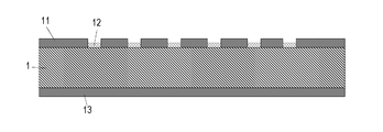
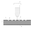
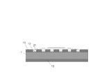
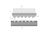
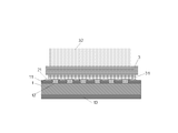
- FIG. 1 to 5 are cross-sectional views schematically showing a method for manufacturing a semiconductor device of the present invention.
- a method for manufacturing a semiconductor device of the present invention will be described.
- a substrate 1 (circuit board) is prepared.
- a wiring pattern 11 is formed on one surface side of the substrate 1 (upper side in FIG. 1), and an electrode pad portion 12 is disposed.
- a conductor layer 13 is provided on the other surface side of the substrate 1 (lower side in FIG. 1) so that a circuit pattern can be formed later.
- the thermal expansion coefficient in the thickness direction of the substrate 1 in the region of 25 ° C. or more and the glass transition temperature (Tg) or less is not particularly limited, but is preferably 20 ppm or less, and particularly preferably 5 to 18 ppm ( Hereinafter, “to” represents an upper limit value and a lower limit value unless otherwise specified). By setting it within this range, it is possible to suppress the stress caused by the difference in coefficient of linear expansion from the chip and improve the warpage.
- a paste-like thermosetting resin composition 21 having flux activity is applied so as to cover the electrode pad portion 12 of the substrate 1 (FIGS. 2 and 3).
- the means for applying is not particularly limited.
- a syringe 2 can be used.
- the application amount of the paste-like thermosetting resin composition 21 having flux activity is not particularly limited, but may be any application amount that covers at least the electrode pad portion 12 (connection portion) as shown in FIG.
- Examples of the paste-like thermosetting resin composition 21 having the flux activity include a resin composition containing a thermosetting resin and a flux activator.
- thermosetting resin for example, epoxy resin, cyanate resin, bismaleimide resin, urethane resin, polybutadiene resin, silicone resin, phenol resin, urea resin, melamine resin, unsaturated polyester resin, alkyd resin, etc. have been known so far.
- a thermosetting resin can be applied. More preferably, it is an epoxy resin.
- epoxy resin examples include bisphenol A type epoxy resin, bisphenol F type epoxy resin, bisphenol AD type epoxy resin, bisphenol E type epoxy resin, and other bisphenol type epoxy resins, phenol novolac type epoxy resins, and cresol novolak type epoxy resins.
- Novolak-type epoxy resins such as N, N-diglycidylaniline, N, N-diglycidyltoluidine, diaminodiphenylmethane-type glycidylamine, aminophenol-type glycidylamine and other aromatic glycidylamine-type epoxy resins, hydroquinone-type epoxy resins, biphenyl Biphenyl type epoxy resin such as aralkyl type epoxy resin, stilbene type epoxy resin, triphenolmethane type epoxy resin, triphenolpropane type epoxy resin Resin, alkyl-modified triphenolmethane type epoxy resin, triazine nucleus-containing epoxy resin, dicyclopentadiene-modified phenol type epoxy resin, naphthol type epoxy resin, naphthalene type epoxy resin, phenol aralkyl type epoxy resin having phenylene and / or biphenylene skeleton, Fatty substances such as epoxy resins such as aralkyl type epoxy resins such as napht
- thermosetting resin is not particularly limited, but is preferably 5 to 70% by weight, particularly preferably 10 to 50% by weight, based on the entire paste-like thermosetting resin composition 21.
- the thermal and mechanical properties such as the glass transition temperature and the elastic modulus are particularly excellent.
- the said flux activator means what has the effect
- the flux activator include phenolic compounds, acid or acid anhydride compounds, imidazoles such as amine compounds and amide compounds, and active rosins.
- phenol compound examples include tetramethylbisphenol A, catechol, resorcin, hydroquinone, xylenol, bisphenol A, bisphenol F, bisphenol AP, bisphenol S, bisphenol Z, dimethyl bisphenol A, dimethyl bisphenol F, tetramethyl bisphenol A, tetra
- Examples of the acid or acid anhydride compound include formic acid, acetic acid, propionic acid, butyric acid, valeric acid, caproic acid, enanthic acid, caprylic acid, pelargonic acid, capric acid, lauric acid, myristic acid, palmitic acid, margaric acid , Stearic acid, oleic acid, linoleic acid, linolenic acid, arachidonic acid, docosahexaenoic acid, eicosapentaenoic acid, oxalic acid, malonic acid, succinic acid, benzoic acid, phthalic acid, isophthalic acid, terephthalic acid, salicylic acid, gallic acid, melitto Acid, cinnamic acid, pyruvic acid, lactic acid, malic acid, citric acid, fumaric acid, maleic acid, aconitic acid, glutaric acid, adipic acid, pimelic acid, sube
- a compound having both a phenolic hydroxyl group and a carboxyl group may be used.
- amine compounds include ethylenediamine, 1,3-diaminopropane, 1,4-diaminobutane, diethylenetriamine, triethylenetetramine, tetraethylenepentamine, pentaethylenehexamine, dipropylenediamine, diethylaminopropylamine, tri (methyl Amino) hexane, dimethylaminopropylamine, diethylaminopropylamine, methyliminobispropylamine, hexamethylenediamine, diaminodiphenylmethane, diaminodiphenylsulfone, isophoronediamine, mensendiamine, isophoronediamine, pis (4-amino-3-methyl) Zinc cyclohexyl) methane, diaminozine cyclohexylmethane, N-aminoethylpiperazine, 3,9-bis (3-aminopropyl) 2, ,
- Examples of the amide compound include polyamide resin synthesized from dimer of dicyandiamide and linolenic acid and ethylenediamine.
- Examples of the imidazoles include 2-methylimidazole, 2-ethyl-4-methylimidazole, 2-undecylimidazole, 2-heptadecylimidazole, 2-phenyl-4,5-dihydroxymethylimidazole, 2-phenylimidazole, 2- Examples include ethyl imidazole and 2-ethyl-4-methyl imidazole. These can be used not only as flux activators but also as curing agents for those that cause a crosslinking reaction with epoxy resins.
- the content of the flux activator is not particularly limited, but is preferably 0.1 to 50% by weight, particularly preferably 1 to 40% by weight, based on the entire paste-like thermosetting resin composition 21.
- the flux activity is excellent, and particularly when used as a curing agent, in addition to excellent thermal and mechanical properties such as glass transition temperature and elastic modulus, excellent curability. .
- curing agents having flux activity compounds that have a redox action and contribute to the curing reaction with a thermosetting resin such as an epoxy resin and are incorporated in crosslinking. Thereby, flux cleaning becomes unnecessary and long-term reliability can be improved.
- the curing agent having the flux activity include phenol compounds, acid anhydrides, imidazoles, and compounds having both phenolic hydroxyl groups and carboxy groups.
- the paste-like thermosetting resin composition 21 having flux activity may contain a filler such as a curing agent, a filler, and a coupling agent in addition to the thermosetting resin and the flux activator described above.
- a filler such as a curing agent, a filler, and a coupling agent in addition to the thermosetting resin and the flux activator described above.
- the filler include silica powders such as talc, baked clay, unfired clay, mica, glass and the like, titanium oxide, alumina, fused silica (fused spherical silica, fused crushed silica), synthetic silica, and crystalline silica.
- Oxides such as calcium carbonate, magnesium carbonate, hydrotalcite, hydroxides such as aluminum hydroxide, magnesium hydroxide, calcium hydroxide, sulfates such as barium sulfate, calcium sulfate, calcium sulfite, or sulfite
- examples thereof include inorganic fillers such as salts, borates such as zinc borate, barium metaborate, aluminum borate, calcium borate, and sodium borate, and nitrides such as aluminum nitride, boron nitride, and silicon nitride.
- An organic filler may be used.
- fused silica, crystalline silica, and synthetic silica powder are preferable because reliability such as heat resistance, moisture resistance, and strength of the liquid sealing resin composition can be improved.
- the shape of the filler is not particularly limited, but the shape is preferably spherical from the viewpoint of viscosity and flow characteristics.
- the content of the filler is not particularly limited, but is preferably 20 to 90% by weight, particularly preferably 30 to 85% by weight, based on the entire paste-like thermosetting resin composition 21. If the content is less than the lower limit, the effect of improving reliability such as low linear expansion and low water absorption may be reduced. If the content exceeds the upper limit, the viscosity of the thermosetting resin composition is increased. The workability may be reduced, and the bump connectivity may be reduced.
- Examples of the coupling agent include vinyltrichlorosilane, vinyltrimethoxysilane, vinyltriethoxysilane, vinyltri- ( ⁇ -methoxyethoxy) silane, ⁇ - (3,4 epoxycyclohexyl) ethyltrimethoxysilane, and ⁇ -acryloxy.
- the content of the coupling agent is not particularly limited, but is preferably from 0.1 to 20% by weight, particularly preferably from 0.3 to 10% by weight, based on the entire paste-like thermosetting resin composition 21.
- the content is less than the lower limit, the adhesion and fluidity may be reduced, and when the content exceeds the upper limit, the volatile voidability may be reduced.
- the semiconductor element 3 is mounted on the substrate 1 using the flip chip bonder 32.
- the solder bump 31 (first conductive portion) of the semiconductor element 3 and the electrode pad portion 12 (second conductive portion) of the substrate 1 are mounted so as to be in contact with each other (FIG. 4).
- the solder bump 31 is electrically connected to the electrode pad portion 12 while being melted.
- the paste-like thermosetting resin composition 21 has a flux activity, it is possible to perform solder connection while removing the oxide film on the surface of the solder bump 31 (FIG. 5). That is, in the main joining step, the substrate 1 and the semiconductor element 3 are electrically connected so that the solder bump 31 and the electrode pad portion 12 are solder-connected in a state covered with the paste-like thermosetting resin composition 21. Join.
- connection condition is not particularly limited, but it is preferable to set the set temperature of the flip chip bonder 32 to + 10 ° C. to 100 ° C. of the melting point of the solder material used for the solder bump 31 and to heat for 1 to 30 seconds. . At this time, it is more preferable if the heating is performed only from the semiconductor element 3 side. This is because thermal stress on the substrate can be reduced, warpage caused by a difference in linear expansion coefficient from the chip can be reduced, and volatile voids derived from the substrate can also be suppressed.
- the first conductive portion and the second conductive portion are not limited to the solder bump 31 and the electrode pad portion 12, respectively, and at least one of them may be a solder bump, both of which are solder bumps. But you can.
- the means for heat-curing the paste-like thermosetting resin composition 21 is not particularly limited, and for example, an oven can be used.
- the heating condition depends on the thermosetting resin to be used and is not particularly limited, but is preferably 100 to 200 ° C. ⁇ 30 to 180 minutes, and particularly preferably 120 to 170 ° C. ⁇ 60 to 150 minutes.
- the heating temperature is equal to or higher than the glass transition temperature of the cured product of the paste-like thermosetting resin composition 21.
- the glass transition temperature of the cured product of the paste-like thermosetting resin composition 21 having flux activity after the curing step is not particularly limited, but is preferably 20 ° C to 300 ° C, and preferably 50 ° C to 150 ° C. It is particularly preferred. Bump protection can be improved more effectively by setting the glass transition temperature to the above lower limit value or more. Moreover, the crack of the fillet which consists of the paste-form thermosetting resin composition 21 which has the flux activity formed after joining the board
- the average linear expansion coefficient ( ⁇ 1) in the region of 25 ° C. or more and the glass transition temperature or less of the cured product of the paste-like thermosetting resin composition 21 having the flux activity after the curing step is not particularly limited, but is 5 ppm / ° C. It is preferably ⁇ 60 ppm / ° C., particularly preferably 15 ppm / ° C. to 40 ppm / ° C.
- the average linear expansion coefficient equal to or lower than the glass transition temperature of the cured product of the paste-like thermosetting resin composition 21 having flux activity is set to the linear expansion of the bump (solder bump 31). It can be close to the coefficient. For this reason, bump cracks can be effectively suppressed.
- the glass transition temperature and linear expansion coefficient of the cured product of the paste-like thermosetting resin composition 21 having the flux activity after the curing step can be measured by the following methods.
- the paste-like thermosetting resin composition 21 having flux activity is cured at 150 ° C. for 3 hours to prepare a sample having a size of 4 mm ⁇ 4 mm ⁇ 10 mm.
- the compression load 10 g
- the heating rate 10 ° C./min
- the measurement temperature range ⁇ 100 ° C. to 300 ° C.
- the average in the region below the glass transition temperature and the glass transition temperature Calculate the linear expansion coefficient.
- cooling is performed at a cooling rate of 10 to 50 ° C./h after the curing step.
- a means for cooling for example, a means for setting the condition of the cooling rate of the oven by continuously using the oven used in the curing step is used.
- the cooling rate may be a constant rate or a variable rate.
- the means for calculating the cooling rate can be obtained, for example, by dividing the temperature difference obtained by subtracting the temperature after the end of the cooling step from the temperature in the atmosphere immediately after the curing step by the cooling time.
- the temperature indicates, for example, the temperature in the oven atmosphere.
- thermosetting resin which is a viscoelastic body, heat distribution will generate
- the thermal contraction of the structural member due to rapid cooling occurs, and a large stress is generated due to the difference in the linear expansion coefficients of the structural members.
- the warp has occurred due to the stress caused by the rapid cooling.
- the cooling process is performed as described above. Further, after the curing step, when it is subsequently cooled at a cooling rate of 10 to 50 ° C./h, the method of thermal shrinkage becomes gentle, and further, the stress due to the difference in the coefficient of linear expansion of the constituent members can be relaxed. Therefore, in the present invention, the stress during cooling can be relaxed and the warpage can be reduced.
- the lower limit of the cooling rate (first cooling rate) is preferably 15 ° C./h or more, and more preferably 20 ° C./h or more.
- the upper limit value of the cooling rate (first cooling rate) is preferably 40 ° C./h or less, and more preferably 30 ° C./h or less.
- the temperature range for controlling the cooling rate (hereinafter sometimes referred to as the control range) is not particularly limited, but the curing temperature of the paste-like thermosetting resin composition 21 in the curing step is Tc [° C.].
- the temperature range can be Tc [° C.] to (Tc-90) [° C.]. It is preferable to cool this temperature range at the first cooling rate. Thereby, the generation of stress within the control range is more remarkable, and the effect of suppressing the occurrence of warpage is particularly excellent by controlling the temperature range.
- the control range of the first cooling rate can be a temperature range of 150 to 60 [° C.] when the curing temperature (Tc) is 150 [° C.], more preferably The temperature can be in the range of 150 to 80 [° C.]. It is preferable to cool this temperature range at the first cooling rate.
- the control range can be a temperature range of Tc [° C.] or less, (glass transition temperature of the cured product of the paste-like thermosetting resin composition 21 ⁇ 20) [° C.] or more, specifically 150 to (Glass transition temperature (Tg) -20 of the cured product of the paste-like thermosetting resin composition 21) [° C.]. It is preferable to cool this temperature range at the first cooling rate. When the control range is within such a temperature range, it is particularly excellent in suppressing warpage.
- the cooling rate outside the control range is set as the second cooling rate.
- the second cooling rate is set to 60 to 120 ° C./h. In particular, it is preferably 40 to 100 ° C./h. Thereby, it is excellent in balance with the effect which relieves stress, and favorable productivity.
- the semiconductor device can be obtained through the steps as described above, such as the formation of solder bumps for connection to the motherboard and the mounting of components.
- the semiconductor device thus obtained can protect the semiconductor elements by protecting the bumps and reducing the occurrence of warpage.
- thermosetting resin bisphenol F type epoxy resin (Dainippon Ink Chemical Co., Ltd., EXA-830LVP, epoxy equivalent 161) 70.9% by weight, as a curing agent 6.
- Phenol novolak manufactured by Sumitomo Durez Co., Ltd., product number PR-51470, softening point 110 ° C.
- phenol activator as flux activator
- thermosetting resin composition (melting point 235 ° C.)) 1% by weight and 0.7% by weight of 2-phenyl-4-methylimidazole (manufactured by Shikoku Kasei Kogyo Co., Ltd., 2P4MZ) as a curing accelerator are weighed, dispersed and kneaded with three rolls, and removed under vacuum. Foam treatment was performed to obtain a paste-like thermosetting resin composition.
- thermosetting resin composition as a core material, manufactured by Sumitomo Bakelite Co., Ltd., product number ELC-4785GS, coefficient of thermal expansion (Tg or less) XY direction: 11 ppm, Z direction: 16 ppm
- a semiconductor element having a solder bump size 15 ⁇ 15 ⁇ thickness 0.725 mm
- the paste-like thermosetting resin composition was cured by heating in an oven at 150 ° C. for 120 minutes.
- the conditions for the cooling rate of the oven are set, and the temperature range of 150 to 60 ° C. is cooled at a cooling rate of 25 ° C./h, and then the temperature is cooled to about 30 ° C. at about 60 ° C./h. Obtained.
- the temperature indicates the temperature in the oven atmosphere.
- Example 2 In the manufacturing process of a semiconductor device, it was made to be the same as that of Example 1 except having made cooling rate as follows.
- the cooling rate in the range of 150 to 60 ° C. was 15 ° C./h.
- Example 3 In the manufacturing process of the semiconductor device, it was the same as that of Example 1 except that the cooling range was as follows.
- the cooling rate in the range of 150 to 80 ° C. was set to the same cooling rate as in Example 1, and the cooling rate of less than 80 ° C. to 30 ° C. was 1 ° C./min.
- Example 4 The paste-like thermosetting resin composition was the same as Example 1 except that the following was used.
- Bisphenol F type epoxy resin (Dainippon Ink Chemical Co., Ltd., EXA-830LVP, epoxy equivalent 161) as thermosetting resin, 76.3% by weight, and 2,5-dihydroxybenzoic acid as a curing agent having flux activity 22.9% by weight (manufactured by Tokyo Chemical Industry (melting point: 200 to 205 ° C.)) and 0.8% by weight of 2-phenyl-4-methylimidazole (manufactured by Shikoku Chemicals Co., Ltd.) as a curing accelerator are weighed. Then, the mixture was dispersed and kneaded with three rolls and defoamed under vacuum to obtain a paste-like thermosetting resin composition.
- Example 5 In the manufacturing method of the semiconductor device, the same procedure as in Example 1 was performed except that the paste-like thermosetting resin composition was applied to the semiconductor element instead of the substrate.
- Example 6 The substrate was the same as Example 1 except that the following was used.
- a substrate having a core material of BT manufactured by Mitsubishi Gas Chemical Company, product number CCL-HL832HS, coefficient of thermal expansion (Tg or less) XY direction: 15 ppm, Z direction: 55 ppm was used.
- Example 1 In the manufacturing process of a semiconductor device, it was made to be the same as that of Example 1 except having made the cooling rate as follows.
- the cooling rate in the range of 150 to 60 ° C. was 5 ° C./h.
- thermosetting resin composition In the manufacturing process of a semiconductor device, the following paste-like thermosetting resin composition was injected into a semiconductor device in which a semiconductor element was previously mounted on a substrate to obtain a semiconductor package.
- the paste-like thermosetting resin composition has 79.4% by weight of a bisphenol F type epoxy resin (manufactured by Dainippon Ink and Chemicals, EXA-830 LVP, epoxy equivalent 161) as a thermosetting resin, 19.8% by weight of phenol novolac and 0.8% by weight of 2-phenyl-4-methylimidazole (manufactured by Shikoku Kasei Kogyo Co., Ltd.) as a curing accelerator were weighed and dispersed and kneaded with three rolls. Obtained by degassing under vacuum.
- a bisphenol F type epoxy resin manufactured by Dainippon Ink and Chemicals, EXA-830 LVP, epoxy equivalent 161
- 2-phenyl-4-methylimidazole manufactured by Shikoku Kasei Kogy
- the semiconductor device was held in the oven for a predetermined time while maintaining the curing temperature, and then the semiconductor device was taken out and exposed to room temperature to evaluate the warpage of the semiconductor device.
- the curing temperature was 150 ° C.
- the room temperature was 25 ° C.
- the cooling time was about 30 minutes, it is considered that the cooling was performed at a cooling rate of about 250 ° C./h or more.
- warping occurred visually.
- Warpage of Semiconductor Device The warpage of the obtained semiconductor device and the warpage of the semiconductor device after the reflow resistance test described later were evaluated. Each code was as follows. A: The amount of warpage was 80 ⁇ m or less. ⁇ : The amount of warpage exceeded 80 ⁇ m and was 100 ⁇ m or less. (Triangle
- Examples 1 to 6 had small warpage both after manufacture and after the reflow resistance test. In addition, Examples 1 to 6 were excellent in reliability. This suggested that the solder bumps were protected. In addition, Examples 1 to 6 were excellent in workability.
Landscapes
- Chemical & Material Sciences (AREA)
- Life Sciences & Earth Sciences (AREA)
- Engineering & Computer Science (AREA)
- Materials Engineering (AREA)
- Wood Science & Technology (AREA)
- Organic Chemistry (AREA)
- Wire Bonding (AREA)
- Structures Or Materials For Encapsulating Or Coating Semiconductor Devices Or Solid State Devices (AREA)
Abstract
Priority Applications (4)
| Application Number | Priority Date | Filing Date | Title |
|---|---|---|---|
| CN2009801207336A CN102057475B (zh) | 2008-06-05 | 2009-06-02 | 半导体装置的制造方法以及半导体装置 |
| JP2010515766A JP4862963B2 (ja) | 2008-06-05 | 2009-06-02 | 半導体装置の製造方法 |
| US12/993,977 US20110068483A1 (en) | 2008-06-05 | 2009-06-02 | Method of manufacturing a semiconductor device and semiconductor device |
| EP09758095A EP2284876A4 (fr) | 2008-06-05 | 2009-06-02 | Procede de production d' un dispositif a semi-conducteur et dispositif a semi-conducteur |
Applications Claiming Priority (2)
| Application Number | Priority Date | Filing Date | Title |
|---|---|---|---|
| JP2008147716 | 2008-06-05 | ||
| JP2008-147716 | 2008-06-05 |
Publications (1)
| Publication Number | Publication Date |
|---|---|
| WO2009147828A1 true WO2009147828A1 (fr) | 2009-12-10 |
Family
ID=41397911
Family Applications (1)
| Application Number | Title | Priority Date | Filing Date |
|---|---|---|---|
| PCT/JP2009/002447 Ceased WO2009147828A1 (fr) | 2008-06-05 | 2009-06-02 | Procédé de production d’un dispositif à semi-conducteur et dispositif à semi-conducteur |
Country Status (7)
| Country | Link |
|---|---|
| US (1) | US20110068483A1 (fr) |
| EP (1) | EP2284876A4 (fr) |
| JP (1) | JP4862963B2 (fr) |
| KR (1) | KR20110027714A (fr) |
| CN (1) | CN102057475B (fr) |
| TW (1) | TW201007855A (fr) |
| WO (1) | WO2009147828A1 (fr) |
Cited By (4)
| Publication number | Priority date | Publication date | Assignee | Title |
|---|---|---|---|---|
| KR101120982B1 (ko) * | 2010-05-25 | 2012-03-13 | 스테코 주식회사 | 플립 칩 접합방법 |
| JP2013187491A (ja) * | 2012-03-09 | 2013-09-19 | Hitachi Chemical Co Ltd | 回路接続構造体の製造方法 |
| WO2014092137A1 (fr) * | 2012-12-11 | 2014-06-19 | 三井金属鉱業株式会社 | Carte de circuits imprimés multicouche et son procédé de fabrication |
| JPWO2022158527A1 (fr) * | 2021-01-20 | 2022-07-28 |
Families Citing this family (7)
| Publication number | Priority date | Publication date | Assignee | Title |
|---|---|---|---|---|
| US9099444B2 (en) * | 2011-12-22 | 2015-08-04 | Intel Corporation | 3D integrated circuit package with through-mold first level interconnects |
| JP2014091744A (ja) * | 2012-10-31 | 2014-05-19 | 3M Innovative Properties Co | アンダーフィル組成物、半導体装置およびその製造方法 |
| IL223414A (en) * | 2012-12-04 | 2017-07-31 | Elta Systems Ltd | Integrated electronic device and method for creating it |
| JP2016162985A (ja) * | 2015-03-05 | 2016-09-05 | ルネサスエレクトロニクス株式会社 | 半導体装置の製造方法 |
| JP6540833B1 (ja) * | 2018-01-17 | 2019-07-10 | 千住金属工業株式会社 | フラックス及びソルダペースト |
| CN112338346B (zh) * | 2020-10-29 | 2022-11-04 | 河海大学常州校区 | 一种采用瞬间液相扩散焊连接蓝宝石的方法 |
| EP4368651A1 (fr) * | 2022-11-09 | 2024-05-15 | Sika Technology AG | Durcisseurs pour résines époxydes contenant de l'acide diphénolique |
Citations (4)
| Publication number | Priority date | Publication date | Assignee | Title |
|---|---|---|---|---|
| JPH07335791A (ja) | 1994-06-13 | 1995-12-22 | Shin Etsu Chem Co Ltd | 半導体装置 |
| JPH10204259A (ja) | 1997-01-17 | 1998-08-04 | Loctite Corp | 熱硬化性樹脂組成物 |
| JP2004067930A (ja) * | 2002-08-08 | 2004-03-04 | Sumitomo Bakelite Co Ltd | 液状封止樹脂組成物及びこれを用いた半導体装置並びに半導体装置の製造方法 |
| JP2007005557A (ja) * | 2005-06-23 | 2007-01-11 | Sumitomo Electric Ind Ltd | 電子部品の実装方法 |
Family Cites Families (13)
| Publication number | Priority date | Publication date | Assignee | Title |
|---|---|---|---|---|
| JPH08300494A (ja) * | 1995-05-09 | 1996-11-19 | Toshinori Okuno | 熱硬化性樹脂成形品の後処理方法 |
| JP3533665B1 (ja) * | 2002-12-17 | 2004-05-31 | オムロン株式会社 | 電子部品モジュールの製造方法、並びに電磁波読み取り可能なデータキャリアの製造方法。 |
| JP3971995B2 (ja) * | 2002-12-25 | 2007-09-05 | 日本電気株式会社 | 電子部品装置 |
| JP2004204047A (ja) * | 2002-12-25 | 2004-07-22 | Nitto Denko Corp | 液状エポキシ樹脂組成物 |
| JP2004235522A (ja) * | 2003-01-31 | 2004-08-19 | Optrex Corp | 半導体装置およびその製造方法 |
| JP4001341B2 (ja) * | 2003-11-07 | 2007-10-31 | 日本Cmo株式会社 | ボンディング方法およびその装置 |
| US20070164079A1 (en) * | 2004-02-24 | 2007-07-19 | Matsushita Electric Industrial Co., Ltd. | Electronic component mounting method, and circuit substrate and circuit substrate unit used in the method |
| WO2005093817A1 (fr) * | 2004-03-29 | 2005-10-06 | Nec Corporation | Dispositif semi-conducteur et procede de fabrication dudit dispositif |
| EP1589797A3 (fr) * | 2004-04-19 | 2008-07-30 | Matsushita Electric Industrial Co., Ltd. | Procédé de fabrication de substrat laminé, et appareil de fabrication de dispositif semi-conducteur pour module et substrat laminé l'utilisant |
| JP4356581B2 (ja) * | 2004-10-12 | 2009-11-04 | パナソニック株式会社 | 電子部品実装方法 |
| JP4929964B2 (ja) * | 2006-10-12 | 2012-05-09 | 住友化学株式会社 | 樹脂多層板の製造方法 |
| EP2099036A4 (fr) * | 2006-12-26 | 2011-07-06 | Sumitomo Bakelite Co | Pâte conductrice |
| JP4518101B2 (ja) * | 2007-05-14 | 2010-08-04 | 日立化成工業株式会社 | 実装方法 |
-
2009
- 2009-06-02 WO PCT/JP2009/002447 patent/WO2009147828A1/fr not_active Ceased
- 2009-06-02 US US12/993,977 patent/US20110068483A1/en not_active Abandoned
- 2009-06-02 KR KR1020107029348A patent/KR20110027714A/ko not_active Abandoned
- 2009-06-02 EP EP09758095A patent/EP2284876A4/fr not_active Withdrawn
- 2009-06-02 JP JP2010515766A patent/JP4862963B2/ja not_active Expired - Fee Related
- 2009-06-02 CN CN2009801207336A patent/CN102057475B/zh not_active Expired - Fee Related
- 2009-06-05 TW TW098118688A patent/TW201007855A/zh unknown
Patent Citations (4)
| Publication number | Priority date | Publication date | Assignee | Title |
|---|---|---|---|---|
| JPH07335791A (ja) | 1994-06-13 | 1995-12-22 | Shin Etsu Chem Co Ltd | 半導体装置 |
| JPH10204259A (ja) | 1997-01-17 | 1998-08-04 | Loctite Corp | 熱硬化性樹脂組成物 |
| JP2004067930A (ja) * | 2002-08-08 | 2004-03-04 | Sumitomo Bakelite Co Ltd | 液状封止樹脂組成物及びこれを用いた半導体装置並びに半導体装置の製造方法 |
| JP2007005557A (ja) * | 2005-06-23 | 2007-01-11 | Sumitomo Electric Ind Ltd | 電子部品の実装方法 |
Non-Patent Citations (1)
| Title |
|---|
| See also references of EP2284876A4 |
Cited By (10)
| Publication number | Priority date | Publication date | Assignee | Title |
|---|---|---|---|---|
| KR101120982B1 (ko) * | 2010-05-25 | 2012-03-13 | 스테코 주식회사 | 플립 칩 접합방법 |
| JP2013187491A (ja) * | 2012-03-09 | 2013-09-19 | Hitachi Chemical Co Ltd | 回路接続構造体の製造方法 |
| WO2014092137A1 (fr) * | 2012-12-11 | 2014-06-19 | 三井金属鉱業株式会社 | Carte de circuits imprimés multicouche et son procédé de fabrication |
| CN104823530A (zh) * | 2012-12-11 | 2015-08-05 | 三井金属矿业株式会社 | 多层印刷布线板及其制造方法 |
| JPWO2014092137A1 (ja) * | 2012-12-11 | 2017-01-12 | 三井金属鉱業株式会社 | 多層プリント配線板及びその製造方法 |
| JPWO2022158527A1 (fr) * | 2021-01-20 | 2022-07-28 | ||
| WO2022158527A1 (fr) * | 2021-01-20 | 2022-07-28 | 積水化学工業株式会社 | Flux non électroconducteur, structure connectée et procédé de production d'une structure connectée |
| JP7592719B2 (ja) | 2021-01-20 | 2024-12-02 | 積水化学工業株式会社 | 非導電性フラックス、接続構造体及び接続構造体の製造方法 |
| JP2025032138A (ja) * | 2021-01-20 | 2025-03-11 | 積水化学工業株式会社 | 非導電性フラックス、接続構造体及び接続構造体の製造方法 |
| US12589452B2 (en) | 2021-01-20 | 2026-03-31 | Sekisui Chemical Co., Ltd. | Non-electroconductive flux, connected structure, and method for producing connected structure |
Also Published As
| Publication number | Publication date |
|---|---|
| TW201007855A (en) | 2010-02-16 |
| CN102057475B (zh) | 2013-01-02 |
| EP2284876A1 (fr) | 2011-02-16 |
| JPWO2009147828A1 (ja) | 2011-10-20 |
| EP2284876A4 (fr) | 2012-01-04 |
| JP4862963B2 (ja) | 2012-01-25 |
| US20110068483A1 (en) | 2011-03-24 |
| CN102057475A (zh) | 2011-05-11 |
| KR20110027714A (ko) | 2011-03-16 |
Similar Documents
| Publication | Publication Date | Title |
|---|---|---|
| JP4862963B2 (ja) | 半導体装置の製造方法 | |
| JP4802246B2 (ja) | 半導体装置 | |
| JP5660272B2 (ja) | フリップチップ半導体パッケージ用の接続構造、ビルドアップ層材料、封止樹脂組成物および回路基板 | |
| WO2011033743A1 (fr) | Film adhésif, carte de circuit imprimé multicouche, composant électronique et dispositif à semi-conducteur | |
| JP5353449B2 (ja) | 半導体装置の製造方法、半導体封止用接着剤及び半導体装置 | |
| WO2010029726A1 (fr) | Dispositif à semi-conducteur et composition de résine utilisée dans un dispositif à semi-conducteur | |
| WO2004059721A1 (fr) | Unite de composant electronique | |
| EP3051580B1 (fr) | Matériau de remplissage et procédé de production de dispositif à semi-conducteurs à l'aide dudit matériau de remplissage | |
| TW201945423A (zh) | 底部填充材、及使用其之半導體裝置之製造方法 | |
| WO2012157665A1 (fr) | Composant de module semi-conducteur et composition de résine liquide pour une encapsulation | |
| JP2016192501A (ja) | 半導体装置の製造方法 | |
| JP5904302B1 (ja) | 半導体装置の製造方法及び樹脂組成物 | |
| JP3376312B2 (ja) | 半導体装置用接着剤組成物、接着シート及びそれを使用した補強部材 | |
| JP5950006B2 (ja) | 半導体装置の製造方法および電子部品の製造方法 | |
| JP6189148B2 (ja) | エポキシ樹脂組成物および半導体装置 | |
| JP5909318B2 (ja) | 電子部品実装体、および電子部品の実装方法 | |
| WO2025126777A1 (fr) | Composition de résine époxyde, produit durci et dispositif à semi-conducteur | |
| JP5958799B2 (ja) | 半導体封止用液状エポキシ樹脂組成物とそれを用いた半導体装置 | |
| JP2013071941A (ja) | 半導体封止充てん用エポキシ樹脂組成物、半導体装置の製造方法、半導体装置 | |
| JP2011195743A (ja) | 液状封止樹脂組成物および半導体パッケージ | |
| JP2009283621A (ja) | 半導体装置および半導体装置の製造方法 | |
| JP2013221122A (ja) | 三次元積層型半導体装置用の層間充填剤組成物およびその塗布液 | |
| JP2011077199A (ja) | 半導体パッケージおよび半導体装置 | |
| JP2005327654A (ja) | 接続材料 |
Legal Events
| Date | Code | Title | Description |
|---|---|---|---|
| WWE | Wipo information: entry into national phase |
Ref document number: 200980120733.6 Country of ref document: CN |
|
| 121 | Ep: the epo has been informed by wipo that ep was designated in this application |
Ref document number: 09758095 Country of ref document: EP Kind code of ref document: A1 |
|
| WWE | Wipo information: entry into national phase |
Ref document number: 2010515766 Country of ref document: JP |
|
| WWE | Wipo information: entry into national phase |
Ref document number: 12010502535 Country of ref document: PH |
|
| WWE | Wipo information: entry into national phase |
Ref document number: 2009758095 Country of ref document: EP |
|
| WWE | Wipo information: entry into national phase |
Ref document number: 12993977 Country of ref document: US |
|
| NENP | Non-entry into the national phase |
Ref country code: DE |
|
| ENP | Entry into the national phase |
Ref document number: 20107029348 Country of ref document: KR Kind code of ref document: A |