WO2010018655A1 - 中継端子部材及びそれを備えた回路構造体、並びに電子ユニット - Google Patents
中継端子部材及びそれを備えた回路構造体、並びに電子ユニット Download PDFInfo
- Publication number
- WO2010018655A1 WO2010018655A1 PCT/JP2009/003408 JP2009003408W WO2010018655A1 WO 2010018655 A1 WO2010018655 A1 WO 2010018655A1 JP 2009003408 W JP2009003408 W JP 2009003408W WO 2010018655 A1 WO2010018655 A1 WO 2010018655A1
- Authority
- WO
- WIPO (PCT)
- Prior art keywords
- relay terminal
- terminal
- opening
- circuit board
- connector
- Prior art date
- Legal status (The legal status is an assumption and is not a legal conclusion. Google has not performed a legal analysis and makes no representation as to the accuracy of the status listed.)
- Ceased
Links
Images








Classifications
-
- H—ELECTRICITY
- H05—ELECTRIC TECHNIQUES NOT OTHERWISE PROVIDED FOR
- H05K—PRINTED CIRCUITS; CASINGS OR CONSTRUCTIONAL DETAILS OF ELECTRIC APPARATUS; MANUFACTURE OF ASSEMBLAGES OF ELECTRICAL COMPONENTS
- H05K7/00—Constructional details common to different types of electric apparatus
- H05K7/20—Modifications to facilitate cooling, ventilating, or heating
- H05K7/20845—Modifications to facilitate cooling, ventilating, or heating for automotive electronic casings
- H05K7/20854—Heat transfer by conduction from internal heat source to heat radiating structure
-
- H—ELECTRICITY
- H01—ELECTRIC ELEMENTS
- H01R—ELECTRICALLY-CONDUCTIVE CONNECTIONS; STRUCTURAL ASSOCIATIONS OF A PLURALITY OF MUTUALLY-INSULATED ELECTRICAL CONNECTING ELEMENTS; COUPLING DEVICES; CURRENT COLLECTORS
- H01R31/00—Coupling parts supported only by co-operation with counterpart
- H01R31/06—Intermediate parts for linking two coupling parts, e.g. adapter
-
- H—ELECTRICITY
- H01—ELECTRIC ELEMENTS
- H01R—ELECTRICALLY-CONDUCTIVE CONNECTIONS; STRUCTURAL ASSOCIATIONS OF A PLURALITY OF MUTUALLY-INSULATED ELECTRICAL CONNECTING ELEMENTS; COUPLING DEVICES; CURRENT COLLECTORS
- H01R12/00—Structural associations of a plurality of mutually-insulated electrical connecting elements, specially adapted for printed circuits, e.g. printed circuit boards [PCB], flat or ribbon cables, or like generally planar structures, e.g. terminal strips, terminal blocks; Coupling devices specially adapted for printed circuits, flat or ribbon cables, or like generally planar structures; Terminals specially adapted for contact with, or insertion into, printed circuits, flat or ribbon cables, or like generally planar structures
- H01R12/50—Fixed connections
- H01R12/51—Fixed connections for rigid printed circuits or like structures
- H01R12/55—Fixed connections for rigid printed circuits or like structures characterised by the terminals
- H01R12/57—Fixed connections for rigid printed circuits or like structures characterised by the terminals surface mounting terminals
-
- H—ELECTRICITY
- H01—ELECTRIC ELEMENTS
- H01R—ELECTRICALLY-CONDUCTIVE CONNECTIONS; STRUCTURAL ASSOCIATIONS OF A PLURALITY OF MUTUALLY-INSULATED ELECTRICAL CONNECTING ELEMENTS; COUPLING DEVICES; CURRENT COLLECTORS
- H01R12/00—Structural associations of a plurality of mutually-insulated electrical connecting elements, specially adapted for printed circuits, e.g. printed circuit boards [PCB], flat or ribbon cables, or like generally planar structures, e.g. terminal strips, terminal blocks; Coupling devices specially adapted for printed circuits, flat or ribbon cables, or like generally planar structures; Terminals specially adapted for contact with, or insertion into, printed circuits, flat or ribbon cables, or like generally planar structures
- H01R12/70—Coupling devices
- H01R12/71—Coupling devices for rigid printing circuits or like structures
-
- H—ELECTRICITY
- H01—ELECTRIC ELEMENTS
- H01R—ELECTRICALLY-CONDUCTIVE CONNECTIONS; STRUCTURAL ASSOCIATIONS OF A PLURALITY OF MUTUALLY-INSULATED ELECTRICAL CONNECTING ELEMENTS; COUPLING DEVICES; CURRENT COLLECTORS
- H01R33/00—Coupling devices specially adapted for supporting apparatus and having one part acting as a holder providing support and electrical connection via a counterpart which is structurally associated with the apparatus, e.g. lamp holders; Separate parts thereof
- H01R33/74—Devices having four or more poles, e.g. holders for compact fluorescent lamps
- H01R33/76—Holders with sockets, clips, or analogous contacts adapted for axially-sliding engagement with parallely-arranged pins, blades, or analogous contacts on counterpart, e.g. electronic tube socket
-
- H—ELECTRICITY
- H01—ELECTRIC ELEMENTS
- H01R—ELECTRICALLY-CONDUCTIVE CONNECTIONS; STRUCTURAL ASSOCIATIONS OF A PLURALITY OF MUTUALLY-INSULATED ELECTRICAL CONNECTING ELEMENTS; COUPLING DEVICES; CURRENT COLLECTORS
- H01R12/00—Structural associations of a plurality of mutually-insulated electrical connecting elements, specially adapted for printed circuits, e.g. printed circuit boards [PCB], flat or ribbon cables, or like generally planar structures, e.g. terminal strips, terminal blocks; Coupling devices specially adapted for printed circuits, flat or ribbon cables, or like generally planar structures; Terminals specially adapted for contact with, or insertion into, printed circuits, flat or ribbon cables, or like generally planar structures
- H01R12/50—Fixed connections
- H01R12/51—Fixed connections for rigid printed circuits or like structures
- H01R12/55—Fixed connections for rigid printed circuits or like structures characterised by the terminals
- H01R12/58—Fixed connections for rigid printed circuits or like structures characterised by the terminals terminals for insertion into holes
-
- H—ELECTRICITY
- H01—ELECTRIC ELEMENTS
- H01R—ELECTRICALLY-CONDUCTIVE CONNECTIONS; STRUCTURAL ASSOCIATIONS OF A PLURALITY OF MUTUALLY-INSULATED ELECTRICAL CONNECTING ELEMENTS; COUPLING DEVICES; CURRENT COLLECTORS
- H01R12/00—Structural associations of a plurality of mutually-insulated electrical connecting elements, specially adapted for printed circuits, e.g. printed circuit boards [PCB], flat or ribbon cables, or like generally planar structures, e.g. terminal strips, terminal blocks; Coupling devices specially adapted for printed circuits, flat or ribbon cables, or like generally planar structures; Terminals specially adapted for contact with, or insertion into, printed circuits, flat or ribbon cables, or like generally planar structures
- H01R12/70—Coupling devices
- H01R12/71—Coupling devices for rigid printing circuits or like structures
- H01R12/72—Coupling devices for rigid printing circuits or like structures coupling with the edge of the rigid printed circuits or like structures
- H01R12/722—Coupling devices for rigid printing circuits or like structures coupling with the edge of the rigid printed circuits or like structures coupling devices mounted on the edge of the printed circuits
- H01R12/724—Coupling devices for rigid printing circuits or like structures coupling with the edge of the rigid printed circuits or like structures coupling devices mounted on the edge of the printed circuits containing contact members forming a right angle
-
- H—ELECTRICITY
- H01—ELECTRIC ELEMENTS
- H01R—ELECTRICALLY-CONDUCTIVE CONNECTIONS; STRUCTURAL ASSOCIATIONS OF A PLURALITY OF MUTUALLY-INSULATED ELECTRICAL CONNECTING ELEMENTS; COUPLING DEVICES; CURRENT COLLECTORS
- H01R2107/00—Four or more poles
-
- H—ELECTRICITY
- H01—ELECTRIC ELEMENTS
- H01R—ELECTRICALLY-CONDUCTIVE CONNECTIONS; STRUCTURAL ASSOCIATIONS OF A PLURALITY OF MUTUALLY-INSULATED ELECTRICAL CONNECTING ELEMENTS; COUPLING DEVICES; CURRENT COLLECTORS
- H01R2201/00—Connectors or connections adapted for particular applications
- H01R2201/26—Connectors or connections adapted for particular applications for vehicles
Definitions
- the present invention relates to a relay terminal member, a circuit structure including the relay terminal member, and an electronic unit.
- the surface mount connector of Patent Document 1 includes an insulating housing and a plurality of conductive terminals having a held portion held by the housing and one end portion being a mounting end portion mounted on a substrate. It has.
- the housing is provided with a gap that is located between the upper surface of the housing and the held portion and suppresses heat conduction from the housing upper surface to the held portion side.
- the surface mount connector of Patent Document 2 includes an insulating housing that is fixed to a circuit board while holding a plurality of terminals connected to the circuit board.
- the insulating housing includes a back wall portion that is erected with respect to the circuit board and can hold a plurality of terminals arranged in at least a direction along the circuit board, and the back wall portion includes the back wall portion.
- a lateral slit portion extending in a direction along the circuit board.
- the horizontal slit part is provided in the position below the uppermost terminal press-fitting hole among the plurality of terminal press-fitting holes formed in the back wall part.
- cream solder is generally used when components are surface-mounted on a circuit board. That is, first, cream solder is applied to the soldered portion of the printed wiring on the circuit board. Thereafter, the component is placed on the cream solder, and then placed in a high-temperature furnace to melt the cream solder in a short time and solder the component to the circuit board.
- the amount of cream solder can be finely adjusted, and even a high-density IC (VLSI) or a solder bridge can be used for high-density soldering.
- VLSI high-density IC
- solder bridge can be used for high-density soldering.
- the connector housing is generally made of inexpensive general-purpose resin having thermoplasticity, it may be deformed by high temperature when placed in the furnace for soldering. As a result, there is a problem that the reliability of the connector is lowered.
- the present invention has been made in view of such a point, and an object of the present invention is to improve reliability by preventing deformation due to high temperature of a surface-mounted connector while using an inexpensive general-purpose connector. There is to try.
- a relay terminal member includes a plate-like main body portion having an opening formed therethrough, and a terminal portion formed integrally with the main body portion and connected to a circuit board.
- the covering portion has a plurality of holes formed at positions corresponding to the opening portions of the relay terminals, and the terminal pins of the connector are inserted into the opening portions of the relay terminals.
- the opening portion of the main body portion of the relay terminal has a cut portion that is cut radially outward of the opening portion.
- a circuit structure includes a circuit board, a connector, and a relay terminal member configured to relay the circuit board and the connector so that they are electrically connected to each other.
- a plurality of relay terminals having a plate-like main body portion through which is formed and a terminal portion integrally formed with the main body portion and connected to the circuit board, while exposing the terminal portion of the relay terminal,
- a cover portion made of an insulating material covering the main body portion of the relay terminal, and the cover portion has a plurality of holes that are formed so as to penetrate the relay terminal at positions corresponding to the openings of the relay terminal.
- the opening portion of the main body portion of the relay terminal has a cut portion that is cut radially outward of the opening portion.
- an electronic unit according to the present invention includes the above circuit structure.
- the terminal pin of the connector is inserted into the opening of the relay terminal. If it does so, a part of main-body part around an opening part will deform
- the terminal pin of the connector is inserted into the opening portion of the relay terminal, and the main body portion of the relay terminal is deformed around the opening portion. Therefore, the terminal pin and the relay terminal can be used without using solder. Can be conducted.
- the connector after connecting the relay terminal member to the circuit board with solder in a high temperature environment, the connector can be connected to the relay terminal member in a room temperature environment, so it is possible to use a general-purpose connector with low heat resistance become. That is, while using an inexpensive general-purpose connector as a surface-mounted connector on a circuit board, it is possible to improve the reliability by preventing deformation of the connector due to high temperature.
- the opening has a cut portion cut out to the outside, a part of the main body around the opening can be easily deformed when the terminal pin is inserted.
- the tip portion of the terminal pin inserted into the opening is not penetrated to the back side of the circuit board. It can be arranged in the gap. Therefore, the back side of the circuit board can be used effectively.
- the relay terminal member includes a relay terminal having a terminal portion connected to the circuit board and a main body portion formed with an opening portion into which the terminal pin of the connector is inserted and connected. Therefore, after soldering the terminal portion of the relay terminal member to the circuit board in a high temperature environment, the connector can be connected to the opening portion of the relay terminal member in a room temperature environment.
- a connector can be used. That is, while using an inexpensive general-purpose connector as a connector to be surface-mounted on a circuit board, the connector can be prevented from being deformed due to high temperature and reliability can be improved.
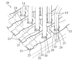
- FIG. 1 is a perspective view showing the appearance of the circuit structure according to the first embodiment.
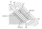
- FIG. 2 is a perspective view showing the opening of the relay terminal member to which the terminal pin is inserted and connected.
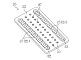
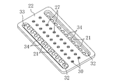
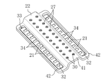
- FIG. 3 is a perspective view illustrating an appearance of the relay terminal member according to the first embodiment. 4 is an enlarged perspective view showing a part of FIG.
- FIG. 5 is a plan view of the opening and the hole when the tip of the terminal pin is inserted.
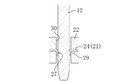
- FIG. 6 is a longitudinal sectional view of the opening and the hole when the tip of the terminal pin is inserted.
- FIG. 7 is a plan view of the opening and the hole when the tip of the terminal pin is inserted and penetrated.
- FIG. 1 is a perspective view showing the appearance of the circuit structure according to the first embodiment.
- FIG. 2 is a perspective view showing the opening of the relay terminal member to which the terminal pin is inserted and connected.
- FIG. 8 is a longitudinal sectional view of the opening and the hole when the tip of the terminal pin is inserted and penetrated.
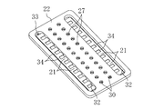
- FIG. 9 is a perspective view showing the appearance of the relay terminal before cutting in the first embodiment.
- FIG. 10 is a perspective view showing an appearance of the relay terminal before being cut into a step shape.
- FIG. 11 is an enlarged perspective view showing a part of FIG.
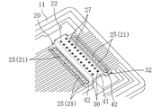
- FIG. 12 is a perspective view showing the relay terminal member connected to the circuit board according to the first embodiment.
- FIG. 13 is a perspective view showing an appearance of the circuit structure according to the second embodiment.
- FIG. 14 is a perspective view showing the opening of the relay terminal member to which the terminal pin is inserted and connected.
- FIG. 15 is a perspective view illustrating an appearance of the relay terminal member according to the second embodiment.
- FIG. 16 is an enlarged perspective view showing a part of FIG.
- FIG. 17 is a perspective view showing an appearance of the relay terminal before cutting in the second embodiment.
- FIG. 18 is a perspective view showing
- Embodiment 1 of the Invention 1 to 12 show Embodiment 1 of the present invention.
- FIG. 1 is a perspective view showing an appearance of the circuit structure 10 according to the first embodiment.
- FIG. 2 is a perspective view showing the opening 27 of the relay terminal member 20 to which the terminal pin 14 is inserted and connected.
- FIG. 5 is a plan view of the opening 27 and the hole 30 when the tip of the terminal pin 14 is inserted.
- FIG. 6 is a longitudinal sectional view of the opening 27 and the hole 30 when the tip of the terminal pin 14 is inserted.
- FIG. 7 is a plan view of the opening 27 and the hole 30 when the tip of the terminal pin 14 is inserted and penetrated.
- FIG. 8 is a longitudinal sectional view of the opening 27 and the hole 30 when the tip of the terminal pin 14 is inserted and penetrated.
- the circuit structure 10 includes a circuit board 11, a connector 12, and a relay terminal member 20 configured to relay the circuit board 11 and the connector 12 and to conduct each other. It has.
- the circuit board 11 is a so-called printed board, and a wiring pattern made of copper foil is formed on the surface of the insulating substrate, and the wiring pattern is covered with a solder resist.
- a plurality of terminals (not shown) for connecting the relay terminal members are formed, for example, arranged in 2 ⁇ 12 rows. The plurality of terminals are exposed without being covered with the solder resist.
- the connector 12 includes an insulating housing 13 and a plurality of terminal pins 14 that extend through one side surface of the insulating housing 13 to the outside.
- the insulating housing 13 can be formed of a general-purpose resin. Examples of the general-purpose resin include polybutylene terephthalate (PBT) and resins such as nylon. Moreover, in order to improve the mold retention, glass fibers or the like may be added to these resins.
- a locking claw (not shown) for locking and fixing the connector 12 to the circuit board 11 is formed on the bottom surface of the insulating housing 13.
- the circuit board 11 is formed with an engagement hole (not shown) that engages with a locking claw of the connector 12.
- the terminal pins 14 are similarly arranged in 2 ⁇ 12 rows corresponding to the plurality of terminals of the circuit board 11.
- the plurality of terminal pins 14 are formed of, for example, a metal material such as copper, and are formed in a substantially L shape that extends laterally from the side surface of the insulating housing 13 and is bent downward.
- the cross section of the terminal pin 14 is formed in, for example, a rectangular cross section of 0.5 mm square.
- the tip of the terminal pin 14 is pressed into a pointed quadrangular pyramid surface.
- the cross-sectional shape of the terminal pin 14 is not limited to this, and may be formed in other polygonal shapes, for example.
- the relay terminal member 20 includes a plurality of plate-like relay terminals 21 made of a metal material such as copper, and a covering portion 22 that covers a part of the relay terminal 21. ing.
- the relay terminal 21 has a plate-like main body 24 and a terminal 25 formed integrally with the main body 24 as shown in an enlarged view in FIG.
- the terminal portion 25 is formed integrally with the main body portion 24, and as shown in FIG. 2, the tip end is formed in a stepped shape with one step down on the surface side of the circuit board 11. As a result, the tip of the terminal portion 25 is connected to the terminal of the circuit board 11.
- the covering portion 22 is formed in a plate shape and is made of an insulating material, and is formed of, for example, polyphenylene sulfide resin (PPS) which is a heat resistant resin. As shown in FIG. 1, the covering portion 22 has two slit-like opening grooves 32 extending in parallel, and the terminal portions 25 of the relay terminals 21 are exposed in a line in the opening grooves 32. ing.
- PPS polyphenylene sulfide resin
- the main body 24 is formed in a plate shape and has an opening 27 formed therethrough.
- the opening 27 is for inserting the terminal pin 14 of the connector 12.
- the opening 27 is formed at a symmetrical position with respect to the center, and is cut out 4 in the radial direction.
- a convex portion 29 that is curved and protrudes inside the opening 27 is formed between the adjacent cut portions 28.
- the opening 27 is inserted into the terminal pin 14 so that the four corners of the terminal pin 14 are in contact with the convex portion 29. Yes.
- the main body 24 is embedded and covered at a central position in the thickness direction of the plate-like covering portion 22.
- the covering portion 22 has a plurality of hole portions 30 formed so as to penetrate at positions corresponding to the opening portions 27 of the relay terminals 21.
- the hole 30 is formed in, for example, a circular shape, and the tip of the convex portion 29 protrudes therein.
- the opening 27 of the relay terminal 21 has a convex portion 29 that is a part of the main body 24 around the opening 27 when the terminal pin 14 of the connector 12 is inserted.
- the tip end portion of the cover portion 22 is deformed to the inner wall side of the hole portion 30 of the covering portion 22, and the tip end portion of the convex portion 29 is configured to contact the terminal pin 14 of the connector 12.
- the electronic unit includes the circuit structure 10 and a housing (not shown) that stores the circuit structure 10.
- the casing is formed, for example, in a substantially rectangular parallelepiped shape as a whole, and is configured by a flat plate-like lid (not shown) and a casing body (not shown) whose opening is closed by the lid. Yes.
- a circuit board 11 of the circuit structure 10 is mounted on the back side of the lid (that is, inside the housing).
- a socket portion (not shown) is formed on the housing 13 of the connector 12 on the side opposite to the side where the terminal pins 14 are provided.
- an opening (not shown) into which the socket portion is inserted is formed on the side surface of the housing body. Then, with the socket portion of the connector 12 fitted into the opening of the housing body, the lid portion is attached to the open portion of the housing body and closed.
- the lid can be fixed to the housing body by, for example, screw fixing or engagement fixing. Thus, the electronic unit is manufactured.
- circuit structure 10 may be attached to the housing body other than the lid portion of the housing, or may be attached to both the lid portion and the housing body.
- FIG. 9 is a perspective view showing an appearance of the relay terminal 21 before cutting in the first embodiment.
- FIG. 10 is a perspective view showing an appearance of the relay terminal 21 before being cut into a step shape.
- FIG. 11 is an enlarged perspective view showing a part of FIG.
- an assembly 33 of relay terminals 21 made of a thin metal plate such as copper is formed by pressing.
- the terminal portions 25 are integrally connected by a connecting portion 34.
- An opening 27 is formed in the assembly 33 at the same time.
- the assembly 33 is loaded into a mold (not shown)
- molten PPS resin is injected into the mold so as to wrap the assembly 33.
- the covering portion 22 is formed by injection molding.
- the opening groove 32 and the hole 30 are formed in the covering portion 22.
- both side portions of the assembly 33 covered with the covering portion 22 are pressed in the opening groove 32 to form a stepped shape.
- the plurality of relay terminals 21 are formed by cutting and removing the connecting portions 34 in the assembly 33 processed into a stepped shape.
- the relay terminal member 20 is manufactured by the above process.
- FIG. 12 is a perspective view showing the relay terminal member 20 connected to the circuit board 11 in the first embodiment.
- cream solder is applied to a plurality of terminals on the circuit board 11, and the terminal portions 25 of the relay terminal member 20 are placed on the cream solder as shown in FIG. Subsequently, by moving the relay terminal member 20 and the circuit board 11 to the inside of the high-temperature furnace, the cream solder is melted and cured in a short time, whereby the plurality of terminal portions 25 of the relay terminal member 20 are connected to the circuit. Each of the plurality of terminals on the substrate 11 is soldered. At this time, since the covering portion 22 of the relay terminal member 20 is formed of heat-resistant PPS resin, it is not deformed by the heating.
- the connector 12 is connected to the relay terminal member 20 as shown in FIG.
- the plurality of terminal pins 14 of the connector 12 are respectively inserted into the openings 27 in the holes 30 in the relay terminal member 20, and the insulating housing 13 of the connector 12 is engaged and fixed to the circuit board 11.
- the “deformation” includes elastic deformation and plastic deformation.
- the tip portion of the convex portion 29 is deformed and bent toward the inner wall side of the hole portion 30. This bending may be bending by elastic deformation or bending by plastic deformation.
- the tip portion of the bent convex portion 29 has a gap between the inner wall of the hole portion 30 and the terminal pin 14 inserted into the hole portion 30. Is fitted between the inner wall of the hole 30 and the terminal pin 14.
- the terminal pin 14 of the connector 12 is electrically connected to the relay terminal 21 at the convex portion 29 of the main body 24 of the relay terminal 21 of the relay terminal member 20, while the relay terminal 21 is connected to the circuit board 11 at the terminal portion 25. Since the terminal 12 is electrically connected, the connector 12 is electrically connected to the circuit board 11 via the relay terminal member 20. In addition, the tip of the terminal pin 14 is in a state of protruding to the back surface side through a through hole (not shown) formed in the circuit board 11.
- the circuit structure 10 is manufactured through the above steps.
- the relay terminal member 20 includes the main body portion 24 in which the terminal portion 25 connected to the circuit board 11 and the opening portion 27 into which the terminal pin 14 of the connector 12 is inserted and connected are formed. Since the terminal portion 25 of the relay terminal member 20 is solder-connected to the circuit board 11 inside the furnace in a high temperature environment, the relay terminal member 20 is connected in the room temperature environment. Since the terminal pin 14 of the connector 12 can be connected to the opening 27, a general-purpose connector 12 having low heat resistance can be used. That is, while using an inexpensive general-purpose connector as the connector 12 to be surface-mounted on the circuit board 11, the connector 12 can be prevented from being deformed due to high temperature and reliability can be improved.
- the opening 27 has a cut portion 28 cut out to the outside, it is a part of the main body 24 around the opening 27 when the terminal pin 14 is inserted into the opening 27.
- the tip portion of the convex portion 29 can be easily bent and deformed.
- the conduction structure is formed by inserting the terminal pin 14 into the opening 27, a receiving terminal is provided which hinders the high density of electronic components mounted on the circuit board 11 and the narrow pitch of the hole 30. It is not necessary. Therefore, a connector having terminals with a narrow pitch and a multistage arrangement can be applied to the circuit structure 10. Moreover, it is not necessary to provide a receiving terminal forming step separately.
- the terminal pin 14 is inserted into the opening 27 of the relay terminal 21 and the tip end portion of the convex portion 29 of the relay terminal 21 is bent and deformed, there is a slight error in the size and position of the opening 27. Even if it exists, the terminal pin 14 can be inserted and conducted without any problem. For this reason, the manufacturing efficiency of the circuit structure 10 can be improved, and the manufacturing cost can be reduced.
- Embodiment 2 of the Invention >> 13 to 18 show Embodiment 2 of the present invention.
- FIG. 13 is a perspective view showing an appearance of the circuit structure according to the second embodiment.
- FIG. 14 is a perspective view showing the opening of the relay terminal member to which the terminal pin is inserted and connected.
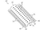
- FIG. 15 is a perspective view illustrating an appearance of the relay terminal member according to the second embodiment.
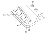
- FIG. 16 is an enlarged perspective view showing a part of FIG.
- the relay terminal member 20 has a flat plate shape as a whole.
- the hole 30 and the opening 27 in the relay terminal member 20 are provided. Is formed in a plate shape having a level difference higher than that of both side portions 42 where the opening grooves 32 and the terminal portions 25 are formed.
- the terminal pin 14 of the connector 12 is inserted and connected to the opening 27 of the relay terminal 21, and its tip is separated from the surface of the circuit board 11.
- the main body 24 of the relay terminal 21 has a crank-like cross section.
- the terminal portion 25 of the relay terminal 21 is formed in a flat plate shape slightly inclined downward, and is soldered to the terminal of the circuit board 11.
- FIG. 17 is a perspective view showing an appearance of the relay terminal before cutting in the second embodiment.
- FIG. 18 is a perspective view showing the relay terminal member connected to the circuit board in the second embodiment.
- the circuit structure 10 and the relay terminal member 20 of the second embodiment are manufactured in the same manner as in the first embodiment. That is, the aggregate 33 of the relay terminals 21 is formed in a stepped shape by pressing. An opening portion 27 is formed in the aggregate 33, and the terminal portions 25 are integrally connected by a connecting portion 34.
- the covering portion 22 having the opening groove 32 and the hole portion 30 is formed in a step shape by injection molding.
- both the side portions of the assembly 33 covered with the covering portion 22 are cut and removed from the connecting portions 34, and the terminal portions 25 are slightly inclined.
- the relay terminal member 20 is manufactured by the above process.
- cream solder is applied to a plurality of terminals on the circuit board 11, and the terminal portions 25 of the relay terminal member 20 are placed on the cream solder as shown in FIG. Subsequently, the relay terminal member 20 and the circuit board 11 are moved into a high-temperature furnace and heated, whereby the plurality of terminal portions 25 of the relay terminal member 20 are soldered to the plurality of terminals on the circuit board 11, respectively.
- the connector 12 is connected to the relay terminal member 20.
- the plurality of terminal pins 14 of the connector 12 are respectively inserted into the openings 27 in the holes 30 in the relay terminal member 20.
- the terminal pin 14 is electrically connected to the relay terminal 21 at the bent convex portion 29.
- the protruding length of the relay terminal member 20 toward the back surface is shorter than the gap A.
- the circuit structure 10 is manufactured through the above steps.
- the relay terminal member 20 includes the terminal portion 25 connected to the circuit board 11 and the main body portion 24 in which the opening portion 27 into which the terminal pin 14 is inserted and connected is formed. Since the relay terminal 21 is provided, the same effect as in the first embodiment can be obtained.
- the tip portion of the terminal pin 14 inserted into the opening 27 is connected to the circuit. It is possible to dispose in the gap A without penetrating the back surface side of the substrate 11. Therefore, the back side of the circuit board 11 can be used more effectively.
- the opening 27 has a shape having four cut portions 28.
- the shape of the opening 27 is not limited to this, and the shape has a number of cut portions 28 other than four.
- it may be another shape such as a circle, an ellipse, a polygon such as a triangle or a rectangle having an inner diameter smaller than that of the hole 30 of the covering portion 22.
- it may be formed so that a plurality of thin slits intersect.
- the present invention is useful for the relay terminal member, the circuit structure including the relay terminal member, and the electronic unit.
Landscapes
- Physics & Mathematics (AREA)
- Thermal Sciences (AREA)
- Engineering & Computer Science (AREA)
- Microelectronics & Electronic Packaging (AREA)
- Coupling Device And Connection With Printed Circuit (AREA)
Priority Applications (3)
| Application Number | Priority Date | Filing Date | Title |
|---|---|---|---|
| CN2009801301323A CN102113183B (zh) | 2008-08-09 | 2009-07-21 | 中继端子部件和包括它的电路结构体以及电子单元 |
| EP09806551A EP2312703A4 (de) | 2008-08-09 | 2009-07-21 | Relaisklemmenelement, schaltkreisstruktur damit und elektronisches gerät |
| US13/058,184 US8513523B2 (en) | 2008-08-09 | 2009-07-21 | Relay terminal member, circuit structure including the same, and electronic unit |
Applications Claiming Priority (2)
| Application Number | Priority Date | Filing Date | Title |
|---|---|---|---|
| JP2008-206469 | 2008-08-09 | ||
| JP2008206469A JP5255365B2 (ja) | 2008-08-09 | 2008-08-09 | 中継端子部材及びそれを備えた回路構造体、並びに電子ユニット |
Publications (1)
| Publication Number | Publication Date |
|---|---|
| WO2010018655A1 true WO2010018655A1 (ja) | 2010-02-18 |
Family
ID=41668809
Family Applications (1)
| Application Number | Title | Priority Date | Filing Date |
|---|---|---|---|
| PCT/JP2009/003408 Ceased WO2010018655A1 (ja) | 2008-08-09 | 2009-07-21 | 中継端子部材及びそれを備えた回路構造体、並びに電子ユニット |
Country Status (6)
| Country | Link |
|---|---|
| US (1) | US8513523B2 (de) |
| EP (1) | EP2312703A4 (de) |
| JP (1) | JP5255365B2 (de) |
| KR (1) | KR20110039375A (de) |
| CN (1) | CN102113183B (de) |
| WO (1) | WO2010018655A1 (de) |
Cited By (1)
| Publication number | Priority date | Publication date | Assignee | Title |
|---|---|---|---|---|
| CN110521063A (zh) * | 2017-04-11 | 2019-11-29 | 罗伯特·博世有限公司 | 电触头装置 |
Families Citing this family (10)
| Publication number | Priority date | Publication date | Assignee | Title |
|---|---|---|---|---|
| DE102011085924A1 (de) * | 2011-11-08 | 2013-05-08 | Robert Bosch Gmbh | Elektrisches Steuergerät für ein Kraftfahrzeug |
| JP6090930B2 (ja) * | 2013-09-17 | 2017-03-08 | 日本航空電子工業株式会社 | コネクタ |
| JP6199220B2 (ja) * | 2014-03-26 | 2017-09-20 | 日本航空電子工業株式会社 | 薄型コネクタ |
| JP6256364B2 (ja) * | 2015-02-03 | 2018-01-10 | 株式会社オートネットワーク技術研究所 | 回路構成体 |
| JP6520179B2 (ja) * | 2015-02-13 | 2019-05-29 | 日本電産リード株式会社 | 中継コネクタ、及び基板検査装置 |
| DE102017109034B4 (de) | 2017-04-27 | 2021-11-11 | Te Connectivity Germany Gmbh | Steckverbindung, elektrischer Stecker und Verfahren zur Herstellung einer elektrischen Verbindung |
| JP7135999B2 (ja) * | 2019-05-13 | 2022-09-13 | 株式会社オートネットワーク技術研究所 | 配線基板 |
| KR102772341B1 (ko) * | 2019-08-14 | 2025-02-25 | 현대자동차주식회사 | 릴레이 |
| JP7523748B2 (ja) | 2020-09-23 | 2024-07-29 | 株式会社リコー | 基板ユニット、着脱ユニット、及び、画像形成装置 |
| KR102940930B1 (ko) * | 2024-01-03 | 2026-03-17 | 주식회사 현대케피코 | 전자 제어 장치용 커넥터 |
Citations (4)
| Publication number | Priority date | Publication date | Assignee | Title |
|---|---|---|---|---|
| JPH04162377A (ja) * | 1990-10-26 | 1992-06-05 | Matsushita Electric Ind Co Ltd | 金属ベース回路基板と外部リード線との接続端子 |
| JP2007048566A (ja) * | 2005-08-09 | 2007-02-22 | Jst Mfg Co Ltd | 締結具及びこの締結具を用いたコネクタ |
| JP2007087748A (ja) | 2005-09-21 | 2007-04-05 | Auto Network Gijutsu Kenkyusho:Kk | 表面実装コネクタ |
| JP2007165084A (ja) | 2005-12-13 | 2007-06-28 | Auto Network Gijutsu Kenkyusho:Kk | 表面実装コネクタ |
Family Cites Families (9)
| Publication number | Priority date | Publication date | Assignee | Title |
|---|---|---|---|---|
| US3874759A (en) * | 1973-10-09 | 1975-04-01 | Jospeh G Colombo | Electrical connector socket for integrated circuit |
| JPH0748566A (ja) | 1993-08-04 | 1995-02-21 | Toray Ind Inc | フォトクロミック材料 |
| JP3043929B2 (ja) | 1993-09-20 | 2000-05-22 | 株式会社東芝 | 共振形インバータ装置 |
| JP2706419B2 (ja) | 1993-12-17 | 1998-01-28 | 泉自動車株式会社 | ウレタンハンドルの成形方法 |
| JP4112475B2 (ja) * | 2003-10-31 | 2008-07-02 | 日本圧着端子製造株式会社 | タインプレート |
| WO2005096683A1 (ja) * | 2004-03-31 | 2005-10-13 | Mitsubishi Cable Industries, Ltd. | 回路基板及びその製造方法及び回路基板を用いたジョイントボックス |
| DE102005027852A1 (de) * | 2005-06-16 | 2006-12-21 | Robert Bosch Gmbh | Anordnung und Verfahren zum elektrischen Anschluss einer elektronischen Schaltung in einem Gehäuse |
| US7722398B2 (en) * | 2007-04-13 | 2010-05-25 | Hon Hai Precision Ind. Co., Ltd. | Electrical connector assembly with a protecting section over a flexible printed circuit board connected thereto |
| CN201041912Y (zh) | 2007-04-13 | 2008-03-26 | 富士康(昆山)电脑接插件有限公司 | 电连接器组件 |
-
2008
- 2008-08-09 JP JP2008206469A patent/JP5255365B2/ja active Active
-
2009
- 2009-07-21 CN CN2009801301323A patent/CN102113183B/zh not_active Expired - Fee Related
- 2009-07-21 WO PCT/JP2009/003408 patent/WO2010018655A1/ja not_active Ceased
- 2009-07-21 US US13/058,184 patent/US8513523B2/en not_active Expired - Fee Related
- 2009-07-21 KR KR1020117004999A patent/KR20110039375A/ko not_active Ceased
- 2009-07-21 EP EP09806551A patent/EP2312703A4/de not_active Withdrawn
Patent Citations (4)
| Publication number | Priority date | Publication date | Assignee | Title |
|---|---|---|---|---|
| JPH04162377A (ja) * | 1990-10-26 | 1992-06-05 | Matsushita Electric Ind Co Ltd | 金属ベース回路基板と外部リード線との接続端子 |
| JP2007048566A (ja) * | 2005-08-09 | 2007-02-22 | Jst Mfg Co Ltd | 締結具及びこの締結具を用いたコネクタ |
| JP2007087748A (ja) | 2005-09-21 | 2007-04-05 | Auto Network Gijutsu Kenkyusho:Kk | 表面実装コネクタ |
| JP2007165084A (ja) | 2005-12-13 | 2007-06-28 | Auto Network Gijutsu Kenkyusho:Kk | 表面実装コネクタ |
Non-Patent Citations (1)
| Title |
|---|
| See also references of EP2312703A4 * |
Cited By (3)
| Publication number | Priority date | Publication date | Assignee | Title |
|---|---|---|---|---|
| CN110521063A (zh) * | 2017-04-11 | 2019-11-29 | 罗伯特·博世有限公司 | 电触头装置 |
| US10873141B2 (en) | 2017-04-11 | 2020-12-22 | Robert Bosch Gmbh | Electrical contact assembly |
| CN110521063B (zh) * | 2017-04-11 | 2021-09-07 | 罗伯特·博世有限公司 | 电触头装置 |
Also Published As
| Publication number | Publication date |
|---|---|
| KR20110039375A (ko) | 2011-04-15 |
| US20110139504A1 (en) | 2011-06-16 |
| CN102113183B (zh) | 2013-07-03 |
| EP2312703A1 (de) | 2011-04-20 |
| EP2312703A4 (de) | 2012-12-12 |
| JP2010044884A (ja) | 2010-02-25 |
| CN102113183A (zh) | 2011-06-29 |
| US8513523B2 (en) | 2013-08-20 |
| JP5255365B2 (ja) | 2013-08-07 |
Similar Documents
| Publication | Publication Date | Title |
|---|---|---|
| JP5255365B2 (ja) | 中継端子部材及びそれを備えた回路構造体、並びに電子ユニット | |
| US6702594B2 (en) | Electrical contact for retaining solder preform | |
| EP2088840B1 (de) | Elektronische Bauteileinheit | |
| KR960010739B1 (ko) | 인쇄 회로 기판의 제조 방법 및 인쇄 회로 기판 조립체 | |
| JP7341943B2 (ja) | 電気コネクタ | |
| CN101345226B (zh) | Ic器件和制造该ic器件的方法 | |
| CN100338824C (zh) | 具有bga连接的印刷电路板组件 | |
| EP0654184B1 (de) | Verbindervorrichtung und verfahren zu seiner herstellung | |
| JP2013065470A (ja) | 電気コネクタ | |
| CN101291565A (zh) | 印刷布线板 | |
| KR100700239B1 (ko) | 인쇄 회로 기판과 케이블의 접속 방법 및 그 방법에 따라 인쇄 회로 기판과 접속된 케이블을 갖는 하우징 | |
| JP5193109B2 (ja) | 回路基板用コネクタ及びその製造方法 | |
| CN101304128B (zh) | 连接孔用电连接端子及具备该端子的电子部件的卡止构造 | |
| JP2003243087A (ja) | コネクタ一体型電子機器 | |
| KR102804340B1 (ko) | 플러그 커넥터 | |
| KR200465414Y1 (ko) | 기판실장형 커넥터 | |
| KR100430140B1 (ko) | 전기 커플링의 열팽창 제어 | |
| CN222422457U (zh) | 电连接器 | |
| US7142083B2 (en) | Electronics component and method for fabricating same | |
| JP2023146592A (ja) | 電子装置 | |
| JP2005135765A (ja) | 電子部品組付体および電子部品組付体の組付け方法 | |
| JP2006049170A (ja) | タインプレート付き基板コネクタ | |
| JP2002299541A (ja) | 表面実装用電源装置におけるリード | |
| KR100721316B1 (ko) | 인쇄회로기판용 커넥터 핀 | |
| JP2003017164A (ja) | コネクタ及びその実装方法 |
Legal Events
| Date | Code | Title | Description |
|---|---|---|---|
| WWE | Wipo information: entry into national phase |
Ref document number: 200980130132.3 Country of ref document: CN |
|
| 121 | Ep: the epo has been informed by wipo that ep was designated in this application |
Ref document number: 09806551 Country of ref document: EP Kind code of ref document: A1 |
|
| REEP | Request for entry into the european phase |
Ref document number: 2009806551 Country of ref document: EP |
|
| WWE | Wipo information: entry into national phase |
Ref document number: 13058184 Country of ref document: US Ref document number: 2009806551 Country of ref document: EP |
|
| NENP | Non-entry into the national phase |
Ref country code: DE |
|
| ENP | Entry into the national phase |
Ref document number: 20117004999 Country of ref document: KR Kind code of ref document: A |