WO2010061550A1 - Esd保護デバイス及びその製造方法 - Google Patents
Esd保護デバイス及びその製造方法 Download PDFInfo
- Publication number
- WO2010061550A1 WO2010061550A1 PCT/JP2009/006199 JP2009006199W WO2010061550A1 WO 2010061550 A1 WO2010061550 A1 WO 2010061550A1 JP 2009006199 W JP2009006199 W JP 2009006199W WO 2010061550 A1 WO2010061550 A1 WO 2010061550A1
- Authority
- WO
- WIPO (PCT)
- Prior art keywords
- insulating layer
- esd protection
- protection device
- auxiliary electrode
- cavity
- Prior art date
- Legal status (The legal status is an assumption and is not a legal conclusion. Google has not performed a legal analysis and makes no representation as to the accuracy of the status listed.)
- Ceased
Links
Images

















Classifications
-
- H—ELECTRICITY
- H01—ELECTRIC ELEMENTS
- H01T—SPARK GAPS; OVERVOLTAGE ARRESTERS USING SPARK GAPS; SPARKING PLUGS; CORONA DEVICES; GENERATING IONS TO BE INTRODUCED INTO NON-ENCLOSED GASES
- H01T4/00—Overvoltage arresters using spark gaps
- H01T4/10—Overvoltage arresters using spark gaps having a single gap or a plurality of gaps in parallel
- H01T4/12—Overvoltage arresters using spark gaps having a single gap or a plurality of gaps in parallel hermetically sealed
-
- H—ELECTRICITY
- H02—GENERATION; CONVERSION OR DISTRIBUTION OF ELECTRIC POWER
- H02H—EMERGENCY PROTECTIVE CIRCUIT ARRANGEMENTS
- H02H9/00—Emergency protective circuit arrangements for limiting excess current or voltage without disconnection
- H02H9/04—Emergency protective circuit arrangements for limiting excess current or voltage without disconnection responsive to excess voltage
-
- H—ELECTRICITY
- H01—ELECTRIC ELEMENTS
- H01T—SPARK GAPS; OVERVOLTAGE ARRESTERS USING SPARK GAPS; SPARKING PLUGS; CORONA DEVICES; GENERATING IONS TO BE INTRODUCED INTO NON-ENCLOSED GASES
- H01T21/00—Apparatus or processes specially adapted for the manufacture or maintenance of spark gaps or sparking plugs
-
- H—ELECTRICITY
- H01—ELECTRIC ELEMENTS
- H01T—SPARK GAPS; OVERVOLTAGE ARRESTERS USING SPARK GAPS; SPARKING PLUGS; CORONA DEVICES; GENERATING IONS TO BE INTRODUCED INTO NON-ENCLOSED GASES
- H01T4/00—Overvoltage arresters using spark gaps
- H01T4/10—Overvoltage arresters using spark gaps having a single gap or a plurality of gaps in parallel
-
- H—ELECTRICITY
- H02—GENERATION; CONVERSION OR DISTRIBUTION OF ELECTRIC POWER
- H02H—EMERGENCY PROTECTIVE CIRCUIT ARRANGEMENTS
- H02H9/00—Emergency protective circuit arrangements for limiting excess current or voltage without disconnection
- H02H9/04—Emergency protective circuit arrangements for limiting excess current or voltage without disconnection responsive to excess voltage
- H02H9/044—Physical layout, materials not provided for elsewhere
-
- H—ELECTRICITY
- H05—ELECTRIC TECHNIQUES NOT OTHERWISE PROVIDED FOR
- H05K—PRINTED CIRCUITS; CASINGS OR CONSTRUCTIONAL DETAILS OF ELECTRIC APPARATUS; MANUFACTURE OF ASSEMBLAGES OF ELECTRICAL COMPONENTS
- H05K9/00—Screening of apparatus or components against electric or magnetic fields
- H05K9/0067—Devices for protecting against damage from electrostatic discharge
-
- H—ELECTRICITY
- H05—ELECTRIC TECHNIQUES NOT OTHERWISE PROVIDED FOR
- H05K—PRINTED CIRCUITS; CASINGS OR CONSTRUCTIONAL DETAILS OF ELECTRIC APPARATUS; MANUFACTURE OF ASSEMBLAGES OF ELECTRICAL COMPONENTS
- H05K9/00—Screening of apparatus or components against electric or magnetic fields
- H05K9/0069—Methods for measuring the shielding efficiency; Apparatus therefor; Isolation container for testing
-
- H—ELECTRICITY
- H05—ELECTRIC TECHNIQUES NOT OTHERWISE PROVIDED FOR
- H05K—PRINTED CIRCUITS; CASINGS OR CONSTRUCTIONAL DETAILS OF ELECTRIC APPARATUS; MANUFACTURE OF ASSEMBLAGES OF ELECTRICAL COMPONENTS
- H05K9/00—Screening of apparatus or components against electric or magnetic fields
- H05K9/0073—Shielding materials
- H05K9/0079—Electrostatic discharge protection, e.g. ESD treated surface for rapid dissipation of charges
-
- H—ELECTRICITY
- H01—ELECTRIC ELEMENTS
- H01B—CABLES; CONDUCTORS; INSULATORS; SELECTION OF MATERIALS FOR THEIR CONDUCTIVE, INSULATING OR DIELECTRIC PROPERTIES
- H01B1/00—Conductors or conductive bodies characterised by the conductive materials; Selection of materials as conductors
- H01B1/20—Conductive material dispersed in non-conductive organic material
-
- Y—GENERAL TAGGING OF NEW TECHNOLOGICAL DEVELOPMENTS; GENERAL TAGGING OF CROSS-SECTIONAL TECHNOLOGIES SPANNING OVER SEVERAL SECTIONS OF THE IPC; TECHNICAL SUBJECTS COVERED BY FORMER USPC CROSS-REFERENCE ART COLLECTIONS [XRACs] AND DIGESTS
- Y10—TECHNICAL SUBJECTS COVERED BY FORMER USPC
- Y10T—TECHNICAL SUBJECTS COVERED BY FORMER US CLASSIFICATION
- Y10T29/00—Metal working
- Y10T29/49—Method of mechanical manufacture
- Y10T29/49002—Electrical device making
Definitions
- the present invention relates to an ESD protection device and a method for manufacturing the same, and more particularly, to improve ESD characteristics such as a discharge start voltage and reliability of an ESD protection device in which discharge electrodes are arranged to face each other in a cavity of an insulating substrate. Regarding technology.
- ESD Electro-Static Discharge
- An ESD protection device is used for such an application, and is also called a surge absorbing element or a surge absorber.
- the ESD protection device is disposed, for example, between the signal line of the circuit and the ground (ground). Since the ESD protection device has a structure in which a pair of discharge electrodes are spaced apart from each other, the ESD protection device has a high resistance in a normal use state, and a signal does not flow to the ground side. On the other hand, when an excessive voltage is applied, for example, when static electricity is applied from an antenna such as a mobile phone, a discharge occurs between the discharge electrodes of the ESD protection device, and the static electricity can be guided to the ground side. Thereby, a voltage due to static electricity is not applied to a circuit subsequent to the ESD device, and the circuit can be protected.
- the ESD protection device shown in the exploded perspective view of FIG. 37 and the cross-sectional view of FIG. 38 is a discharge electrode in which a cavity 5 is formed in a ceramic multilayer substrate 7 on which an insulating ceramic sheet 2 is laminated and is electrically connected to an external electrode 1.
- 6 is disposed oppositely in the cavity 5, and the discharge gas is confined in the cavity 5.
- a voltage causing dielectric breakdown is applied between the discharge electrodes 6, a discharge occurs between the discharge electrodes 6 in the cavity 5, and an excessive voltage is guided to the ground by the discharge, thereby protecting the subsequent circuit.
- discharge responsiveness (ESD responsiveness) to ESD is likely to vary due to variations in the spacing between the discharge electrodes.
- ESD responsiveness is difficult to implement
- the first problem to be solved by the present invention is to provide an ESD protection device that can easily adjust and stabilize the ESD characteristics, and a method for manufacturing the same, in view of such circumstances.
- the second problem to be solved by the present invention is that an ESD protection device capable of easily adjusting and stabilizing the ESD characteristics and preventing the deterioration of the discharge characteristics due to repeated discharges, and its It is to provide a manufacturing method.
- the discharge start voltage is set mainly by adjusting the interval between the discharge electrodes.
- the discharge electrode spacing varies, and the discharge start voltage of the ESD protection device tends to vary. Therefore, the discharge start voltage cannot be set with high accuracy.
- the discharge electrode in the cavity part is caused by a decrease in the airtightness of the cavity part or a difference in thermal expansion coefficient (also referred to as “thermal expansion coefficient”) between the base material layer of the ceramic multilayer substrate and the discharge electrode. , May peel from the ceramic multilayer substrate.
- the device does not function as an ESD protection device, or the discharge start voltage changes, and the reliability of the ESD protection device decreases.
- the third problem to be solved by the present invention is to provide a highly reliable ESD protection device and a method for manufacturing the same, in which the discharge start voltage can be set with high accuracy in view of such a situation.
- the present invention provides an ESD protection device configured as follows.
- the ESD protection device has at least a pair of (a) an insulating substrate, (b) a cavity formed inside the insulating substrate, and (c) an exposed portion that is exposed and opposed to the cavity.
- a conductive powdery auxiliary electrode material is dispersed between the exposed portions of the discharge electrode in the cavity.
- ESD characteristics discharge start voltage, etc.
- discharge start voltage discharge start voltage
- the auxiliary electrode material is covered with an insulating material.
- auxiliary electrode material is covered with the insulating material, it is possible to prevent a short circuit from occurring between the discharge electrodes due to the contact between the adjacent auxiliary electrode materials.
- the discharge phenomenon in the cavity is likely to generate creeping discharge that occurs on the creeping surface between the insulator and the space.
- the auxiliary electrode material By covering the auxiliary electrode material with an insulating material, more creepage surfaces can be formed in the cavity, so that ESD response can be further improved.
- an insulating material is dispersed in the cavity.
- the contact between the auxiliary electrode materials is prevented by the insulating material dispersed in the cavity. Therefore, it is possible to prevent a short circuit from occurring between the discharge electrodes due to contact between adjacent auxiliary electrode materials.
- the insulating substrate is a ceramic substrate.
- the ceramic substrate contains a glass component. Between the ceramic substrate and the cavity, the glass component in the ceramic substrate penetrates into the cavity.
- the sealing member can prevent the glass component in the ceramic substrate from penetrating into the cavity, it is possible to prevent the auxiliary electrode material in the cavity from being necked by the glass component that has penetrated into the cavity. Can do.
- the glass component that has penetrated into the cavity is prevented from eroding the insulating material covering the auxiliary electrode material or the insulating material dispersed between the auxiliary electrode materials, thereby reducing the insulation between the discharge electrodes. Can do.
- the auxiliary electrode material is a conductive material dispersed between the discharge electrodes in the cavity, and the conductive material includes a bottom surface and a ceiling that form the cavity. It touches the surface.
- the ESD response can be further improved compared to the case where the conductive material is dispersed only on one side. Can do.
- the conductive material is in contact with the bottom surface and the top surface forming the cavity, the conductive material is prevented from being detached from the substrate body. Therefore, it is possible to suppress degradation of ESD characteristics (for example, increase in discharge start voltage) due to repeated discharge phenomena.
- a part of the conductive material is embedded in the insulating substrate.
- the conductive material is not only in contact with the insulating substrate but is embedded, the detachment of the conductive material from the insulating substrate can be more effectively suppressed.
- the insulating substrate is a ceramic substrate including a ceramic material and a glass material.
- the conductive material is fixed to the insulating substrate by the glass material.
- the conductive material is not only in contact with the insulating substrate, but is fixed by the glass material, the separation of the conductive material from the insulating substrate can be more effectively suppressed.
- the surface roughness of the inner peripheral surface forming the cavity is reduced. Therefore, the distance traveled by electrons during creeping discharge is shortened, and the ESD response can be further improved.
- the powder of the conductive material that is the auxiliary electrode material is arranged in the thickness direction along the inner surface that forms the cavity between the exposed portions of the discharge electrode.
- An auxiliary electrode portion is formed which is arranged in a single layer containing only one conductive material powder particle.
- the conductive material powder of the auxiliary electrode portion is disposed so as to recede from the inner surface forming the cavity and is not exposed at all in the cavity. There may be a portion that protrudes and is exposed in the cavity.
- the conductive material powder of the auxiliary electrode portion may be arranged at a uniform density, for example, arranged in a single or a plurality of rows of strips, meshes, dots, etc., with different densities. May be.
- the discharge start voltage can be set to a desired value by adjusting the amount and type of the conductive material of the auxiliary electrode portion.
- the discharge start voltage can be set with higher accuracy than the case where the discharge start voltage is adjusted only by changing the interval between the facing portions of the discharge electrode. Since the conductive material powder of the discharge electrode is arranged in a layer including only one conductive material powder particle in the thickness direction, the probability of contact between the conductive material powder of the discharge electrode decreases, Generation
- the contraction behavior and thermal expansion coefficient of the discharge electrode in the region between the discharge electrodes can be reduced.
- the difference can be mitigated.
- At least a part of the powder of the conductive material of the auxiliary electrode part is exposed in the cavity from the inner surface forming the cavity.
- the creeping discharge is further promoted, and the ESD characteristics are improved, such as the reduction of the discharge start voltage and the improvement of the ESD response.
- the conductive material powder of the auxiliary electrode portion is coated with a non-conductive material.
- the auxiliary electrode portion includes a portion formed along an interface between the insulating substrate and the discharge electrode.
- the alignment accuracy between the auxiliary electrode portion and the discharge electrode can be relaxed, and the discharge start voltage can be reduced. Variations are also reduced and manufacturing costs can be reduced.
- the insulating substrate is a ceramic substrate.
- the auxiliary electrode portion is formed along the inner surface of the cavity portion using a conductive material whose shrinkage behavior during firing is the same as or similar to the material of the discharge electrode, so that between the exposed portions of the discharge electrode. In the vicinity of the region, the difference in shrinkage behavior between the discharge electrode and the ceramic substrate can be reduced. As a result, it is possible to reduce defects and characteristic variations caused by peeling of the discharge electrode during firing. In addition, since the variation in the interval between the discharge electrodes is reduced, the variation in the discharge start voltage can be reduced.
- the coefficient of thermal expansion near the auxiliary electrode portion can be set to an intermediate value between the coefficient of thermal expansion of the discharge electrode and the coefficient of thermal expansion of the ceramic substrate.
- the present invention provides a method for manufacturing an ESD protection device configured as follows.
- a method for manufacturing an ESD protection device includes: (i) forming at least a pair of discharge electrodes with an interval provided on at least one of one main surface of the first insulating layer and one main surface of the second insulating layer; And (ii) a state in which a conductive auxiliary electrode material is dispersed between the one discharge electrode between the one main surface of the first insulating layer and the one main surface of the second insulating layer. And (iii) the first insulating layer with the one main surface of the first insulating layer and the one main surface of the second insulating layer facing each other.
- the present invention provides a method for manufacturing an ESD protection device configured as follows.
- the manufacturing method of the ESD protection device includes (i) a first step in which a conductive material is dispersedly attached to one main surface of the first insulating layer, and (ii) the one of the first insulating layers. Forming at least a pair of discharge electrodes on the main surface with an interval so that at least a part of the conductive material attached to the one main surface of the first insulating layer is exposed between the discharge electrodes; And (iii) the one main surface of the first insulating layer is covered with the second insulating layer, the one main surface of the second insulating layer covers the discharge electrode, and the conductive material. And (iv) a fourth step of forming an external electrode connected to the discharge electrode on the surface of the laminate obtained by the third step. Prepare.
- a cavity is formed between the one main surface of the first insulating layer and the one main surface of the second insulating layer. A part of each of the pair of discharge electrodes is exposed in the cavity.
- the conductive material is in contact with the one main surface of the first insulating layer and the one main surface of the second insulating layer, and a gap is formed between the conductive materials.
- the one main surface of the first insulating layer and the one main surface of the second insulating layer become the top surface and the bottom surface forming the cavity, and the top surface and the bottom surface forming the cavity are electrically conductive.
- a structure in contact with the material can be easily formed.
- the one main surface of the second insulating layer is pressure-bonded to the one main surface of the first insulating layer, so that a part of the conductive material is the first main surface.
- the conductive material is not only in contact with the insulating substrate but is embedded, the detachment of the conductive material from the insulating substrate can be more effectively suppressed.
- the first insulating layer and the second insulating layer are mainly composed of a ceramic material.
- the ESD protection device can be easily manufactured by the same manufacturing method as the ceramic multilayer substrate.
- the step of firing the laminate may be before or after the fourth step.
- the conductive material is embedded in one or both of the first insulating layer and the second insulating layer by shrinking the laminated body in the stacking direction.
- the conductive material can be embedded by utilizing the shrinkage at the time of firing the first insulating layer and the second insulating layer mainly composed of a ceramic material.
- one or both of the first insulating layer and the second insulating layer contains a glass material
- the step of firing the laminated body includes the first main surface of the insulating layer.
- a glass layer is formed of the glass material in a region facing the portion to be the cavity.
- the conductive material can be more firmly fixed to the insulating layer by utilizing the penetration of the glass material.
- the surface roughness of the inner peripheral surface forming the hollow portion is reduced, the distance traveled by electrons during creeping discharge is shortened, and the ESD response can be improved.
- a gap forming material dispersed together with the conductive material is attached to the one main surface of the first insulating layer.
- the voids are formed between the conductive materials by eliminating the void forming material from the laminate obtained in the third step.
- the conductive material and the gap forming material are mixed and adhered to the one main surface of the first insulating layer.
- a mixed material of the charged powder containing the conductive material and the charged powder containing the gap forming material is applied to the one main surface of the first insulating layer by electrophotography. Adhere.
- the uniformly dispersed conductive material and void forming material can be adhered to one main surface of the first insulating layer. Therefore, the interval between the conductive materials can be reliably maintained and a stable ESD response can be realized.
- the content of the charged powder containing the conductive material is 20% or more and 80% or less.
- the content of the chargeable powder containing the conductive material is 20% or more, it is easy to obtain good ESD characteristics with the conductive material.
- the content of the chargeable powder containing the conductive material is 80% or less, it is easy to form a sufficient gap between the conductive materials and prevent a short circuit between the discharge electrodes.
- the present invention provides a method for manufacturing an ESD protection device configured as follows.
- the conductive material powder is disposed on one main surface of the first insulating layer, and the conductive material powder is disposed in a layer including only one conductive material powder particle in the thickness direction.
- a cavity surrounded by the second insulating layer, the discharge electrode, and the exposed region is formed.
- a cavity forming layer containing a disappearing material is formed on at least a part of the auxiliary electrode portion to be exposed between the discharge electrodes in the second step.
- the third step after the second insulating layer is formed also on the cavity forming layer, at least a part of the cavity forming layer is eliminated to form the cavity.
- the auxiliary electrode portion is formed of a conductive material powder disposed in a single layer including only one conductive material powder particle in the thickness direction. It is formed by transferring it upward.
- the auxiliary electrode portion is formed by electrophotography.
- the powder of material is coated with the disappearing material.
- the ESD characteristics of the ESD device can be easily adjusted and stabilized, and deterioration of the discharge characteristics due to repeated discharge can be prevented.
- the discharge start voltage can be set with high accuracy, and a highly reliable ESD protection device can be manufactured.
- Example 1-1 It is an expanded sectional view of a cavity part.
- Example 1-1 It is an image figure after auxiliary electrode formation.
- Example 1-1 It is sectional drawing which shows the manufacturing process of an ESD protection device.
- Example 1-1 It is explanatory drawing of discharge.
- Example 1-1 It is explanatory drawing of a cavity part.
- Example 1-1 It is sectional drawing of an ESD protection device.
- (Modification 1-1) It is an expanded sectional view of a cavity part.
- (Modification 1-1) It is an expanded sectional view of a cavity part.
- Example 1-2 It is an image figure after auxiliary electrode formation.
- Example 1-2 It is an expanded sectional view of a cavity part. (Modification 1-2) It is an image figure after auxiliary electrode formation.
- Example 1-3 It is an image figure after auxiliary electrode formation.
- Example 1-4 It is an exploded sectional view showing a manufacturing process of an ESD protection device.
- Example 1-5) It is sectional drawing of an ESD protection device.
- Comparative Example 1 It is a principal part expanded sectional view of an auxiliary electrode.
- Comparative Example 1 It is explanatory drawing of discharge.
- Comparative Example 1 It is sectional drawing of an ESD protection device.
- Example 2-1 It is a principal part expanded sectional view of an ESD protection device.
- FIG. 2 is a cross-sectional view taken along line AA in FIG.
- Example 2-1 It is sectional drawing of an ESD protection device.
- (Modification 2-1) It is sectional drawing of an ESD protection device.
- (Modification 2-2) It is a graph which shows an ESD characteristic.
- (Example 2-1 and Comparative Example 2) It is a principal part expanded sectional view of a cavity part.
- (Example 2-2) It is sectional drawing of an ESD protection device.
- (Example 2-3) It is sectional drawing which shows the manufacturing process of an ESD protection device.
- (Example 2-4) It is sectional drawing of an ESD protection device.
- (Comparative Example 2) It is a principal part expanded sectional view of an ESD protection device.
- (Comparative Example 2) It is sectional drawing of an ESD protection device.
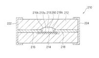
- Example 3-1 It is a principal part expanded sectional view of an auxiliary electrode part.
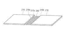
- Example 3-1 It is a perspective view of a discharge electrode and an auxiliary electrode part.
- Example 3-1 It is a principal part expanded sectional view of an auxiliary electrode part.
- (Modification 3-1) It is sectional drawing of an ESD protection device.
- (Example 3-2) It is a principal part expanded sectional view of an auxiliary electrode part.
- (Example 3-2) It is a disassembled perspective view of an ESD protection device.
- Comparative Example 3) It is a principal part expanded sectional view of an auxiliary electrode part.
- Comparative Example 3) It is a disassembled perspective view of an ESD protection device.
- (Conventional example) It is sectional drawing of an ESD protection device. (Conventional example)
- Example 1-1 The ESD protection device 10 of Example 1-1 will be described with reference to FIGS.
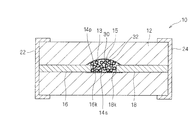
- FIG. 1 is a cross-sectional view of the ESD protection device 10.
- the ESD protection device 10 has a cavity 13 formed inside a substrate body 12 of a ceramic substrate. In the hollow part 13, it arrange
- the discharge electrodes 16 and 18 are formed such that the tips 16k and 18k face each other with a space therebetween.
- the discharge electrodes 16 and 18 extend to the outer peripheral surface of the substrate body 12 and are connected to external electrodes 22 and 24 formed on the surface of the substrate body 12.
- the external electrodes 22 and 24 are used for mounting the ESD protection device 10.
- auxiliary electrode grains 15 in which the surface of a conductive powdery auxiliary electrode material 30 is covered with an insulating material 32 are arranged in the cavity 13. That is, the powdery auxiliary electrode material 30 having conductivity is dispersed in the cavity 13.
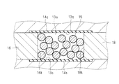
- FIG. 2 is an enlarged cross-sectional view of the cavity 13.
- the top surface 13p and the bottom surface 13s that form the cavity 13 are formed by seal members 14p and 14s.
- the sealing members 14p and 14s extend between the substrate body 12 and the cavity 13 and prevent the glass component in the substrate body 12 that is a ceramic substrate from penetrating into the cavity 13.
- the seal members 14p and 14s have insulating properties.
- Ceramic green sheet A ceramic green sheet for forming the substrate body 12 is produced.
- a material (BAS material) having a composition centered on Ba, Al, and Si is used as the ceramic material.
- Each raw material is prepared and mixed so as to have a predetermined composition, and calcined powder obtained by calcining at 800 ° C. to 1000 ° C. is pulverized for 12 hours with a zirconia ball mill to obtain ceramic powder.
- An organic solvent such as toluene and echinene is added to and mixed with the ceramic powder after calcination of the BAS material.
- a binder and a plasticizer are added and mixed to obtain a slurry.
- the slurry thus obtained is molded onto a PET film by a doctor blade method to obtain a ceramic green sheet having an arbitrary thickness (10 ⁇ m to 50 ⁇ m).
- Electrode paste An electrode paste for forming the discharge electrodes 16 and 18 is prepared.
- An electrode paste is obtained by adding a solvent to a binder resin composed of 80 wt% Cu powder having an average particle diameter of about 2 ⁇ m and ethyl cellulose, and stirring and mixing with a roll.
- the sealing material paste for forming the sealing materials 14p and 14s is produced by the same method as the electrode paste.
- a solvent is added to a binder resin composed of 80% by weight of Al 2 O 3 powder having an average particle size of about 1 ⁇ m and ethyl cellulose, and stirred and mixed with a roll to obtain a seal material paste (alumina paste).
- a seal material paste alumina paste
- As the sealing material a material having a sintering temperature higher than that of the substrate material is selected.
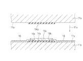
- a sealing material paste (alumina paste) is applied to the surfaces 11p and 11s, which are one main surface of the ceramic green sheets 11a and 11b, by screen printing, and the sealing material 14p , 14s. Since the sealing materials 14p and 14s are arranged so that the ends 16k and 18k of the discharge electrodes 16 and 18 are sandwiched from above and below, they are prepared for two layers.
- Discharge electrode formation Discharge electrodes 16 and 18 are formed by screen printing on the surface 11s of at least one of the ceramic green sheets 11a and 11b on which the sealing materials 14p and 14s are formed.
- the discharge electrodes 16 and 18 are formed in a strip shape so that the width of the discharge electrodes 16 and 18 is 100 ⁇ m and the discharge gap (the distance between the tips 16k and 18k of the opposing discharge electrodes 16 and 18) is 30 ⁇ m. .
- auxiliary electrode formation attachment of auxiliary electrode material
- the surface of the auxiliary electrode material 30 is coated with an insulating material 32 on the ceramic green sheet 11b on which the sealing material 14s and the discharge electrodes 16 and 18 are formed, as shown in FIG.
- auxiliary electrode material Adhesion of auxiliary electrode material by screen printing method
- an auxiliary electrode material is prepared by forming a paste containing the auxiliary electrode material and forming the auxiliary electrode forming layer 15k using the prepared paste. Adhere.
- the paste containing the auxiliary electrode grains 15 is produced by the following method.
- the paste composition is obtained by preparing alumina-coated Cu powder having an average particle size of about 5 ⁇ m at a predetermined ratio, adding a binder resin and a solvent, stirring and mixing with a roll.
- the ratio of resin and solvent in the paste is 40 wt%.
- Alumina-coated Cu powder does not sinter during firing. That is, it does not neck.
- Alumina-coated Cu powder maintains insulation even after firing.
- the height of the cavity 13 can be controlled by controlling the paste application amount.
- the toner is prepared as follows. 1. Alumina-coated Cu powder (average particle size 5 ⁇ m) and a resin are mixed, and the surface of the alumina-coated Cu powder is coated with a resin using a surface treatment machine. 2. Above 1. The sample is classified to remove fine powder and coarse powder. 3. 2. The capsule Cu particles obtained by the above operation and the external additive are mixed, and the external additive is uniformly adhered to the surface of the capsule Cu particles by a surface treatment machine. 4). 3. above. The capsule Cu powder obtained by the above operation and a carrier are mixed to obtain a toner as a developer.
- the auxiliary electrode is formed as follows. 1. The photoreceptor is charged uniformly. 2. The charged photoconductor is irradiated with light to the shape of the auxiliary electrode by an LED to form a latent image. 3. A developing bias is applied to develop the toner on the photoreceptor. The amount of toner applied can be controlled by the magnitude of the developing bias. 4). The photoreceptor on which the pattern of the auxiliary electrode is developed and the ceramic green sheet are overlapped, and the toner is transferred onto the sealing material 14s of the ceramic green sheet 11b. 5. The ceramic green sheet on which the auxiliary electrode pattern is transferred is placed in an oven to fix the toner, thereby obtaining a ceramic green sheet on which the auxiliary electrode pattern is formed.
- auxiliary electrode itself remains insulative after firing.
- the surfaces 11p and 11s of the ceramic green sheets 11a and 11b on which the sealing materials 14p and 14s are formed face each other, and the auxiliary electrodes are formed by the sealing materials 14p and 14s.
- the ceramic green sheets 11a and 11b are stacked so as to sandwich the layer 15k, and are pressed to form a stacked body.
- the ceramic green sheet was laminated so that the thickness of the laminated body was 0.35 mm and the discharge electrode and the auxiliary electrode forming layer were arranged in the center in the thickness direction.
- the temperature range in which the ceramic material is contracted and sintered is fired in a rare gas atmosphere such as Ar and Ne. Good.
- a rare gas atmosphere such as Ar and Ne. Good.
- an air atmosphere may be used.
- electrolytic Ni and Sn plating is performed in the same manner as a chip type component such as an LC filter to complete an ESD protection device.
- an ESD protection device can be easily produced using a ceramic substrate.
- the ceramic material of the substrate main body 12 is not particularly limited to the above-described materials, and may be any insulating material, such as forsterite added with glass, CaZrO 3 added with glass, Others may be used.
- the electrode material of the discharge electrodes 16 and 18 is not limited to Cu, but may be Ag, Pd, Pt, Al, Ni, W, or a combination thereof.
- the auxiliary electrode material 30 is not limited to Cu but may be at least one metal (conductive material) selected from a transition metal group such as Ni, Co, Ag, Pd, Rh, Ru, Au, Pt, and Ir. desirable. Moreover, although these metals may be used alone, they can also be used as alloys. Further, oxides of these metals (resistance materials) may be used. Alternatively, a semiconductor material such as SiC may be used.
- the surface of the auxiliary electrode material 30 is coated with an inorganic material such as Al 2 O 3 , ZrO 2 , or SiO 2 , a mixed calcined material such as BAS, or an farther material 32 such as high melting point glass.
- an inorganic material such as Al 2 O 3 , ZrO 2 , or SiO 2
- a mixed calcined material such as BAS
- an farther material 32 such as high melting point glass.
- the average particle diameter of the auxiliary electrode material 30 is preferably in the range of 0.05 ⁇ m to 10 ⁇ m. A more preferable range is 1 ⁇ m to 5 ⁇ m. The smaller the particle diameter, the larger the surface area, the lower the discharge start voltage, the better the response characteristics to ESD, and the lowering of the discharge characteristics.
- the sealing material 14p, 14s is preferably a ceramic material having a higher sintering temperature than the ceramic used for the substrate body 12. Any insulating material that blocks the glass from the substrate body 12 and does not generate glass itself may be used.
- the discharge start voltage can be reduced and the response characteristics to ESD can be improved.
- the discharge phenomenon between the opposed electrodes is mainly a creeping discharge that runs along the boundary between the cavity (gas phase) and the substrate (insulator) (other discharge phenomena also occur).
- Creeping discharge is a discharge phenomenon in which a current flows through the surface of an object (insulator). Even though electrons flow, it is considered that electrons actually jump on the surface, cause gas ionization, and move. Then, when conductive powder is present on the surface of the insulator, the apparent distance at which electrons jump is shortened to have directionality, and a creeping discharge phenomenon is more actively generated.
- the auxiliary electrode grains 15 in which the surface of the conductive auxiliary electrode material 30 is covered with the insulating material 32 are dispersed and filled between the opposing discharge electrodes 16 and 18. ing.
- the auxiliary electrode material 30 maintains an unsintered state after firing, that is, a state where necking has not occurred.
- Each of the auxiliary electrode grains 15 including the discharge auxiliary material 30 is in a stacked state, that is, in a state of only contacting. As a result, a gap 15y exists between the auxiliary electrode grains 15 as shown in FIG.
- Example 1-1 creeping discharge is generated in the gap between the surface of the stacked auxiliary electrode grains 15, that is, the surface of the insulating material 32 covering the surface of the auxiliary electrode material 30, and the adjacent auxiliary electrode grains 15. Arise.
- Example 1-1 there are many creeping discharge paths as indicated by arrows 82, 84, and 86 in the explanatory diagram of FIG. 5, and therefore creeping discharge is more likely to occur than in Comparative Example 1 described later. That is, the discharge phenomenon can be generated more efficiently. Therefore, the interval between the discharge electrodes 16 and 18 can be reduced, and the fluctuation of the ESD response due to the variation in the interval between the discharge electrodes 16 and 18 can be reduced.
- Example 1-1 since the gap between the auxiliary electrode grains 15 is very small, the loss due to the air discharge is reduced as compared with Comparative Example 1. Therefore, the deterioration of the discharge characteristics can be reduced as compared with Comparative Example 1.
- ESD characteristics discharge start voltage, etc.
- discharge start voltage discharge start voltage
- the presence of the sealing materials 14p and 14s blocks the penetration of the glass component from the ceramic substrate body 12. Therefore, it is possible to prevent the insulating material 32 covering the auxiliary electrode material 30 from being eroded by the glass component and causing the auxiliary electrode material 30 to be sintered, and the auxiliary electrode material 30 itself from being taken into the ceramic of the substrate body 12. As a result, the gap between the auxiliary electrode grains 15 can be maintained, and the ESD protection characteristics can be improved.
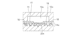
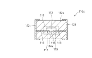
- FIG. 15 is a cross-sectional view of the ESD protection device 10x.
- FIG. 16 is an enlarged cross-sectional view of a main part schematically showing a region 11 indicated by a chain line in FIG.
- FIG. 17 is an explanatory diagram of discharge.
- the cavity 13x is formed inside the substrate body 12x of the ceramic multilayer substrate, and the discharge electrodes 16 and 18 are formed in the cavity 13x. Parts 17 and 19 are exposed.
- the discharge electrodes 16 and 18 are connected to external electrodes 22 and 24 formed on the surface of the substrate body 12x.
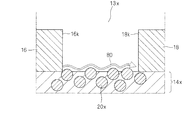
- the ESD protection device 10x differs from the embodiment 1-1 in that an auxiliary electrode 14x is formed adjacent to a portion between the discharge electrodes 16 and 18. As shown in FIG. 16, the auxiliary electrode 14x is a portion where the metal material 20x is dispersed in the insulating material forming the substrate body 12x, and has an insulating property as a whole. A part of the metal material 20x is exposed in the cavity 13x.
- the auxiliary electrode 14x is formed, for example, by applying an auxiliary electrode paste containing a ceramic material and a metal material to a ceramic green sheet.
- the auxiliary electrode forming portion was formed by screen printing.
- the auxiliary electrode was formed by screen printing using a paste containing a metal material.
- the fabrication example of Example 1-1 and the fabrication example of Comparative Example 1 have the same dimensions and shape except for the auxiliary electrode, and the firing conditions are also the same.
- the discharge responsiveness to ESD between the discharge electrodes was evaluated using 100 samples each.
- the discharge response to ESD was performed by an electrostatic discharge immunity test defined in IEC standard, IEC61000-4-2. It was examined whether or not discharge occurred between the discharge electrodes of the sample by applying 2 kV to 8 kv by contact discharge.
- Table 1 The comparison results are shown in Table 1 below.
- Table 1 a circle indicates that a discharge occurred between the discharge electrodes of the sample and the ESD protection function was activated.
- Example 1-1 in which the auxiliary electrode material is dispersed in the cavity, the discharge against ESD is more in comparison with Comparative Example 1 in which the auxiliary electrode in which the metal material is dispersed is formed adjacent to the cavity. It can be seen that the responsiveness is excellent and the ESD protection characteristics can be improved.
- Modified example 1-1 is a modified example of the example 1-1.
- the same reference numerals are used for parts having the same configuration as in the embodiment 1-1, and differences from the embodiment 1-1 will be mainly described.
- FIG. 7 is a cross-sectional view of the ESD protection device 10a of Modification 1-1.
- FIG. 8 is an enlarged cross-sectional view of the main part of the cavity 13a of the ESD protection device 10a of Modification 1-1.
- the height of the cavity 13a in which the auxiliary electrode material is dispersed is about the thickness of the discharge electrodes 16 and 18. . That is, the sealing material 14q that forms the top surface 13q of the cavity 13a extends in a planar shape.
- the surface discharge is most likely to occur at the boundary between the ceramic substrate body 12 and the auxiliary electrode.
- the ESD protection device 10a of the modified example 1-1 since the distance between the boundary portions connecting the discharge electrodes 16 and 18 is reduced by reducing the height of the cavity 13a, the ESD protection characteristics can be further improved.
- Example 1-2 An ESD protection device of Example 1-2 will be described with reference to FIGS. 9 and 10.
- FIG. 9 An ESD protection device of Example 1-2 will be described with reference to FIGS. 9 and 10.
- the ESD protection device of Example 1-2 has substantially the same configuration as the ESD protection device 10 of Example 1-1.
- the same reference numerals are used for the same components as in the embodiment 1-1, and differences from the embodiment 1-1 will be mainly described.
- FIG. 9 is an enlarged cross-sectional view of the main part of the cavity 13.
- insulating particles 15s having insulating properties are dispersed in the cavity portion 13. This is different from the ESD protection device 10 of Example 1-1. That is, the auxiliary electrode is formed by a mixture of the auxiliary electrode particles 15 and the insulating particles 15s.
- the particles 15 and 15s that are disposed in the cavity and form the auxiliary electrode are in an unsintered state and may be in a state where insulation is maintained.
- the auxiliary electrode material contained in the auxiliary electrode grain 15 is preferably at least one metal selected from a transition metal group such as Cu, Ni, Co, Ag, Pd, Rh, Ru, Au, Pt, and Ir. . Moreover, although these metals may be used alone, they can also be used as alloys. Furthermore, oxides of these metals may be used. Alternatively, a semiconductor material such as SiC may be used as the auxiliary electrode material of the auxiliary electrode grains. You may mix and use a metal grain and a semiconductor grain.
- Example 1-2 since the insulating property of the discharge electrode can be ensured by interposing the insulating particles 15 s between the auxiliary electrode particles 15, the auxiliary electrode particles 15 are made of only conductive auxiliary electrode material. You may comprise.
- auxiliary electrode grains in which the surface of the auxiliary electrode material is coated with an insulating material is preferable because the insulation reliability of the discharge electrode is improved.
- the insulating material covering the auxiliary electrode material includes inorganic materials such as Al 2 O 3 , ZrO 2 , SiO 2 , mixed calcined materials such as BAS, and high melting point glass to inhibit sintering of the conductive powder.
- an insulating coating material is used.
- the insulating particles 15s may be anything that does not sinter with the auxiliary electrode particles 15 and does not sinter with the insulating particles 15s.
- an inorganic substance such as ceramic powder (Al 2 O 3 , ZrO 2 , SiO 2, etc.) whose sintering temperature is higher than the firing temperature of the substrate is desirable.
- the ceramic green sheet for forming the substrate body, the electrode paste for forming the discharge electrode, and the sealing material paste for forming the sealing material are the same as in Example 1-1. To make.
- An auxiliary electrode forming layer is formed on a green sheet on which a sealing material and a discharge electrode are formed by a screen printing method or an electrophotographic method.
- a paste containing auxiliary electrode particles and insulating particles is prepared, and the prepared paste is used to assist in the same manner as in Example 1-1.
- An electrode forming layer is formed.
- the paste containing auxiliary electrode grains and insulating grains is prepared by the following method.
- the paste composition is obtained by preparing alumina coated Cu particles and alumina particles having an average particle diameter of about 5 ⁇ m at a predetermined ratio, adding a binder resin and a solvent, stirring and mixing with a roll.
- the volume ratio of the alumina-coated Cu particles and the alumina particles is 1: 1.
- the ratio of resin and solvent in the paste is 40 wt%.
- Alumina-coated Cu powder and alumina particles are not sintered during firing. That is, it does not neck.
- Alumina-coated Cu grains and alumina grains maintain insulation properties both after firing and after firing.
- (B) Discharge auxiliary electrode formation by electrophotography
- a toner containing auxiliary electrode particles and insulating particles is prepared, and the prepared toner is used in Example 1-1.
- An auxiliary electrode forming layer is formed by the same method.
- a toner containing auxiliary electrode grains and insulating grains is prepared as follows. 1. Alumina-coated Cu particles (average particle size 5 ⁇ m) and a resin are mixed, and the surface of the copper powder is coated with a resin using a surface treatment machine. 2. Above 1. The sample is classified to remove fine powder and coarse powder. 3. 2. The capsule Cu particles obtained by the above operation and the external additive are mixed, and the external additive is uniformly adhered to the surface of the capsule Cu particles by a surface treatment machine. 4). 3. above. The developer is obtained by mixing the capsule Cu particles obtained by the above operation and a carrier. 5. The alumina particle toner produced by the same procedure is mixed with the Cu powder toner at a volume ratio of 1: 1.
- Example 1-1 electrolytic Ni and Sn plating is performed on the external electrodes of the fired chip to complete the ESD protection device.
- the ESD protection device of Example 1-2 can improve the ESD protection characteristics by the auxiliary electrode grains 15 as in Example 1-1.
- the insulation reliability of the auxiliary electrode is improved as compared with Example 1-1 by adding insulating particles 15s such as an insulating green ceramic material. .
- Modification 1-2 will be described with reference to FIG.
- Modified example 1-2 is a modified example of the embodiment 1-2.
- the height of the cavity 13a in which the auxiliary electrode grains 15 and the insulating grains 15s are dispersed is as shown in FIG. , 18 or so. That is, the sealing material 14q that forms the top surface 13q of the cavity 13a extends in a planar shape.
- the creeping discharge is most likely to occur at the boundary between the ceramic substrate body 12 and the auxiliary electrodes 16 and 18.
- the distance between the discharge electrodes 16 and 18 is shortened by reducing the height of the cavity 13a, so that creeping discharge is more likely to occur than in the example 1-2. Further improvement in ESD protection characteristics can be obtained.
- Example 1-3 An ESD protection device according to Example 1-3 will be described with reference to FIG.
- the ESD protection device of Example 1-3 has substantially the same configuration as the ESD protection device 10 of Example 1-1.
- the same reference numerals are used for the same components as in the embodiment 1-1, and differences from the embodiment 1-1 will be mainly described.
- FIG. 12 is an image before firing of the cavity where the discharge electrode forming layer is formed.
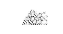
- the disappearing particles 15x that disappear after firing are arranged on the sealing material 14. It differs from the ESD protection device 10 of Example 1-1. That is, the auxiliary electrode forming layer is formed by the mixture of the auxiliary electrode grains 15 and the disappearing grains 15x, and after firing, the auxiliary electrode grains 15 are dispersed in the cavity.
- the ceramic green sheet for forming the substrate body, the electrode paste for forming the discharge electrode, and the sealing material paste for forming the sealing material are the same as in Example 1-1. To make.
- An auxiliary electrode forming layer is formed on a green sheet on which a sealing material and a discharge electrode are formed by a screen printing method or an electrophotographic method.
- (A) Discharge auxiliary electrode formation by screen printing method In the case of screen printing method, a paste containing auxiliary electrode grains and disappearing grains is prepared, and the auxiliary electrode is produced in the same manner as in Example 1-1 using the prepared paste. A forming layer is formed.
- the paste containing the auxiliary electrode grains and the disappearing grains is produced by the following method.
- the paste composition is obtained by preparing alumina-coated Cu particles having an average particle size of about 5 ⁇ m and acrylic resin beads at a predetermined ratio, adding a binder resin and a solvent, stirring and mixing with a roll. 2.
- the volume ratio of Cu particles and acrylic resin beads is 1: 1.
- the ratio of resin and solvent in the paste is 40 wt%. 4).
- Alumina-coated Cu grains are auxiliary electrode grains, and maintain insulating properties after firing and after firing. 5.
- Acrylic resin beads are vanished grains that disappear during firing.
- Example 1 Discharge Auxiliary Electrode Formation by Electrophotography
- a toner containing auxiliary electrode grains and disappearing grains is prepared, and the prepared toner is used to produce Example 1
- the auxiliary electrode forming layer is formed by the same method as in 1.
- a toner containing auxiliary electrode grains, insulating grains, and disappearing grains is prepared as follows. 1. Alumina-coated Cu particles (average particle size 5 ⁇ m) as auxiliary electrode particles and a resin are mixed, and the surface of the copper powder is coated with a resin using a surface treatment machine. 2. Above 1. The sample is classified to remove fines and spices. 3. 2. The capsule Cu particles obtained by the above operation and the external additive are mixed, and the external additive is uniformly adhered to the surface of the capsule Cu particles by a surface treatment machine. 4). 3. above. The capsule Cu particles obtained by the above operation and a carrier are mixed to obtain a toner as a developer. 5. A toner containing acrylic resin beads as vanished particles is prepared in the same procedure, and mixed with toner containing alumina-coated Cu particles at a volume ratio of 1: 1.
- Example 1-1 electrolytic Ni and Sn plating is performed on the external electrodes of the fired chip to complete the ESD protection device.
- the resin beads preferably have an average particle size of 0.05 ⁇ m to 10 ⁇ m, and more preferably 1 ⁇ m to 5 ⁇ m.
- the vanished grains may be carbon or other vanishable grains, even if not vanished.
- the auxiliary electrode forming layer which is a mixture of auxiliary electrode grains and resin beads may be in a state where the arranged particles are in an unsintered state and insulative.
- the auxiliary electrode material contained in the auxiliary electrode grains should be not only Cu but also at least one metal selected from a transition metal group such as Ni, Co, Ag, Pd, Rh, Ru, Au, Pt, and Ir. Is desirable. These metals may be used alone or as an alloy. Furthermore, oxides of these metals may be used. Alternatively, a semiconductor material such as SiC may be used. You may mix and use a metal grain and a semiconductor grain.
- a transition metal group such as Ni, Co, Ag, Pd, Rh, Ru, Au, Pt, and Ir. Is desirable. These metals may be used alone or as an alloy. Furthermore, oxides of these metals may be used. Alternatively, a semiconductor material such as SiC may be used. You may mix and use a metal grain and a semiconductor grain.
- the auxiliary electrode grains may contain only the auxiliary electrode material, but in order to inhibit sintering of the auxiliary electrode material, an inorganic material such as Al 2 O 3 , ZrO 2 , SiO 2 , mixed calcining such as BAS It is more preferable that the auxiliary electrode material is covered with a coating material having an insulating property such as a material or a high melting point glass.
- the ESD protection characteristics can be improved by the auxiliary electrode grains 15 as in Example 1-1.
- the added resin beads inhibit the contact of each particle of the discharge auxiliary electrode and prevent sintering (necking). The insulation reliability of the electrode is improved.
- Example 1-4 will be described with reference to FIG.
- FIG. 13 is an image diagram before firing of the cavity where the discharge electrode forming layer is formed.
- Example 1-4 is different from Examples 1-1 to 1-3 in that the particles are arranged in the cavity.
- Cu particles 15a that are auxiliary electrode particles containing a conductive material, alumina particles 15s that are insulating particles, and acrylic resin beads 15x that are vanishing particles, Are dispersed.
- alumina coated Cu particles 15 which are auxiliary electrode particles whose surface of the conductive material is coated with an insulating material, alumina particles 15s which are insulating particles, Acrylic resin beads 15x which are vanished grains are dispersed.
- SiC particles 15b that are auxiliary electrode grains containing a semiconductor material, alumina grains 15s that are insulating grains, and acrylic resin beads 15x that are disappearing grains, Are dispersed.
- alumina-coated Cu particles 15 which are auxiliary electrode particles whose surface of a conductive material is coated with an insulating material on an alumina sealing material 14 and SiC which are auxiliary electrode particles containing a semiconductor material.
- the particles 15b, the alumina particles 15s that are insulating particles, and the acrylic resin beads 15x are dispersed.
- the auxiliary electrode forming layer on which particles are arranged as shown in FIGS. 13A to 13D can be formed by combining the manufacturing method of Example 1-2 and the manufacturing method of Example 1-3.
- the ESD protection device of Example 1-4 can improve the ESD protection characteristics by the auxiliary electrode grains 15 as in Example 1-1.
- the ESD protection device of Example 4 improves the insulation reliability of the auxiliary electrode compared to Example 1-1 by adding insulating grains.
- the added resin beads inhibit the contact of each particle of the discharge auxiliary electrode and prevent sintering (necking). Insulation reliability is improved.
- Example 1-5 An ESD protection device of Example 1-5 will be described with reference to FIG.
- the ESD protection device of Example 1-5 is different from Examples 1-1 to 1-4 in that the substrate body is a resin substrate.
- Substrate B A substrate B schematically shown in FIG. 14B is produced. That is, the toner 60 containing the auxiliary electrode particles is disposed on the prepreg 11t by electrophotography in the same manner as in Example 1-1.
- the substrate A (fully cured body) and the substrate B (semi-cured body) are stacked and bonded to the substrate A by complete curing of the substrate B.
- a cavity is formed between the tip 16t of the discharge electrode 16a and the tip 18t of the discharge electrode 18a.
- the toner 60 containing auxiliary electrode grains is disposed in the cavity.
- the substrate A and the substrate B may be overlapped and bonded with an adhesive.
- a baked electrode or a conductive resin electrode is formed on the end face of the bonded substrate, and a plating process is performed to form an external electrode.
- the ESD protection characteristics can be improved by the toner 60 containing the auxiliary electrode particles, similarly to the ESD protection device of Example 1-1.
- the sealing material included in the ESD protection device of Example 1-1 is not necessary.
- FIG. 18 is a cross-sectional view of the ESD protection device 110.
- FIG. 19 is an enlarged cross-sectional view of a main part of the cavity 113 of the ESD protection device 110.
- 20 is a cross-sectional view taken along line AA in FIG.
- the ESD protection device 110 has a cavity 113 formed inside a substrate body 112 of a ceramic multilayer substrate. In the hollow part 113, it arrange
- the discharge electrodes 116 and 118 extend to the outer peripheral surface of the substrate body 112 and are connected to external electrodes 122 and 124 formed on the surface of the substrate body 112.
- the external electrodes 122 and 124 are used for mounting the ESD protection device 110.
- the discharge electrodes 116 and 118 are formed such that the tips 116k and 118k exposed in the cavity 113 are opposed to each other with a space therebetween.
- a conductive material 120 is disposed inside the cavity 113.
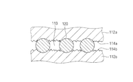
- the conductive material 120 is sandwiched between the top surface 114 a and the bottom surface 114 b that form the cavity 113.
- the conductive material 120 is a powder and is dispersedly arranged. A portion where the conductive material 120 is disposed (hereinafter, also referred to as “auxiliary electrode”) is maintained as a whole.
- the conductive material 120 is preferably made of at least one metal selected from a transition metal group such as Cu, Ni, Co, Ag, Pd, Rh, Ru, Au, Pt, and Ir. Moreover, although these metals may be used alone, they can also be used as alloys. Furthermore, oxides of these metals may be used. Alternatively, a semiconductor material such as SiC may be used.
- a transition metal group such as Cu, Ni, Co, Ag, Pd, Rh, Ru, Au, Pt, and Ir.
- these metals may be used alone, they can also be used as alloys.
- oxides of these metals may be used.
- a semiconductor material such as SiC may be used.
- these metals coated with an inorganic material such as Al 2 O 3 , ZrO 2 , SiO 2 or a mixed calcined material such as a BAS material described in detail later may be used instead of the conductive material 120.
- a material coated with an organic material such as a resin may be used instead of the conductive material 120.
- the ESD protection device 110 when a voltage of a predetermined level or more is applied between the external electrodes 122 and 124, a discharge occurs between the opposing discharge electrodes 116 and 118 in the cavity 113. Since the conductive material 120 is in contact with the top surface 114a and the bottom surface 114b that form the hollow portion 113, electrons easily move and a discharge phenomenon can be generated more efficiently.
- the discharge phenomenon between the discharge electrodes 116 and 118 is caused by the interface between the gas phase of the cavity 113 and the substrate body 112 that is an insulator (that is, the inner peripheral surface including the top surface 114a and the bottom surface 114b forming the cavity 113). ) Is mainly generated. Creeping discharge is a discharge phenomenon in which a current flows through the surface of an object (insulator). Even though electrons flow, it is considered that electrons actually jump on the surface, cause gas ionization, and move. Then, when conductive powder is present on the surface of the insulator, it is presumed that the apparent distance at which electrons jump is shortened to have directionality, and the creeping discharge phenomenon is more actively generated.
- the conductive material 120 since the conductive material 120 is in contact with the top surface 114a and the bottom surface 114b that form the cavity 113, the conductive material 120 does not leave the substrate body 112 due to an impact during discharge. Therefore, the ESD discharge characteristics do not deteriorate after repeated discharge. In addition, since a part of the conductive material 120 is embedded in the insulating layers 112a and 112b of the substrate body 112 as shown in FIG. 19, the detachment of the conductive material 120 is more reliably suppressed.
- the conductive material 120 is in contact with both the top surface 114a and the bottom surface 114b forming the cavity 113, creeping discharge is likely to occur at both the top surface 114a and the bottom surface 114b. Therefore, compared to the case where the conductive material is dispersed only on the bottom surface side as in Comparative Example 2 described later, the area where creeping discharge occurs is doubled and the creeping discharge is more likely to occur. The characteristics can be further improved.
- Ceramic Green Sheet A ceramic green sheet for forming the substrate body 112 is produced as follows.
- a material (BAS material) having a composition centered on Ba, Al, and Si is used as the ceramic material.
- Each raw material is prepared and mixed so as to have a predetermined composition, and calcined powder obtained by calcining at 800 ° C. to 1000 ° C. is pulverized for 12 hours with a zirconia ball mill to obtain ceramic powder.
- An organic solvent such as toluene and echinene is added to and mixed with the ceramic powder after calcination of the BAS material. Further, a binder and a plasticizer are added and mixed to obtain a slurry.
- the slurry thus obtained is molded onto a PET film by a doctor blade method to obtain a ceramic green sheet having a thickness of 50 ⁇ m.
- the ceramic material is not particularly limited to this material and may be any insulating material, so that other materials such as forsterite added with glass and CaZrO 3 added with glass may be used. Good.
- the auxiliary electrode toner which is a chargeable powder containing the conductive material 120 to be disposed in the cavity 113, is produced as follows. 1. Surface copper oxide powder (average particle size 14 ⁇ m) and acrylic resin are mixed and the surface of the copper powder is coated with a surface treatment machine. 2. The fine powder and coarse powder of the sample 1 are cut using a classifier. 3. The composite powder obtained by coating the acrylic resin on the copper surface obtained by the above-mentioned operation 2 is dispersed in an aqueous solution in which a dispersant is dissolved, and after settling, the supernatant is removed and dried in a vacuum drying oven. 4). The composite powder obtained by the above operation 3 and an external additive (silica powder) are mixed, and the external additive is uniformly attached to the surface of the composite powder using a surface treatment machine, thereby obtaining an auxiliary electrode toner.
- an external additive silicon powder
- the conductive material that is a conductive material constituting the auxiliary electrode toner is at least one metal selected from a transition metal group such as Cu, Ni, Co, Ag, Pd, Rh, Ru, Au, Pt, and Ir. Is desirable. Moreover, although these metals may be used alone, they can also be used as alloys. Furthermore, oxides of these metals may be used. Further, a semiconductor material such as SiC or a resistance material may be used.
- the average particle diameter of the auxiliary electrode toner is preferably 3 ⁇ m to 30 ⁇ m. A more preferable average particle diameter is 5 ⁇ m to 20 ⁇ m. When the average particle diameter of the auxiliary electrode toner is 20 ⁇ m or less, it is easy to disperse so as not to cause a short circuit between the discharge electrodes. If the average particle diameter of the auxiliary electrode toner is 5 ⁇ m or more, a sufficient gap between the ceramic layers sandwiching the auxiliary electrode toner from above and below is secured so that the gap between the upper and lower ceramic layers is not filled with glass during firing. Can be.
- the auxiliary electrode toner preferably has a conductive material content of 10 wt% to 95 wt%. A more preferable content is 30 wt% to 70 wt%.
- the content of the conductive material is 95 wt% or less, it is easy to prevent the conductive material from being exposed on the surface due to a shortage of resin in the toner and the chargeability from being deteriorated.
- the content of the conductive material is 10 wt% or more, it is easy to efficiently generate a discharge phenomenon with the auxiliary electrode.
- toner coating resin As a toner coating resin, it has good charging characteristics such as acrylic, styrene allyl, polyolefin, polyester, polypropylene, butyral, etc., and disappears due to combustion, decomposition, melting, vaporization, etc. during firing. It is preferable that the true surface of the conductive material is exposed. However, even if it does not completely disappear, it may remain about 10 nm thick.
- the cavity forming toner which is a chargeable powder for forming a cavity for forming the space of the cavity 113, is a mixture of acrylic beads (average particle size: 15 ⁇ m) and an external additive, and is applied to the surface of the acrylic beads by a surface treatment machine. It is prepared by uniformly attaching an external additive.
- the resin material constituting the cavity-forming toner was selected from acrylic resins, styrene acrylic resins, polyolefin resins, polyester resins, butyral resins, etc. that burn and disappear, or resins that decompose into monomers at high temperatures. It is desirable to use at least one kind of resin. These resins may be used alone or in combination.
- the average particle size of the toner for forming cavities is preferably 3 ⁇ m to 30 ⁇ m.
- a more preferable average particle diameter is 5 ⁇ m to 20 ⁇ m.
- the average particle diameter of the void forming toner is 20 ⁇ m or less, it is easy to prevent a large void from being formed after firing even when the void forming toner is scattered on the background portion other than the pattern.
- the average particle diameter of the cavity forming toner is 5 ⁇ m or more, a sufficient gap between the ceramic layers sandwiching the auxiliary electrode toner from the top and bottom direction may be secured, and the gap between the top and bottom ceramic layers may be filled with glass during firing. Can not be.
- the particle diameter of the cavity forming toner is preferably the same as that of the auxiliary electrode toner.
- the material constituting the cavity forming toner is preferably one that disappears at a temperature (600 to 700 ° C.) or less at which the glass in the ceramic flows. After the void forming toner disappears and the voids are formed, the glass flows to hold the conductive material, and the surface roughness of the creeping surface can be reduced.
- the temperature at which the material constituting the cavity-forming toner disappears is higher than the temperature at which the glass in the ceramic flows (600 to 700 ° C.), the glass that has oozed out of the ceramic layer It can be prevented from filling.
- carbon or the like can be used as the material constituting the void forming toner and disappearing.
- discharge electrode paste The discharge electrode paste for forming the discharge electrodes 116 and 118 is obtained by joining and mixing a sample obtained by adding a solvent to a binder resin composed of 80 wt% Cu powder having an average particle diameter of 2 ⁇ m and ethyl cellulose. To produce.
- the conductive material of the discharge electrode paste is preferably at least one metal selected from a transition metal group such as Cu, Ni, Co, Ag, Pd, Rh, Ru, Au, Pt, and Ir. Moreover, although these metals may be used alone, they can also be used as alloys. Furthermore, oxides of these metals may be used.
- Adhesion of conductive material A conductive material is adhered to the produced ceramic green sheet by electrophotography as follows. 1. The auxiliary electrode toner containing the conductive material and the cavity forming toner are mixed so that the volume ratio is 1: 1. 2. The mixed toner obtained in 1 above and a carrier are mixed to produce a transfer toner. 3. The photoreceptor is charged uniformly. 4). A latent image is formed by irradiating the photosensitive member charged by the LED with light in a pattern of auxiliary electrodes. In the manufacturing example, the pattern of the auxiliary electrode was 30 ⁇ m ⁇ 100 ⁇ m having the same size as the gap between the discharge electrodes. 5. A developing bias is applied to develop the transfer toner on the photoreceptor. 6).
- the photoreceptor on which the pattern of the transfer toner is developed and the ceramic green sheet are overlapped, and the transfer toner is transferred to the ceramic green sheet. 7).
- the ceramic green sheet on which the pattern of the transfer toner is transferred is placed in an oven to fix the toner, and the auxiliary electrode toner containing the conductive material and the cavity forming toner are disposed in the area to be the cavity. Get a sheet.
- the transfer toner which is a uniform mixture of the auxiliary electrode toner containing conductive material and the toner for forming cavities, to the ceramic green sheet, the distance between the conductive materials is reliably maintained and stable ESD response is realized. can do.
- the mixing ratio of the auxiliary electrode toner containing the conductive material and the cavity forming toner is preferably in the range of 10 to 90% by volume. More preferably, the content of the auxiliary electrode toner in the transfer toner is 20 to 80%. When the content of the auxiliary electrode toner in the transfer toner is 20% or more, it is easy to obtain good ESD discharge characteristics with the conductive material (conductive powder). When the content of the auxiliary electrode toner in the transfer toner is 80% or less, it is easy to prevent a short circuit between the discharge electrodes by sufficiently forming a gap between the conductive materials (conductive powder). .
- the size of the pattern of the auxiliary electrode on which the transfer toner is arranged is the same as the gap between the discharge electrodes, but it may be designed to be about 10 ⁇ m to 50 ⁇ m in consideration of printing misalignment. Conversely, the discharge electrode pattern may be larger by about 10 ⁇ m to 50 ⁇ m than the auxiliary electrode pattern on which the transfer toner is disposed.
- a discharge electrode is formed by screen printing. That is, for the ceramic green sheet on which the auxiliary electrode pattern is transferred with the transfer toner, the discharge electrode pattern is formed by screen printing on the surface on which the auxiliary electrode pattern is transferred.
- the discharge electrode was formed to have a thickness of 100 ⁇ m and a discharge gap width (distance between the tips of the discharge electrodes) of 30 ⁇ m.
- the discharge electrode pattern was formed by screen printing, but other well-known wiring pattern forming methods such as electrophotographic printing, ink jet printing, thermal transfer printing, gravure printing, and direct drawing printing can be suitably used.
- Ceramic green sheets are laminated and fired as follows. 1. A pattern of the discharge electrode is formed on the ceramic green sheet of a necessary layer. 2. All layers of ceramic green sheets are laminated and pressure-bonded to form a laminate. 3. Like a chip type component such as an LC filter, the laminate is cut using a mold and divided into chips. In the production example, it was cut to be 1.0 mm ⁇ 0.5 mm. 4). An electrode paste is applied to the end face of the chip to form an external electrode. 5. Firing is performed in an N 2 atmosphere. When a rare gas such as Ar or Ne is introduced into the cavity in order to reduce the voltage against ESD, the temperature region where the ceramic material is contracted and sintered may be fired in a rare gas atmosphere such as Ar or Ne. . In the case of an electrode material (such as Ag) that does not oxidize, an air atmosphere may be used.
- a rare gas such as Ar or Ne
- the height of the cavity becomes about 60-80% of the height of the part corresponding to the cavity before firing. That is, the conductive material is cut into the upper and lower ceramic layers by 20 to 40% of the shrinkage and embedded in the ceramic layers, and the conductive material is held by the ceramic layers.
- Ni and Sn plating is performed on the external electrode to complete the ESD protection device.
- an ESD protection device When an ESD protection device is manufactured using a ceramic substrate as described above, it is easy to form a hollow portion and a conductive material sandwiched and dispersed between the top and bottom surfaces forming the hollow portion.
- a resin is used for the toner for forming a cavity.
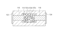
- the width of the region where the conductive material 120 is disposed may be the same as or smaller than the width of the discharge electrode. That is, in the manufacturing example, the conductive material 120 is disposed only in the region 113k where the tips 116k and 118k of the discharge electrodes 116 and 118 shown by the chain line in FIG. 20 are opposed to each other, but as shown in FIG. Even if the conductive material 120 is arranged to the outside, conversely, the conductive material 120 may be arranged only in a part within the chain line region 113k.
- FIG. 27 is a cross-sectional view of the ESD protection device 110x.
- FIG. 28 is an essential part enlarged cross-sectional view schematically showing a region 111 indicated by a chain line in FIG.
- the cavity portion 13 is formed inside the substrate body 112x of the ceramic multilayer substrate, and the discharge electrodes 116, 118 are formed in the cavity portion 113, as in Example 2-1. Part 117,119 is exposed.
- the discharge electrodes 116 and 118 are connected to external electrodes 122 and 124 formed on the surface of the substrate body 112x.
- an auxiliary electrode 114x is formed adjacent to the portion 115 between the discharge electrodes 116 and 118.
- the auxiliary electrode 114x is a portion in which the conductive material 120x is dispersed in the insulating material forming the substrate body 112x, and has an insulating property as a whole. A part of the conductive material 120 x is exposed in the cavity 113.
- the auxiliary electrode 114x is formed, for example, by applying an auxiliary electrode paste containing a ceramic material and a conductive material to the ceramic green sheet.
- a part of the conductive material 120x in the auxiliary electrode 114x may be scattered due to an impact at the time of discharge, and the distribution density of the conductive material 120x may be reduced. For this reason, the discharge voltage gradually increases after repeated discharge, and the ESD discharge characteristics may deteriorate.
- Example 2-1 the discharge voltage (discharge start voltage) in Example 2-1 is lower than that in Comparative Example 2, and that Example 2-1 can improve the ESD discharge characteristics as compared with Comparative Example 2.
- FIG. 21 which is a cross-sectional view similar to FIG. 20, conductive materials 120a, 120b, and 120c having different sizes are mixed and arranged in the cavity 113, and the cavity 113 is formed. It may be sandwiched between the top and bottom surfaces to be formed.
- FIG. 22 which is a cross-sectional view similar to FIG. 20, polygonal conductive materials 120s and 120t are arranged in the cavity 113, and the top surface for forming the cavity 113 and It may be sandwiched between the bottom surfaces.
- Example 2-2 An ESD protection device of Example 2-2 will be described with reference to FIG.
- Example 2-2 has substantially the same configuration as Example 2-1.
- the same reference numerals are used for the same components as in the embodiment 2-1, and the description will focus on the differences from the embodiment 2-1.
- the substrate body of the ESD protection device of Example 2-2 is a ceramic multilayer substrate including a ceramic material and a glass material.
- the glass layers 115a and 115b are formed of a glass material that has leached into the cavity 113p from the insulating layers 112p and 112q of the substrate main body mainly composed of a ceramic material during firing.
- the top surface 114p and the bottom surface 114q of the cavity 113p are formed by the glass layers 115a and 115b.
- the glass layers 115a and 115b are formed to have a desired thickness by adjusting the amount of glass oozing from the ceramic layers 112p and 112q by adjusting the atmosphere (O 2 concentration, H 2 concentration, etc.) during firing. Is possible. If all of the conductive material 120 is covered with glass, the ESD discharge characteristics deteriorate. Therefore, the firing atmosphere is adjusted so that only the upper and lower sides of the conductive material 120 are covered with glass.
- the glass If the glass exudes too much, it fills the cavity and degrades the ESD discharge characteristics. Therefore, it is preferable to secure the height of the cavity to about 5 to 30 ⁇ m.
- various glasses such as borosilicate glass, borosilicate glass, feldspar crystalline glass, cordierite glass, diopside glass, and lanthanoid titanate glass can be used.
- Example 2-2 achieves an effect equal to or greater than that of Example 2-1.
- the ESD responsiveness can be enhanced by the conductive material 120 in contact with the top surface 114p and the bottom surface 114q forming the cavity 113p, the adjustment and stabilization of the ESD characteristics are facilitated.
- the top surface 114p and the bottom surface 114q that form the cavity 113p are formed of the glass layers 115a and 115b, thereby reducing the surface roughness. Therefore, the distance traveled by electrons during creeping discharge is shortened, and the ESD response can be further improved.
- the ESD response can be further improved as compared with the case where the conductive material is dispersed only on one side. it can.
- the conductive material 120 is fixed to the substrate body by the glass layers 115a and 115b. Therefore, the detachment from the substrate body is more effectively suppressed as compared with the case where the conductive material 120 is simply in contact with the substrate body. Therefore, it is possible to further suppress the deterioration of the ESD characteristics (for example, increase in the discharge start voltage) due to the repetition of the discharge phenomenon.
- Example 2-3 An ESD protection device 110a according to Example 2-3 will be described with reference to FIG.
- the aggregates 130, 132, and 134 of the conductive material are sandwiched between the top surface 114s and the bottom surface 114t that form the cavity 113a.
- Aggregates 130, 132, and 134 of conductive material are dispersed in the cavity 113a.
- Example 2-3 The effect similar to that of Example 2-1 can be obtained by Example 2-3.
- the ESD responsiveness can be enhanced by the aggregates 130, 132, and 134 of the conductive material in contact with the top surface 114s and the bottom surface 114t forming the cavity 113a, the adjustment and stabilization of the ESD characteristics can be easily performed. Become.
- the aggregates 130, 132, and 134 of the conductive material are in contact with both the top surface 114s and the bottom surface 114t forming the cavity 113a, compared with the case where the conductive material is dispersed only on one side. ESD responsiveness can be increased.
- the aggregates 130, 132, and 134 of the conductive material are in contact with both the top surface 114s and the bottom surface 114t that form the cavity 113a, separation from the substrate body 112a is prevented. Therefore, it is possible to suppress degradation of ESD characteristics (for example, increase in discharge start voltage) due to repeated discharge phenomena.
- Example 2-4 An ESD protection device of Example 2-4 will be described with reference to FIG.
- the ESD protection device of Example 2-4 is different from Example 2-1 in that the substrate body is formed of resin.
- a chargeable powder containing a conductive material (hereinafter, referred to as “conductive material-containing toner”) 160 is disposed in a dispersed state by electrophotography.
- the substrate A (fully cured body) and the substrate B (semi-cured body) are stacked and bonded to the substrate A by complete curing of the substrate B.
- a cavity is formed between the tip 116t of the discharge electrode 116a and the tip 118t of the discharge electrode 118a.
- the conductive material-containing toner 160 is supported while being sandwiched between the substrate A and the substrate B in the cavity.
- the substrate A and the substrate B may be superposed and bonded with an adhesive.
- a baked electrode or a conductive resin electrode is formed on the end face of the bonded substrate, and a plating process is performed to form an external electrode.
- Example 2-4 the same effect as in Example 2-1 can be obtained.
- the ESD responsiveness can be enhanced by the conductive material-containing toner 160 that is in contact with the top and bottom surfaces (substrate A and substrate B) that form the cavity, it is easy to adjust and stabilize the ESD characteristics. .
- the conductive material-containing toner 160 is in contact with both the top surface and the bottom surface (substrate A and substrate B) that form the cavity, it is more ESD than the case where the conductive material is dispersed only on one side. Responsiveness can be improved.
- the conductive material-containing toner 160 is in contact with both the top surface and the bottom surface (substrate A and substrate B) that form the cavity, separation from the substrate A and the substrate B is prevented. Therefore, it is possible to suppress degradation of ESD characteristics (for example, increase in discharge start voltage) due to repeated discharge phenomena.
- Example 3-1 An ESD protection device 210 according to Example 3-1 will be described with reference to FIGS. 29 to 32.
- FIG. FIG. 29 is a cross-sectional view of the ESD protection device 210.
- the ESD protection device 210 has a cavity 213 formed inside a substrate body 212 of a ceramic multilayer substrate. In the hollow part 213, it arrange
- the discharge electrodes 216 and 218 extend to the outer peripheral surface of the substrate body 212 and are connected to external electrodes 222 and 224 formed on the surface of the substrate body 212.
- the external electrodes 222 and 224 are used for mounting the ESD protection device 210.
- the tips 216k and 218k of the discharge electrodes 216 and 218 are opposed to each other with a space therebetween.
- a voltage equal to or higher than a predetermined value is applied from the external electrodes 222 and 224, a discharge is generated between the discharge electrodes 216 and 218 in the cavity 213.
- Auxiliary electrode portions 214 indicated by chain lines are formed along the inner surface 213s in the region between the discharge electrodes 216 and 218 and the interface between the discharge electrodes 216 and 218 and the substrate body 212 among the inner surfaces forming the cavity 213. Yes.
- the conductive material powder 260 which is conductive powder, has 1 particle of the conductive material powder 260 in the thickness direction. Arranged in a single layer containing only one piece.
- the conductive material powders 260 are compared with each other as compared to the auxiliary electrode portion in which the conductive material powder is mixed and the conductive material powder particles are dispersed three-dimensionally as in Comparative Example 3 described later. It can arrange
- the conductive material powder 260 partially protrudes from the inner surface 213 s in the region between the discharge electrodes 216 and 218 into the hollow portion 213, and the other portion is the substrate body. It is embedded in 212.
- the conductive material powder 260 is exposed on the inner surface 213 s between the discharge electrodes 216 and 218 in the cavity 213, creeping discharge is further promoted, and a discharge start voltage is reduced, ESD response is improved, etc. The improvement of the characteristic is brought about.
- the conductive material powder 260 may be completely embedded in the substrate body 212 so that there is no exposed portion in the cavity 213.
- the auxiliary electrode portion 214 only needs to be provided with the conductive material powder 260 at least in the region between the discharge electrodes 216 and 218. Further, when the auxiliary electrode portion 214 is formed by disposing the conductive material powder 260 along the interface between the substrate body 212 and the discharge electrodes 216 and 218, the region between the discharge electrodes 216 and 218 is formed. Compared with the case where the auxiliary electrode portion is formed by arranging the conductive material powder 260 alone, the alignment accuracy between the auxiliary electrode portion 214 and the discharge electrodes 216 and 218 can be relaxed, and the discharge start voltage can be reduced. Variations are also reduced and manufacturing costs can be reduced.
- the conductive material powder 260 may be arranged at a uniform density in the region between the discharge electrodes 216 and 218 and in the periphery thereof.
- the conductive material powder 260 has a density such as a single or a plurality of rows, a mesh, or a dot. It may be arranged by changing.
- the ceramic material in the base material of the auxiliary electrode part 214 may be the same as or different from the ceramic material of the substrate body 212 other than the auxiliary electrode part 214. Etc. can be easily matched to the substrate body 212, and the types of materials used can be reduced.
- the conductive material powder 260 contained in the auxiliary electrode portion 214 may be the same as or different from the discharge electrodes 216 and 218. Matching with the electrodes 216 and 218 is facilitated, and the types of materials used can be reduced.
- the auxiliary electrode part 214 includes the powder 260 of the conductive material and the ceramic material, the shrinkage behavior of the auxiliary electrode part 214 during firing is set to an intermediate state between the discharge electrodes 216 and 218 and the substrate body 212. be able to. As a result, the difference in shrinkage behavior during firing between the discharge electrodes 216 and 218 and the substrate body 212 can be mitigated by the auxiliary electrode portion 214. As a result, it is possible to reduce defects and characteristic variations caused by peeling of the discharge electrodes 216 and 218. Moreover, since the variation in the interval between the discharge electrodes 216 and 218 is reduced, the variation in characteristics such as the discharge start voltage can be reduced.
- the coefficient of thermal expansion of the auxiliary electrode portion 214 can be set to an intermediate value between the discharge electrodes 216 and 218 and the substrate body 212. As a result, the difference in coefficient of thermal expansion between the discharge electrodes 216 and 218 and the substrate body 212 can be reduced by the auxiliary electrode portion 214. As a result, it is possible to reduce defects due to peeling of the discharge electrodes 216 and 218 and changes in characteristics over time.
- the discharge start voltage can be set to a desired value by adjusting the amount or type of the conductive material powder 260 contained in the auxiliary electrode portion 214. Thereby, the discharge start voltage can be set with higher accuracy than when the discharge start voltage is adjusted only by the interval between the discharge electrodes 216 and 218.
- a ceramic material (BAS material) having a composition centered on Ba, Al, and Si was used.
- each material to a predetermined composition and calcined at 800 ° C to 1000 ° C.
- the obtained calcined powder is pulverized with a zirconia ball mill for 12 hours to obtain a ceramic powder.
- an organic solvent such as toluene and echinene is added and mixed.
- a binder and a plasticizer are added and mixed to obtain a slurry.
- the slurry thus obtained is molded by a doctor blade method to obtain a green sheet having a thickness of 50 ⁇ m.
- An electrode paste is prepared.
- An electrode paste is obtained by adding a solvent to a binder resin composed of 80 wt% Cu powder having an average particle diameter of about 2 ⁇ m and ethyl cellulose, and stirring and mixing with three rolls.
- a resin paste consisting only of a resin and a solvent is produced by the same method as the disappearing material.
- the resin material a resin that disappears upon burning, decomposition, melting, vaporization, or the like is used.
- PET polypropylene, ethyl cellulose, acrylic resin and the like.
- auxiliary electrode part is formed on the green sheet by electrophotography or transfer method.
- the exposed amount of Cu particles can be 10% to 95% of the volume, but is preferably controlled to 20% to 80%. If the exposure amount is too small, good ESD discharge response characteristics cannot be obtained, and if the exposure amount is too large (if the embedding amount is too small), Cu grains are missing from the substrate.
- the auxiliary electrode part is formed by electrophotography or transfer method.
- Electrophotographic method When the electrophotographic method is used, the conductive material powder is processed into toner, and a discharge electrode is formed using the produced toner.
- the production of the toner is specifically as follows. 1. Cu powder (average particle size 3 ⁇ m) and resin are mixed, and the surface of the copper powder is coated with a resin using a surface treatment machine. 2. Above 1. The sample obtained in step 1 is classified to remove fine powder and coarse powder. 3. 2. The capsule Cu powder obtained by the above operation and the external additive are mixed, and the external additive is uniformly adhered to the surface of the capsule Cu powder by a surface treatment machine. 4). 3. above. The capsule Cu powder obtained by the above operation and a carrier are mixed to obtain a developer.
- the formation of the auxiliary electrode portion is specifically as follows. 1. The photoreceptor is charged uniformly. 2. The charged photoconductor is irradiated with light on the shape of the auxiliary electrode portion by an LED to form a latent image. 3. A developing bias is applied to the photoconductor to develop toner on the photoconductor. The amount of toner applied is controlled by bias. 4). The photosensitive member on which the auxiliary electrode pattern is developed and the ceramic green sheet are stacked, and the toner is transferred to the ceramic green sheet. 5. The ceramic green sheet on which the auxiliary electrode part pattern is transferred is placed in an oven to fix the toner, thereby obtaining a ceramic green sheet on which the auxiliary electrode part pattern is formed. 6).
- the exposure amount (embedding amount) of the conductive material powder in the cavity is controlled by adjusting the pressure applied when transferring the toner onto the ceramic green sheet by overlapping the photoreceptor and the ceramic green sheet.
- the toner is transferred to the ceramic green sheet, it is controlled by adjusting the pressure applied by the roller or the like to the surface of the ceramic green sheet to which the toner has been transferred.
- the auxiliary electrode portion is formed as follows. 1. Light is applied to the shape of the auxiliary electrode portion on the photosensitive adhesive sheet to form a pattern. 2. Cu powder (average particle diameter of 3 ⁇ m) is placed on the photosensitive adhesive sheet, and the Cu powder is adhered to the pattern of the photosensitive adhesive sheet. By dividing the pattern into a mesh shape, the coating amount of the conductive material powder is controlled. 3. The photosensitive adhesive sheet in which the Cu powder is arranged is transferred to the ceramic green sheet to form an auxiliary electrode part pattern. 4). The amount of Cu powder exposed to the cavity is controlled by the pressure during transfer.
- Cu powder average particle diameter of 3 ⁇ m
- Laminate and crimp in the same way as ordinary multilayer products.
- the thickness is 0.35 mm, and the discharge electrode and the resin paste corresponding to the cavity are laminated so as to be arranged in the center.
- Cut, end face electrode application Cut like a chip type product such as an LC filter using a mold and divide into individual chips. Here, it cut so that it might become 1.0 mm x 0.5 mm. Thereafter, an electrode paste is applied to the end face to form an external electrode.
- Firing Firing is performed in an N 2 atmosphere in the same manner as a normal multilayer product. During the firing, the resin paste disappears and a cavity is formed.
- the temperature region in which the ceramic material is contracted and sintered may be fired in a rare gas atmosphere such as Ar and Ne.
- a rare gas atmosphere such as Ar and Ne.
- an air atmosphere may be used.
- the ceramic material of the substrate main body is not particularly limited to the above-described materials, and may be any insulating material, so that other materials such as forsterite added with glass, CaZrO 3 added with glass, etc. A thing may be used.
- the electrode material of the discharge electrode is not limited to Cu, but may be Ag, Pd, Pt, Al, Ni, W, or a combination thereof.
- the conductive material powder used for the auxiliary electrode part is not only Cu but also at least one metal selected from a transition metal group such as Ni, Co, Ag, Pd, Rh, Ru, Au, Pt, and Ir. Is desirable. These metals may be used alone or as an alloy. Further, oxides of these metals may be used. In addition, a low-conductivity material such as a semiconductor material or a resistance material can be used as the conductive material.
- a transition metal group such as Ni, Co, Ag, Pd, Rh, Ru, Au, Pt, and Ir. Is desirable. These metals may be used alone or as an alloy. Further, oxides of these metals may be used.
- a low-conductivity material such as a semiconductor material or a resistance material can be used as the conductive material.
- an inorganic material such as Al 2 O 3 , ZrO 2 , SiO 2 or the like is formed on the surface of the powder 260 of these metals, as schematically shown in the enlarged sectional view of the main part in FIG. Particles 264 in which a coating layer 262 is formed by coating a material or a mixed calcined material such as BAS may be used. Alternatively, particles in which a coating layer 262 is formed by coating an organic material such as a resin may be used. By using these coat powders, the contact between the conductive material powders can be inhibited, and the short circuit resistance can be improved.
- the coating material is preferably lost by burning, decomposition, melting, vaporization, etc. during firing, and the true surface of the conductive material powder is exposed, but it may not be completely lost, for example, a thickness of about 10 nm remains. It may be.
- the average particle diameter of the conductive material powder is preferably in the range of 0.05 ⁇ m to 10 ⁇ m, and more preferably in the range of 0.1 ⁇ m to 5 ⁇ m.
- the smaller the particle size the larger the surface area of the powder of the conductive material exposed in the cavity, and a reduction in discharge start voltage and an improvement in response characteristics to ESD can be obtained.
- the resin paste is applied to form the hollow portion, it may be any material that disappears by firing such as carbon, even if it is not a resin. Further, a resin film or the like may be disposed so as to be pasted only at a predetermined position where the hollow portion is to be formed, without being formed into a paste and printed.
- the ESD protection device 210x of Comparative Example 3 is configured in substantially the same manner as the ESD protection device 210 of Example 3-1, but the cavity between the discharge electrodes 216 and 218 is formed.
- the configuration of the auxiliary electrode portion 214x formed in the vicinity of the inner surface 213s of 213 is different from that of Example 3-1.
- the auxiliary electrode portion 214x of the ESD protection device 210x of Comparative Example 3 has a conductive material powder 260 and one conductive material powder 260 particle in the thickness direction. Is not arranged in a single layer including only, but is mixed in the base material and randomly dispersed and arranged in three dimensions.
- the discharge responsiveness to ESD was performed by an electrostatic discharge immunity test defined in IEC standard, IEC61000-4-2. It was examined whether or not discharge occurred between the discharge electrodes of the sample by applying 2 kV to 8 kv by contact discharge.
- the conductive material powder has the structure of Example 3-1 having the auxiliary electrode portion arranged in one layer including only one conductive material powder particle in the thickness direction. It can be seen that the ESD discharge responsiveness equal to or higher than that of Comparative Example 3 having the auxiliary electrode portion in which the conductive material powder is randomly mixed and arranged can be obtained while improving the resistance.
- the discharge start voltage can be accurately set, The contact probability between the powders of the conductive material is reduced, and an improvement in short circuit resistance can be obtained. And by making the powder of the conductive material partly exposed in the cavity (the state where the surface area exposed to the cavity is large), the discharge phenomenon is further promoted, and the discharge start voltage is further reduced, Improved response characteristics to ESD.
- Example 3-2 An ESD protection device 210a according to Example 3-2 will be described with reference to FIG.
- FIG. 33 is a cross-sectional view of the ESD protection device 210a of Example 3-2. As shown in FIG. 33, the ESD protection device 210a of Example 3-2 has substantially the same configuration as the ESD protection device 210 of Example 3-1.
- a cavity 213a is formed inside the substrate body 212a, and the ends 216t and 218t of the pair of opposed discharge electrodes 216a and 218a are exposed in the cavity 213a.
- the discharge electrodes 216a and 218a are connected to external electrodes 222 and 224 formed on the surface of the substrate body 212a.
- the conductive material powder 260 is electrically conductive in the thickness direction along the inner surface 213t of the cavity portion 213a between the discharge electrodes 216a and 218a and the interface between the discharge electrodes 216a and 218a and the substrate body 212a. It is arranged in a layer in which only one particle of the material powder 260 is arranged.
- the substrate material of the substrate body 212a is different from the ESD protection device 210 of Example 3-1 in that it is not a ceramic but a resin substrate.
- a substrate A shown in FIG. 34 (a) is produced. That is, a Cu foil is laminated on the prepreg 212s, and the Cu foil is patterned by a photolithography method to form the discharge electrodes 216a and 218a.
- a substrate B shown in FIG. 34 (b) is produced.
- a conductive material powder 260 (for example, Cu powder) is arranged on the prepreg 212t so as to be arranged in a layer including only one particle of the conductive material powder 260 in the thickness direction, thereby forming the auxiliary electrode portion 214a.
- an electrophotographic method or a transfer method is used as in Example 3-1.
- Substrate A, B unity Substrate A (completely cured body) and substrate B (semi-cured body) are stacked and bonded to substrate A by complete curing of substrate B.
- the cavity 213a is formed depending on the thickness of the Cu foil of the substrate A. After the substrate B is completely cured, the substrate A and the substrate B may be overlapped and bonded with an adhesive.
- a baked electrode or a conductive resin electrode is formed on the end face of the bonded substrate, and a plating process is performed to form an external electrode.
- Example 3-2 the same effect as in Example 3-1 can be obtained. That is, by making the conductive material powder into a structure in which the conductive material powder particles are arranged in a single layer including only one in the thickness direction, the probability of contact between the powders can be reduced and the short circuit resistance can be improved. And by making the powder of the conductive material partly exposed in the cavity (the state where the surface area exposed to the cavity is large), the discharge phenomenon is further promoted, and the discharge start voltage is further reduced, Improved response characteristics to ESD.
- the discharge responsiveness to ESD can be improved by dispersing the auxiliary electrode particles including the conductive auxiliary electrode material in the cavity formed in the substrate body. it can. Therefore, it is possible to reduce the variation in the ESD response due to the variation in the interval between the discharge electrodes. Therefore, adjustment and stabilization of the ESD characteristics are facilitated.
- the ESD characteristics can be easily adjusted and stabilized, and the deterioration of the discharge characteristics due to repeated discharge can be prevented.
- the discharge starting voltage can be accurately set by forming the auxiliary electrode portion in which the conductive material powder is arranged in a single layer including only one conductive material powder particle in the thickness direction.
- a highly reliable ESD protection device can be manufactured.
- the substrate body may be an insulating substrate formed of an insulating material other than ceramic or resin.
Landscapes
- Engineering & Computer Science (AREA)
- Microelectronics & Electronic Packaging (AREA)
- Manufacturing & Machinery (AREA)
- Thermistors And Varistors (AREA)
- Spark Plugs (AREA)
- Elimination Of Static Electricity (AREA)
Abstract
Description
まず、基板本体12、放電電極16,18、シール材14p,14sを形成するため材料を作製する。
基板本体12を形成するためのセラミックグリーンシートを作製する。セラミック材料には、Ba、Al、Siを中心とした組成からなる材料(BAS材)を用いる。各素材を所定の組成になるよう調合、混合し、800℃~1000℃で仮焼して得られた仮焼粉末を、ジルコニアボールミルで12時間粉砕し、セラミック粉末を得る。このBAS材仮焼後セラミック粉末に、トルエン・エキネンなどの有機溶媒を加え混合する。さらにバインダー、可塑剤を加え混合し、スラリーを得る。このようにして得られたスラリーを、ドクターブレード法によりPETフィルム上へ成形し、任意の厚み(10μm~50μm)のセラミックグリーンシートを得る。
放電電極16,18を形成するための電極ペーストを作製する。平均粒径約2μmのCu粉80wt%とエチルセルロース等からなるバインダー樹脂に溶剤を添加し、ロールで攪拌、混合することで、電極ペーストを得る。
シール材14p,14sを形成するためのシール材ペーストを、電極ペーストと同様の手法で作製する。平均粒径約1μmのAl2O3粉80wt%とエチルセルロース等からなるバインダー樹脂に溶剤を添加し、ロールで攪拌、混合することで、シール材用ペースト(アルミナペースト)を得る。シール材には、基板材料よりも焼結温度が高い材料を選定する。
図4に示すように、セラミックグリーンシート11a,11bの一方主面である表面11p,11sに、スクリーン印刷にてシール材用ペースト(アルミナペースト)を塗布し、シール材14p,14sを形成する。シール材14p,14sは、放電電極16,18の先端16k,18k側を上下から挟むように配置するため、二層分作製する。
シール材14p,14sを形成したセラミックグリーンシート11a,11bの少なくも一方11bの表面11sに、スクリーン印刷法により、放電電極16,18を形成する。
シール材14s及び放電電極16,18が形成されたセラミックグリーンシート11b上へ、スクリーン印刷法、もしくは電子写真法により図3にイメージを示すように補助電極材料30の表面が絶縁材料32で被覆されている補助電極粒15を付着させて、図4に示す補助電極形成層15kを形成する。
スクリーン印刷法による場合は、補助電極材料を含むペーストを作製し、作製したペーストを用いて補助電極形成層15kを形成することにより、補助電極材料を付着させる。
電子写真法により補助電極を形成する場合は、まず、補助電極粒15を含むトナーを作製し、作製したトナーを用いて補助電極形成層を形成する。
トナーは次のように作製する。
1.アルミナコートCu粉(平均粒径5μm)と樹脂を混合し、表面処理機を用いてアルミナコートCu粉の表面に樹脂を被覆する。
2.上記1.のサンプルを分級し、微粉と粗粉を除去する。
3.上記2.の操作によって得られたカプセルCu粒と外添剤を混合し、表面処理機にてカプセルCu粒表面に外添剤を均一に付着させる。
4.上記3.の操作によって得られたカプセルCu紛とキャリアを混合し、現像剤となるトナーを得る。
補助電極は次のように形成する。
1.感光体を一様に帯電させる。
2.帯電した感光体に、LEDにて補助電極の形状に光を照射し、潜像を形成する。
3.現像バイアスをかけ、感光体上にトナーを現像する。トナーの塗布量は、現像バイアスの大きさによって制御することができる。
4.補助電極のパターンが現像された感光体とセラミックグリーンシートを重ね、トナーをセラミックグリーンシート11bのシール材14s上に転写する。
5.補助電極のパターンが転写されたセラミックグリーンシートをオーブンに入れ、トナーを定着させ、補助電極のパターンが形成されたセラミックグリーンシートを得る。
図4において矢印11xで示すように、シール材14p,14sが形成されたセラミックグリーンシート11a,11bの表面11p,11sが互いに対向し、シール材14p,14sで補助電極形成層15kを挟むように、セラミックグリーンシート11a,11bを積層し、圧着して、積層体を形成する。
ESD保護デバイスの複数個分を含むように積層体を形成する場合には、積層体を、LCフィルタのようなチップタイプの部品と同様に金型を用いて切断して、各チップの個片に分割する。作製例では1.0mm×0.5mmになるようにカットした。その後、各チップの端面に電極ペーストを塗布し、外部電極を形成する。
外部電極を形成したチップを、通常のセラミック多層部品と同様に、N2雰囲気中で焼成する。セラミックグリーンシートの間に挟まれた補助電極形成層15k中の樹脂成分、溶剤成分は焼成時に消失し、これによって空洞部13の空間が形成される。
焼成後のチップの外部電極上に、LCフィルタのようなチップタイプの部品と同様に、電解Ni、Snメッキを行い、ESD保護デバイスが完成する。
比較例1と実施例1-1のESD保護デバイスの作製例について、ESD保護特性を比較した。

基板本体を形成するためのセラミックグリーンシートと、放電電極を形成するための電極ペーストと、シール材を形成するためシール材用ペーストとを、実施例1-1に同じ方法で作製する。
シール材用ペーストを用いて、セラミックグリーンシート上にシール材を実施例1-1に同じ方法で形成する。
電極用ペーストを用いて、セラミックグリーンシート上に放電電極を実施例1-1と同じ方法で形成する。
シール材及び放電電極を形成したグリーンシート上へ、補助電極形成層をスクリーン印刷法、もしくは電子写真法により形成する。
スクリーン印刷法による場合は、補助電極粒と絶縁性粒とを含むペーストを作製し、作製したペーストを用いて、実施例1-1と同じ方法で補助電極形成層を形成する。
電子写真法により補助電極を形成する場合は、補助電極粒と絶縁性粒とを含むトナーを作製し、作製したトナーを用いて、実施例1-1と同じ方法で補助電極形成層を形成する。
1.アルミナコートCu粒(平均粒径5μm)と樹脂を混合し、表面処理機を用いて銅粉表面に樹脂を被覆する。
2.上記1.のサンプルを分級し、微粉と粗粉を除去する。
3.上記2.の操作によって得られたカプセルCu粒と外添剤を混合し、表面処理機にてカプセルCu粒表面に外添剤を均一に付着させる。
4.上記3.の操作によって得られたカプセルCu粒とキャリアを混合し現像剤を得る。
5.同様の手順にて作製したアルミナ粒トナーを、Cu粉トナーと体積比1:1で混合する。
セラミックグリーンシートを、実施例1-1に同じ方法で積層し、圧着して、積層体を形成する。
実施例1-1に同じ方法で、積層体をチップの個片に分割した後、外部電極を形成する。
外部電極を形成したチップを、実施例1-1に同じ方法で焼成する。
焼成後のチップの外部電極上に、実施例1-1に同じく、電解Ni、Snメッキを行い、ESD保護デバイスが完成する。
基板本体を形成するためのセラミックグリーンシートと、放電電極を形成するための電極ペーストと、シール材を形成するためシール材用ペーストとを、実施例1-1に同じ方法で作製する。
シール材用ペーストを用いて、セラミックグリーンシート上にシール材を実施例1-1に同じ方法で形成する。
電極用ペーストを用いて、セラミックグリーンシート上に放電電極を実施例1-1と同じ方法で形成する。
シール材及び放電電極を形成したグリーンシート上へ、補助電極形成層をスクリーン印刷法、もしくは電子写真法により形成する。
スクリーン印刷法による場合は、補助電極粒と消失粒とを含むペーストを作製し、作製したペーストを用いて、実施例1-1と同じ方法で補助電極形成層を形成する。
1.ペースト組成は、平均粒径約5μmのアルミナコートCu粒とアクリル樹脂ビーズを所定の割合で調合し、バインダー樹脂と溶剤を添加し、ロールで攪拌、混合することで得る。
2.Cu粒とアクリル樹脂ビーズは、体積比率で1:1とする。
3.ペースト中の樹脂と溶剤の比率は、40wt%とする。
4.アルミナコートCu粒は補助電極粒であり、焼成後も焼成後も絶縁性を保つ。
5.アクリル樹脂ビーズは、焼成中に消失する消失粒である。
電子写真法により補助電極を形成する場合は、まず、補助電極粒と消失粒とを含むトナーを作製し、作製したトナーを用いて、実施例1-1と同じ方法で補助電極形成層を形成する。
1.補助電極粒であるアルミナコートCu粒(平均粒径5μm)と樹脂を混合し、表面処理機を用いて銅粉表面に樹脂を被覆する。
2.上記1.のサンプルを分級し微粉と継粉を除去する。
3.上記2.の操作によって得られたカプセルCu粒と外添剤を混合し、表面処理機にてカプセルCu粒表面に外添剤を均一に付着させる。
4.上記3.の操作によって得られたカプセルCu粒とキャリアを混合し現像剤となるトナーを得る。
5.消失粒であるアクリル樹脂ビーズを含むトナーを同様の手順にて作製し、アルミナコートCu粒を含むトナーと体積比1:1で混合する。
実施例1-1に同じ方法で、積層体をチップの個片に分割した後、外部電極を形成する。
外部電極を形成したチップを、実施例1-1に同じ方法で焼成する。
焼成後のチップの外部電極上に、実施例1-1に同じく、電解Ni、Snメッキを行い、ESD保護デバイスが完成する。
図14(a)に示す基板Aを作製する。すなわち、プリプレグ11s上にCu箔を積層し、フォトリソグラフィ工法にてCu箔をパターニングして、放電電極16a,18aを形成する。
図14(b)に模式的に示す基板Bを作製する。すなわち、プリプレグ11t上に、実施例1-1と同様に電子写真法により、補助電極粒を含有するトナー60を配置する。
矢印88で示すように、基板A(完全硬化体)と基板B(半硬化体)を積み重ね、基板Bの完全硬化によって基板Aと接着する。基板AのCu箔の厚み分によって、放電電極16aの先端16tと放電電極18aの先端18tとの間に空洞部が形成される。補助電極粒を含有するトナー60は、空洞部内に配置される。
接着した基板の端面に焼き付け電極又は導電性樹脂電極を形成し、メッキ処理を施し外部電極とする。
まず、基板本体112、空洞部113及び導電材料120、放電電極116,118を形成するための材料を作製する。
基板本体112を形成するためのセラミックグリーンシートを、次のように作製する。
空洞部113内に配置するための導電材料120を含む荷電性粉末である補助電極用トナーを、次のように作製する。
1.表面酸化銅粉(平均粒径14μm)とアクリル樹脂を混合し表面処理機で銅粉表面に樹脂を被覆する。
2.上記1のサンプルを、分級機を用いて微粉と粗粉をカットする。
3.上記2の操作によって得られた銅表面にアクリル樹脂が被覆された複合粉末を、分散剤を溶かした水溶液中に分散させ、沈降させた後、上澄みを除去し、真空乾燥オーブンで乾燥させる。
4.上記3の操作によって得られた複合粉末と外添剤(シリカ粉末)を混合し、表面処理機を用いて複合粉末表面に外添剤を均一に付着させ、補助電極用トナーを得る。
空洞部113の空間を形成するための空洞形成用荷電性粉末である空洞形成用トナーは、アクリルビーズ(平均粒径:15μm)と外添剤を混合し、表面処理機にてアクリルビーズ表面に外添剤を均一に付着させることにより、作製する。
放電電極116,118を形成するための放電電極用ペーストは、平均粒径2μmのCu粉80wt%とエチルセルロース等からなるバインダー樹脂に溶剤を添加して得られたサンプルを、接伴、混合することにより、作製する。
作製したセラミックグリーンシートに、電子写真法により、次のように導電材料を付着させる。
1.導電材料を含有する補助電極用トナーと空洞形成用トナーを、体積比が1:1になるように混合する。
2.上記1で得られた混合トナーとキャリアを混合し、転写用トナーを作製する。
3.感光体を一様に帯電させる。
4.LEDにて帯電した感光体に補助電極のパターン状に光を照射し潜像を形成する。作製例では、補助電極のパターンは、放電電極間のギャップと同サイズの30μm×100μmとした。
5.現像バイアスをかけ感光体上に、転写用トナーを現像する。
6.転写用トナーのパターンが現像された感光体とセラミックグリーンシートとを重ね、転写用トナーをセラミックグリーンシートに転写する。
7.転写用トナーのパターンが転写されたセラミックグリーンシートをオーブンに入れトナーを定着させ、空洞部になるべき領域に、導電材料を含有する補助電極用トナーと空洞形成用トナーとが配置されたセラミックグリーンシートを得る。
放電電極を、スクリーン印刷により形成する。すなわち、転写用トナーで補助電極のパターンが転写されたセラミックグリーンシートについて、補助電極のパターンが転写された面に、スクリーン印刷で放電電極パターンを形成する。作製例では、放電電極の太さが100μm、放電ギャップ幅(放電電極の先端間の距離)が30μmとなるように形成した。
次いで、次のようにセラミックグリーンシートを積層し、焼成する。
1.必要な層のセラミックグリーンシートについて放電電極のパターン形成を行う。
2.全ての層のセラミックグリーンシートを積層し、圧着し、積層体を形成する。
3.LCフィルタのようなチップタイプの部品と同様に金型を用いて積層体をカットして、各チップに分割する。作製例では、1.0mm×0.5mmになるようにカットした。
4.チップの端面に電極ペーストを塗布して外部電極を形成する。
5.N2雰囲気で焼成を行う。ESDに対する対応電圧を下げるため空洞部にAr、Neなどの希ガスを導入する場合には、セラミック材料の収縮、焼結が行われる温度領域をAr、Neなどの希ガス雰囲気で焼成すればよい。酸化しない電極材料(Agなど)の場合には、大気雰囲気でも構わない。
焼成後、外部電極上にNi、Snメッキを施し、ESD保護デバイスが完成する。
基板本体がセラミック多層基板である比較例2と実施例2-1のESD保護デバイスを作製し、100個ずつの試料について、8kVの電圧印加を繰り返した際の放電電圧を計測した。図23に計測結果を示す。
図26(a)に模式的に示す基板Aを作製する。すなわち、プリプレグ112s上にCu箔を積層し、フォトリソグラフィ工法にてCu箔をパターニングし、放電電極116a,118aを形成する。
図26(b)に模式的に示す基板Bを作製する。プリプレグ112t上に、電子写真工法により、導電材料を含有する荷電性粉末(以下、「導電材料含有トナー」という。)160を分散した状態で配置する。
矢印180で示すように、基板A(完全硬化体)と基板B(半硬化体)を積み重ね、基板Bの完全硬化によって基板Aと接着する。基板AのCu箔の厚み分によって、放電電極116aの先端116tと放電電極118aの先端118tとの間に空洞部が形成される。導電材料含有トナー160は、空洞部内において、基板Aと基板Bとに挟まれた状態で支持される。
接着した基板の端面に焼き付け電極又は導電性樹脂電極を形成し、メッキ処理を施し外部電極とする。
セラミック材料にはBa、Al、Siを中心とした組成からなる材料(BAS材)を用いた。
補助電極部は、電子写真法もしくは転写法によりグリーンシート上に形成する。
1.Cu粉(平均粒径3μm)と樹脂を混合し、表面処理機を用いて銅粉表面に樹脂を被覆する。
2.上記1.で得られたサンプルを分級し、微粉と粗粉を除去する。
3.上記2.の操作によって得られたカプセルCu紛と外添剤とを混合し、表面処理機にてカプセルCu紛表面に外添剤を均一に付着させる。
4.上記3.の操作によって得られたカプセルCu紛とキャリアを混合し現像剤を得る。
1.感光体を一様に帯電させる。
2.帯電した感光体に、LEDにて、補助電極部の形状に光を照射し、潜像を形成する。
3.感光体に現像バイアスをかけ、感光体上にトナーを現像する。トナーの塗布量は、バイアスにて制御する。
4.補助電極部パターンが現像された感光体とセラミックグリーンシートを重ね、トナーをセラミックグリーンシートに転写する。
5.補助電極部パターンが転写されたセラミックグリーンシートを、オーブンに入れトナーを定着させ、補助電極部パターンが形成されたセラミックグリーンシートを得る。
6.導電材料の粉体の空洞部への露出量(埋め込み量)は、感光体とセラミックグリーンシートを重ね、トナーをセラミックグリーンシートに転写する際に付加する圧力を調整することで、制御する。あるいは、トナーをセラミックグリーンシートに転写した後に、トナーが転写されたセラミックグリーンシートの表面にローラ等で付加する圧力を調整することで制御する。
1.感光性粘着シートヘ補助電極部の形状に光を照射し、パターン形成する。
2.感光性粘着シート上へCu粉(平均粒径3μm)を配置し、感光性粘着シートのパターンにCu粉を付着させる。パターンをメッシュ状に区切ることで、導電材料の粉体の塗布量を制御する。
3.Cu粉を配置した感光性粘着シートをセラミックグリーンシートへ転写し、補助電極部パターンを形成する。
4.空洞部へのCu粉の露出量は、転写時の圧力によって制御する。
補助電極部を形成したグリーンシート上にスクリーン印刷にて電極ペーストを塗布し、放電電極間に放電ギャップを有する放電電極を形成する。ここでは、放電電極の幅を100μm、放電ギャップ(放電電極間の寸法)を30μmとなるように形成した。さらにその上に、空洞部を形成すべき位置に樹脂ペーストを塗布する。
通常の多層製品と同様に積層し、圧着する。ここでは厚み0.35mm、その中央に放電電極と、空洞部に対応する樹脂ペーストとが配置されるように積層した。
LCフィルタのようなチップタイプの製品と同様に金型を用いて切断し、各チップの個片に分割する。ここでは1.0mm×0.5mmになるようにカットした。その後端面に電極ペーストを塗布し、外部電極を形成する。
通常の多層製品と同様に、N2雰囲気中で焼成する。焼成中に樹脂ペーストが消失して、空洞部が形成される。
LCフィルタのようなチップタイプの製品と同様に、外部電極上に電解Ni、Snメッキを行う。
比較例3と実施例3-1のESD保護デバイスを作製して比較した。

図34(a)に示す基板Aを作製する。すなわち、プリプレグ212s上にCu箔を積層し、フォトリソグラフィ工法にてCu箔をパターニングし、放電電極216a,218aを形成する。
図34(b)に示す基板Bを作製する。プリプレグ212t上に導電材料の粉体260(例えば、Cu粉)を、厚み方向に導電材料の粉体260の粒子を1個だけを含む一層に並ぶように配置して、補助電極部214aを形成する。配置方法は、実施例3-1と同様に電子写真工法や転写工法を用いる。
基板A(完全硬化体)と基板B(半硬化体)を積み重ね、基板Bの完全硬化によって基板Aと接着する。基板AのCu箔の厚み分によって、空洞部213aが形成される。基板Bを完全硬化させた後、接着剤で基板Aと基板Bを重ね合わせ、接着してもよい。
接着した基板の端面に焼き付け電極又は導電性樹脂電極を形成し、メッキ処理を施し外部電極とする。
11a,11b セラミックグリーンシート(絶縁層)
11s,11t プリプレグ(絶縁層)
12,12a 基板本体(絶縁性基板)
13,13a,13x 空洞部
14,14p,14q,14s シール材
15,15a,15b 補助電極粒
15s アルミナ粒(絶縁性粒)
15x アクリル樹脂ビーズ(消失粒)
16,16a 放電電極
18,18a 放電電極
22,24 外部電極
30 補助電極材料
32 絶縁材料
110,110a,110x ESD保護デバイス
112 基板本体(絶縁性基板)
112a,112b 絶縁層
112s,112t プリプレグ(絶縁層)
113,113a,113p 空洞部
113p,113q 天面
114a 天面
114b 底面
114p 天面
114q 底面
114s 天面
114t 底面
116,116a 放電電極
118,118a 放電電極
120,120a,120b,120c,120s,120t 導電材料
122,124 外部電極
130,132,134 導電材料の凝集体
210,210a ESD保護デバイス
212,212a 基板本体(絶縁性基板)
213,213a 空洞部
213s,213t 内面
214,214a 補助電極部
216,216a 放電電極
218,218a 放電電極
260 金属粉体
262 被覆層
264 粉体
Claims (28)
- 絶縁性基板と、
前記絶縁性基板の内部に形成された空洞部と、
前記空洞部内に露出して対向する露出部分を有する、少なくとも一対の放電電極と、
前記絶縁性基板の表面に形成され、前記放電電極と接続された外部電極と、
を有するESD保護デバイスであって、
前記空洞部内において前記放電電極の前記露出部分の間に、導電性を有する粉状の補助電極材料が分散していることを特徴とする、ESD保護デバイス。 - 前記補助電極材料は、絶縁材料により被覆されていることを特徴とする、請求項1に記載のESD保護デバイス。
- 前記空洞部内に絶縁材料が分散していることを特徴とする、請求項1又は2に記載のESD保護デバイス。
- 前記絶縁性基板がセラミック基板であることを特徴とする、請求項1乃至3のいずれか一つに記載のESD保護デバイス。
- 前記セラミック基板はガラス成分を含有し、
前記セラミック基板と前記空洞部との間に、前記セラミック基板中の前記ガラス成分が前記空洞部に浸透することを防止するシール部材を備えていることを特徴とする、請求項4に記載のESD保護デバイス。 - 前記補助電極材料は、前記空洞部内において前記放電電極の間に分散された導電材料であり、当該導電材料は前記空洞部を形成する底面及び天面に接していることを特徴とする、請求項1に記載のESD保護デバイス。
- 前記導電材料は、前記導電材料の一部が前記絶縁性基板に埋設されていることを特徴とする、請求項6に記載のESD保護デバイス。
- 前記絶縁性基板は、セラミック材料とガラス材料とを含むセラミック基板であり、
前記導電材料は、前記ガラス材料によって前記絶縁性基板に固着されていることを特徴とする、請求項6又は7に記載のESD保護デバイス。 - 前記放電電極の前記露出部分の間の前記空洞部を形成する内面に沿って、前記補助電極材料である導電材料の粉体が、厚み方向に導電材料の粉体の粒子を1個だけを含む一層に配置されてなる、補助電極部が形成されていることを特徴とする、請求項1に記載のESD保護デバイス。
- 前記補助電極部の導電材料の粉体の少なくとも一部が、前記空洞部を形成する前記内面から前記空洞部内に露出していることを特徴とする、請求項9に記載のESD保護デバイス。
- 前記補助電極部の導電材料の粉体が、非導電性材料により被覆されていることを特徴とする、請求項9又は10に記載のESD保護デバイス。
- 前記補助電極部は、前記絶縁性基板と前記放電電極との界面に沿って形成された部分を含むことを特徴とする、請求項9乃至11のいずれか一つに記載のESD保護デバイス。
- 前記絶縁性基板がセラミック基板であることを特徴とする、請求項9乃至12のいずれか一つに記載のESD保護デバイス。
- 第一の絶縁層の一方主面と第二の絶縁層の一方主面との少なくとも一方に、間隔を設けて少なくとも一対の放電電極を形成する、第1の工程と、
第一の絶縁層の一方主面と第二の絶縁層の一方主面との前記一方の前記放電電極の間に、導電性を有する補助電極材料を分散した状態で付着させる、第2の工程と、
前記第一の絶縁層の前記一方主面と前記第二の絶縁層の前記一方主面とが互いに対向した状態で、前記第一の絶縁層と前記第二の絶縁層とを積層する、第3の工程と、
前記第3の工程により得られた積層体の表面に、前記放電電極と接続された外部電極を形成する、第4の工程と、
を備え、
前記積層体の内部において前記第一の絶縁層と前記第二の絶縁層との間に、前記一対の放電電極のそれぞれの一部が露出する空洞部が形成され、該空洞部内に前記補助電極材料が分散した状態で配置されることを特徴とする、ESD保護デバイスの製造方法。 - 第一の絶縁層の一方主面に、導電材料を分散した状態で付着させる、第1の工程と、
前記第一の絶縁層の前記一方主面に、間隔を設けて少なくとも一対の放電電極を、該放電電極の間に前記第一の絶縁層の前記一方主面に付着された前記導電材料の少なくとも一部分が露出するように形成する、第2の工程と、
前記第一の絶縁層の前記一方主面に、第二の絶縁層を、前記第二の絶縁層の一方主面が前記放電電極を被覆するとともに前記導電材料と接するように積層する、第3の工程と、
前記第3の工程により得られた積層体の表面に、前記放電電極と接続された外部電極を形成する、第4の工程と、
を備え、
前記第一の絶縁層の前記一方主面と前記第二の絶縁層の前記一方主面との間に空洞部が形成され、
前記空洞部内に前記一対の放電電極のそれぞれの一部が露出し、
前記空洞部内において前記導電材料が前記第一の絶縁層の前記一方主面と前記第二の絶縁層の前記一方主面とに接し、かつ前記導電材料の間に空隙が形成されることを特徴とする、ESD保護デバイスの製造方法。 - 前記第3の工程において、前記第一の絶縁層の前記一方主面に前記第二の絶縁層の前記一方主面が圧着されることにより、前記導電材料の一部が前記第一の絶縁層と前記第一の絶縁層とのいずれか一方又は両方に埋設されることを特徴とする、請求項15に記載のESD保護デバイスの製造方法。
- 前記第一の絶縁層及び前記第二の絶縁層はセラミック材料とし、
前記第3の工程により得られた前記積層体を焼成する工程を備えることを特徴とする、請求項15又は16に記載のESD保護デバイスの製造方法。 - 前記積層体を焼成する工程において、前記積層体が積層方向に収縮することにより前記導電材料が前記第一の絶縁層と前記第二の絶縁層とのいずれか一方又は両方に埋設されることを特徴とする請求項17に記械のESD保護デバイスの製造方法。
- 前記第一の絶縁層と前記第二の絶縁層とのいずれか一方又は両方は、ガラス材料を含有し、前記積層体を焼成する工程において当該絶縁層の前記一方主面のうち前記空洞部となるべき部分に対向する領域に前記ガラス材料によってガラス層が形成されることを特徴とする、請求項17又は18に記載のESD保護デバイスの製造方法。
- 前記第1の工程において、前記第一の絶縁層の前記一方主面に、前記導電材料とともに分散した空隙形成用材料を付着させ、
前記第3の工程により得られた前記積層体から、前記空隙形成用材料を消失させることによって前記導電材料の間に前記空隙を形成することを特徴とする、請求項15ないし19のいずれか一つに記載のESD保護デバイスの製造方法。 - 前記第1の工程において、前記導電材料及び前記空隙形成用材料を混合した状態で、前記第一の絶縁層の前記一方主面に付着させることを特徴とする、請求項20に記載のESD保護デバイスの製造方法。
- 前記第1の工程において、前記導電材料を含む荷電性粉末と前記空隙形成用材料を含む荷電性粉末の混合材料を、電子写真法によって前記第一の絶縁層の前記一方主面に付着させることを特徴とする、請求項21に記載のESD保護デバイスの製造方法。
- 前記混合材料中において、前記導電材料を含む前記荷電性粉末の含有率が20%以上、80%以下であることを特徴とする、請求項21又は22に記載のESD保護デバイスの製造方法。
- 第一の絶縁層の一方主面上に、導電材料の粉体を、厚み方向に導電材料の粉体の粒子を1個だけを含む一層に配置して補助電極部を形成する、第1の工程と、
前記第一の絶縁層の前記一方主面上に、少なくとも一対の放電電極を形成し、該放電電極の間に前記補助電極部の少なくとも一部を露出させる、第2の工程と、
前記第一の絶縁層の前記一方主面上に、前記放電電極を被覆し、かつ、前記放電電極の間の前記補助電極部の少なくとも一部が露出する露出領域から離れて該露出領域を覆うように、第二の絶縁層を形成する、第3の工程と、
前記第3の工程により得られた積層体の表面に、前記放電電極と接続された外部電極を形成する、第4の工程と、
を備え、
前記第2の絶縁層と前記放電電極と前記露出領域とにより囲まれた空洞部が形成されることを特徴とする、ESD保護デバイスの製造方法。 - 前記第2の工程において前記放電電極の間に露出させるべき前記補助電極部の少なくとも一部分の上に、消失材料からなる空洞部形成層を形成し、
前記第3の工程において前記空洞部形成層の上にも前記第二の絶縁層を形成した後、前記空洞部形成層の少なくとも一部を消失させることにより、前記空洞部を形成することを特徴とする、請求項24に記載のESD保護デバイスの製造方法。 - 前記第1の工程において、前記補助電極部は、厚み方向に導電材料の粉体の粒子を1個だけを含む一層に配置された導電材料の粉体を、前記第一の絶縁層上に転写することにより形成されることを特徴とする、請求項24又は25に記載のESD保護デバイスの製造方法。
- 前記第1の工程において、前記補助電極部は電子写真法により形成されることを特徴とする、請求項24又は25に記載のESD保護デバイスの製造方法。
- 前記第1の工程において、前記第一の絶縁層の一方主面上に、厚み方向に導電材料の粉体の粒子を1個だけを含む一層に配置される前記補助電極部の導電材料の粉体は、消失材料により被覆されていることを特徴とする、請求項24乃至27のいずれか一つに記載のESD保護デバイスの製造方法。
Priority Applications (9)
| Application Number | Priority Date | Filing Date | Title |
|---|---|---|---|
| EP09828800.4A EP2352211B1 (en) | 2008-11-26 | 2009-11-18 | Esd protection device and manufacturing method thereof |
| JP2010540330A JP5093361B2 (ja) | 2008-11-26 | 2009-11-18 | Esd保護デバイス及びその製造方法 |
| KR1020117011347A KR101283521B1 (ko) | 2008-11-26 | 2009-11-18 | Esd 보호 디바이스 및 그 제조방법 |
| CN200980148011.1A CN102224649B (zh) | 2008-11-26 | 2009-11-18 | Esd保护器件及其制造方法 |
| US13/113,111 US8426889B2 (en) | 2008-11-26 | 2011-05-23 | ESD protection device and method for manufacturing the same |
| US13/765,719 US8779466B2 (en) | 2008-11-26 | 2013-02-13 | ESD protection device and method for manufacturing the same |
| US14/294,203 US8975099B2 (en) | 2008-11-26 | 2014-06-03 | ESD protection device and method for manufacturing the same |
| US14/608,403 US9681593B2 (en) | 2008-11-26 | 2015-01-29 | ESD protection device and method for manufacturing the same |
| US15/494,615 US10193333B2 (en) | 2008-11-26 | 2017-04-24 | ESD protection device |
Applications Claiming Priority (6)
| Application Number | Priority Date | Filing Date | Title |
|---|---|---|---|
| JP2008301641 | 2008-11-26 | ||
| JP2008301633 | 2008-11-26 | ||
| JP2008301652 | 2008-11-26 | ||
| JP2008-301641 | 2008-11-26 | ||
| JP2008-301652 | 2008-11-26 | ||
| JP2008-301633 | 2008-11-26 |
Related Child Applications (1)
| Application Number | Title | Priority Date | Filing Date |
|---|---|---|---|
| US13/113,111 Continuation US8426889B2 (en) | 2008-11-26 | 2011-05-23 | ESD protection device and method for manufacturing the same |
Publications (1)
| Publication Number | Publication Date |
|---|---|
| WO2010061550A1 true WO2010061550A1 (ja) | 2010-06-03 |
Family
ID=42225440
Family Applications (1)
| Application Number | Title | Priority Date | Filing Date |
|---|---|---|---|
| PCT/JP2009/006199 Ceased WO2010061550A1 (ja) | 2008-11-26 | 2009-11-18 | Esd保護デバイス及びその製造方法 |
Country Status (6)
| Country | Link |
|---|---|
| US (5) | US8426889B2 (ja) |
| EP (1) | EP2352211B1 (ja) |
| JP (1) | JP5093361B2 (ja) |
| KR (1) | KR101283521B1 (ja) |
| CN (1) | CN102224649B (ja) |
| WO (1) | WO2010061550A1 (ja) |
Cited By (24)
| Publication number | Priority date | Publication date | Assignee | Title |
|---|---|---|---|---|
| WO2012033148A1 (ja) * | 2010-09-10 | 2012-03-15 | 株式会社村田製作所 | Esd保護構造およびその製造方法 |
| JP2012059590A (ja) * | 2010-09-10 | 2012-03-22 | Murata Mfg Co Ltd | 放電特性テスト装置および放電特性テスト方法 |
| WO2012043534A1 (ja) * | 2010-09-29 | 2012-04-05 | 株式会社村田製作所 | Esd保護デバイスおよびその製造方法 |
| JP2012074269A (ja) * | 2010-09-29 | 2012-04-12 | Murata Mfg Co Ltd | Esd保護デバイスおよびその製造方法 |
| WO2012050073A1 (ja) * | 2010-10-15 | 2012-04-19 | 株式会社村田製作所 | Esd保護デバイス |
| WO2012090730A1 (ja) * | 2010-12-27 | 2012-07-05 | 株式会社村田製作所 | Esd保護装置及びその製造方法 |
| WO2012090731A1 (ja) * | 2010-12-27 | 2012-07-05 | 株式会社村田製作所 | Esd保護装置及びその製造方法 |
| WO2012105497A1 (ja) * | 2011-02-02 | 2012-08-09 | 株式会社村田製作所 | Esd保護装置 |
| WO2012111456A1 (ja) * | 2011-02-14 | 2012-08-23 | 株式会社村田製作所 | Esd保護装置及びその製造方法 |
| JP2012209244A (ja) * | 2011-03-14 | 2012-10-25 | Murata Mfg Co Ltd | Esd保護デバイスおよびその製造方法 |
| WO2013011821A1 (ja) * | 2011-07-15 | 2013-01-24 | 株式会社村田製作所 | Esd保護デバイスおよびその製造方法 |
| JP2013042607A (ja) * | 2011-08-18 | 2013-02-28 | Murata Mfg Co Ltd | 受電装置および電力伝送システム |
| CN103140997A (zh) * | 2010-09-30 | 2013-06-05 | Tdk株式会社 | 抗静电元件 |
| WO2013088801A1 (ja) | 2011-12-12 | 2013-06-20 | Tdk株式会社 | 静電気対策素子 |
| JP2013175443A (ja) * | 2012-01-27 | 2013-09-05 | Tdk Corp | 静電気対策素子 |
| WO2013137032A1 (ja) * | 2012-03-13 | 2013-09-19 | Tdk株式会社 | 静電気対策素子 |
| WO2013146189A1 (ja) * | 2012-03-28 | 2013-10-03 | 株式会社村田製作所 | Esd保護装置 |
| JP2014060163A (ja) * | 2013-10-28 | 2014-04-03 | Murata Mfg Co Ltd | Esd保護デバイスの製造方法 |
| US8760830B2 (en) | 2010-05-20 | 2014-06-24 | Murata Manufacturing Co., Ltd. | ESD protection device |
| JP2014192126A (ja) * | 2013-03-28 | 2014-10-06 | Murata Mfg Co Ltd | Esd保護装置及びその製造方法 |
| WO2015002045A1 (ja) * | 2013-07-03 | 2015-01-08 | 株式会社村田製作所 | サージ保護デバイス、その製造方法、および、それを含む電子部品 |
| JP2016154136A (ja) * | 2015-01-22 | 2016-08-25 | リテルヒューズ・インク | 表面装着可能な電気的回路保護デバイス |
| JP2018191002A (ja) * | 2011-07-08 | 2018-11-29 | ケメット エレクトロニクス コーポレーション | 過電圧保護構成要素 |
| TWI832526B (zh) * | 2022-11-01 | 2024-02-11 | 興勤電子工業股份有限公司 | 抗靜電保護元件 |
Families Citing this family (24)
| Publication number | Priority date | Publication date | Assignee | Title |
|---|---|---|---|---|
| EP2453536B1 (en) * | 2009-09-30 | 2019-02-06 | Murata Manufacturing Co., Ltd. | Esd protection device and manufacturing method thereof |
| WO2011096335A1 (ja) * | 2010-02-04 | 2011-08-11 | 株式会社 村田製作所 | Esd保護装置の製造方法及びesd保護装置 |
| US8724284B2 (en) | 2011-05-25 | 2014-05-13 | Tdk Corporation | Electrostatic protection component |
| JP2013080694A (ja) * | 2011-09-22 | 2013-05-02 | Tdk Corp | 静電気対策素子 |
| WO2013065672A1 (ja) * | 2011-11-01 | 2013-05-10 | 株式会社 村田製作所 | Esd保護デバイス |
| CN104584344B (zh) * | 2012-08-26 | 2016-11-09 | 株式会社村田制作所 | Esd保护器件及其制造方法 |
| CN107257087B (zh) * | 2013-06-24 | 2020-01-03 | 株式会社村田制作所 | Esd保护装置 |
| JP5884950B2 (ja) * | 2013-07-08 | 2016-03-15 | 株式会社村田製作所 | Esd保護装置 |
| KR20150135909A (ko) | 2014-05-26 | 2015-12-04 | 삼성전기주식회사 | 복합 전자부품, 제조방법, 그 실장 기판 및 포장체 |
| WO2015198833A1 (ja) * | 2014-06-24 | 2015-12-30 | 株式会社村田製作所 | 静電気放電保護デバイスおよびその製造方法 |
| KR101808794B1 (ko) * | 2015-05-07 | 2018-01-18 | 주식회사 모다이노칩 | 적층체 소자 |
| CN208093946U (zh) * | 2015-07-01 | 2018-11-13 | 株式会社村田制作所 | Esd保护装置 |
| DE102015116278A1 (de) * | 2015-09-25 | 2017-03-30 | Epcos Ag | Überspannungsschutzbauelement und Verfahren zur Herstellung eines Überspannungsschutzbauelements |
| US9380688B1 (en) * | 2015-12-31 | 2016-06-28 | International Business Machines Corporation | Air gap electrostatic discharge structure for high speed circuits |
| US10134720B1 (en) | 2016-02-16 | 2018-11-20 | Darryl G. Walker | Package including a plurality of stacked semiconductor devices having area efficient ESD protection |
| KR20170109782A (ko) | 2016-03-22 | 2017-10-10 | 삼성전기주식회사 | 복합 전자 부품 |
| WO2017168879A1 (ja) * | 2016-04-01 | 2017-10-05 | 株式会社村田製作所 | Esd保護装置 |
| DE102016108604B4 (de) * | 2016-05-10 | 2025-08-07 | Tdk Electronics Ag | Vielschichtbauelement und Verfahren zur Herstellung eines Vielschichtbauelements |
| KR102609147B1 (ko) | 2016-05-30 | 2023-12-05 | 삼성전기주식회사 | 복합 전자 부품 |
| KR102347961B1 (ko) * | 2016-10-28 | 2022-01-06 | 삼성디스플레이 주식회사 | 표시 장치 및 그 제조 방법 |
| DE102019125819A1 (de) * | 2019-04-17 | 2020-10-22 | Taiwan Semiconductor Manufacturing Co., Ltd. | Halbleiterverarbeitungsvorrichtung und verfahren unter einsatz einer elektrostatischen entladungs-(esd)- verhinderungsschicht |
| CN110474617B (zh) * | 2019-08-14 | 2024-01-05 | 天华通信科技有限公司 | 利用esd保护元件来提高共模滤波器的滤波特性的滤波器 |
| US11956934B2 (en) | 2019-11-26 | 2024-04-09 | Nutech Ventures | Conductive concrete structure for doorless access to electromagnetic shielded structures |
| WO2024206934A1 (en) * | 2023-03-31 | 2024-10-03 | Ppc Broadband, Inc. | Printed circuit spark gap with enhanced spark over voltage to protect an electronic device connected to the spark gap |
Citations (4)
| Publication number | Priority date | Publication date | Assignee | Title |
|---|---|---|---|---|
| JP2000277229A (ja) * | 1999-03-23 | 2000-10-06 | Tokin Corp | 表面実装型サージ吸収素子の製造方法 |
| JP2001043954A (ja) | 1999-07-30 | 2001-02-16 | Tokin Corp | サージ吸収素子及びその製造方法 |
| JP2003059616A (ja) * | 2001-08-21 | 2003-02-28 | Sakurai New Research:Kk | サージ吸収素子 |
| JP2005276666A (ja) * | 2004-03-25 | 2005-10-06 | Mitsubishi Materials Corp | サージアブソーバ |
Family Cites Families (45)
| Publication number | Priority date | Publication date | Assignee | Title |
|---|---|---|---|---|
| US3045143A (en) | 1959-07-03 | 1962-07-17 | Gen Electric | Spark gap protector |
| US3480836A (en) | 1966-08-11 | 1969-11-25 | Ibm | Component mounted in a printed circuit |
| US3588638A (en) | 1969-05-27 | 1971-06-28 | Energy Conversion Devices Inc | Current controlling device including v02 |
| US3766308A (en) | 1972-05-25 | 1973-10-16 | Microsystems Int Ltd | Joining conductive elements on microelectronic devices |
| US4359414A (en) | 1972-12-22 | 1982-11-16 | E. I. Du Pont De Nemours And Company | Insulative composition for forming polymeric electric current regulating junctions |
| US4096541A (en) | 1976-02-13 | 1978-06-20 | Etat Francaise | Miniature lightning protector |
| US4144418A (en) | 1977-05-27 | 1979-03-13 | General Electric Company | Voltage responsive switch |
| JPS55126983A (en) | 1979-03-26 | 1980-10-01 | Hitachi Ltd | Discharge gap |
| US4466850A (en) | 1980-12-29 | 1984-08-21 | General Electric Company | Method for fabricating a one-time electrically activated switch |
| US4506311A (en) | 1983-09-22 | 1985-03-19 | Dayton-Granger, Inc. | Lightning diverter strip with diamond-shaped conducting segments |
| US4809044A (en) | 1986-08-22 | 1989-02-28 | Energy Conversion Devices, Inc. | Thin film overvoltage protection devices |
| EP0305077B1 (en) | 1987-08-28 | 1994-05-25 | Eev Limited | Spark gap devices |
| JPH01175190A (ja) | 1987-12-28 | 1989-07-11 | Murata Mfg Co Ltd | チップ型アレスタ |
| US4977357A (en) | 1988-01-11 | 1990-12-11 | Shrier Karen P | Overvoltage protection device and material |
| JPH02220406A (ja) | 1989-02-21 | 1990-09-03 | Murata Mfg Co Ltd | 多極型バリスタ |
| US4944004A (en) | 1989-03-16 | 1990-07-24 | Northern Telecom Limited | Interface circuit with transient event tolerance |
| JPH0697626B2 (ja) | 1989-12-25 | 1994-11-30 | 岡谷電機産業株式会社 | 放電型サージ吸収素子 |
| US5195010A (en) | 1990-01-23 | 1993-03-16 | Thomson, S.A. | Electrostatic discharge voltage protection circuit for a solid state instrument |
| US5216325A (en) | 1990-01-24 | 1993-06-01 | Magnavox Government And Industrial Electronics Company | Spark gap device with insulated trigger electrode |
| EP0513246B1 (en) | 1990-03-13 | 1994-11-02 | Morrill Glasstek, Inc. | Electrical component (fuse) and method of making it |
| US5624741A (en) | 1990-05-31 | 1997-04-29 | E. I. Du Pont De Nemours And Company | Interconnect structure having electrical conduction paths formable therein |
| US5189387A (en) | 1991-07-11 | 1993-02-23 | Electromer Corporation | Surface mount device with foldback switching overvoltage protection feature |
| JP2594853B2 (ja) | 1991-09-30 | 1997-03-26 | 岡谷電機産業株式会社 | 放電型サージ吸収素子 |
| US5294374A (en) * | 1992-03-20 | 1994-03-15 | Leviton Manufacturing Co., Inc. | Electrical overstress materials and method of manufacture |
| JP2648649B2 (ja) | 1992-04-06 | 1997-09-03 | 株式会社コンド電機 | サージ吸収素子 |
| US5246388A (en) | 1992-06-30 | 1993-09-21 | Amp Incorporated | Electrical over stress device and connector |
| US5404126A (en) | 1992-09-15 | 1995-04-04 | Okaya Electric Industries Co., Ltd. | Fuse Resistor, and discharging-type surge absorbing device with security mechanism |
| US5340641A (en) | 1993-02-01 | 1994-08-23 | Antai Xu | Electrical overstress pulse protection |
| US5357397A (en) | 1993-03-15 | 1994-10-18 | Hewlett-Packard Company | Electric field emitter device for electrostatic discharge protection of integrated circuits |
| US6191928B1 (en) | 1994-05-27 | 2001-02-20 | Littelfuse, Inc. | Surface-mountable device for protection against electrostatic damage to electronic components |
| JPH08138828A (ja) * | 1994-11-02 | 1996-05-31 | Okaya Electric Ind Co Ltd | 放電型サージ吸収素子の製造方法及び放電型サージ吸収素子 |
| JP2819388B2 (ja) * | 1994-06-29 | 1998-10-30 | 岡谷電機産業株式会社 | 放電型サージ吸収素子及びその製造方法 |
| US6172590B1 (en) | 1996-01-22 | 2001-01-09 | Surgx Corporation | Over-voltage protection device and method for making same |
| JPH10208845A (ja) * | 1997-01-22 | 1998-08-07 | Matsushita Electric Ind Co Ltd | サージ吸収器 |
| JPH11354926A (ja) * | 1998-06-12 | 1999-12-24 | Murata Mfg Co Ltd | セラミック電子部品の製造方法 |
| TW478229B (en) * | 1999-11-30 | 2002-03-01 | Mitsubishi Materials Corp | Chip type surge absorbing device and its manufacturing method |
| JP4140173B2 (ja) * | 2000-05-31 | 2008-08-27 | 三菱マテリアル株式会社 | チップ型サージアブソーバおよびその製造方法 |
| JP2002329872A (ja) | 2001-04-25 | 2002-11-15 | Kaho Kagi Kofun Yugenkoshi | 過渡過電圧保護素子の材料 |
| JP2004014466A (ja) | 2002-06-11 | 2004-01-15 | Mitsubishi Materials Corp | チップ型サージアブソーバ及びその製造方法 |
| JP2005071974A (ja) | 2003-08-06 | 2005-03-17 | Teikoku Tsushin Kogyo Co Ltd | サージアブソーバ |
| CN101427326B (zh) * | 2006-04-24 | 2013-03-27 | Abb研究有限公司 | 基于微变阻器的过电压保护的装置和方法 |
| EP2024998A1 (en) * | 2006-06-05 | 2009-02-18 | Dow Corning Corporation | Electronic package and method of preparing same |
| CN101542856B (zh) * | 2007-05-28 | 2012-05-30 | 株式会社村田制作所 | 静电放电保护装置 |
| CN201126924Y (zh) * | 2007-12-12 | 2008-10-01 | 佳邦科技股份有限公司 | 微气隙纳米放电保护组件 |
| CN101933204B (zh) * | 2008-02-05 | 2015-06-03 | 株式会社村田制作所 | Esd保护器件 |
-
2009
- 2009-11-18 EP EP09828800.4A patent/EP2352211B1/en active Active
- 2009-11-18 WO PCT/JP2009/006199 patent/WO2010061550A1/ja not_active Ceased
- 2009-11-18 CN CN200980148011.1A patent/CN102224649B/zh active Active
- 2009-11-18 JP JP2010540330A patent/JP5093361B2/ja active Active
- 2009-11-18 KR KR1020117011347A patent/KR101283521B1/ko active Active
-
2011
- 2011-05-23 US US13/113,111 patent/US8426889B2/en active Active
-
2013
- 2013-02-13 US US13/765,719 patent/US8779466B2/en active Active
-
2014
- 2014-06-03 US US14/294,203 patent/US8975099B2/en active Active
-
2015
- 2015-01-29 US US14/608,403 patent/US9681593B2/en active Active
-
2017
- 2017-04-24 US US15/494,615 patent/US10193333B2/en active Active
Patent Citations (4)
| Publication number | Priority date | Publication date | Assignee | Title |
|---|---|---|---|---|
| JP2000277229A (ja) * | 1999-03-23 | 2000-10-06 | Tokin Corp | 表面実装型サージ吸収素子の製造方法 |
| JP2001043954A (ja) | 1999-07-30 | 2001-02-16 | Tokin Corp | サージ吸収素子及びその製造方法 |
| JP2003059616A (ja) * | 2001-08-21 | 2003-02-28 | Sakurai New Research:Kk | サージ吸収素子 |
| JP2005276666A (ja) * | 2004-03-25 | 2005-10-06 | Mitsubishi Materials Corp | サージアブソーバ |
Cited By (57)
| Publication number | Priority date | Publication date | Assignee | Title |
|---|---|---|---|---|
| US8760830B2 (en) | 2010-05-20 | 2014-06-24 | Murata Manufacturing Co., Ltd. | ESD protection device |
| JPWO2012033148A1 (ja) * | 2010-09-10 | 2014-01-20 | 株式会社村田製作所 | Esd保護構造およびその製造方法 |
| JP2012059590A (ja) * | 2010-09-10 | 2012-03-22 | Murata Mfg Co Ltd | 放電特性テスト装置および放電特性テスト方法 |
| WO2012033148A1 (ja) * | 2010-09-10 | 2012-03-15 | 株式会社村田製作所 | Esd保護構造およびその製造方法 |
| US9077174B2 (en) | 2010-09-29 | 2015-07-07 | Murata Manufacturing Co., Ltd. | ESD protection device and manufacturing method therefor |
| TWI487226B (zh) * | 2010-09-29 | 2015-06-01 | Murata Manufacturing Co | 靜電放電保護裝置及其製造方法 |
| US8773824B2 (en) | 2010-09-29 | 2014-07-08 | Murata Manufacturing Co., Ltd. | ESD protection device and manufacturing method therefor |
| CN103155312B (zh) * | 2010-09-29 | 2015-04-01 | 株式会社村田制作所 | Esd保护器件及其制造方法 |
| CN102437513A (zh) * | 2010-09-29 | 2012-05-02 | 株式会社村田制作所 | Esd保护器件及其制造方法 |
| EP2437362A3 (en) * | 2010-09-29 | 2014-10-29 | Murata Manufacturing Co., Ltd. | ESD protection device and manufacturing method therefor |
| JPWO2012043534A1 (ja) * | 2010-09-29 | 2014-02-24 | 株式会社村田製作所 | Esd保護デバイスおよびその製造方法 |
| WO2012043534A1 (ja) * | 2010-09-29 | 2012-04-05 | 株式会社村田製作所 | Esd保護デバイスおよびその製造方法 |
| JP2012074269A (ja) * | 2010-09-29 | 2012-04-12 | Murata Mfg Co Ltd | Esd保護デバイスおよびその製造方法 |
| KR101254084B1 (ko) * | 2010-09-29 | 2013-04-12 | 가부시키가이샤 무라타 세이사쿠쇼 | Esd 보호 디바이스 및 그 제조방법 |
| CN103155312A (zh) * | 2010-09-29 | 2013-06-12 | 株式会社村田制作所 | Esd保护器件及其制造方法 |
| GB2497252A (en) * | 2010-09-29 | 2013-06-05 | Murata Manufacturing Co | ESD protection device and method of manufacturing thereof |
| CN103140997B (zh) * | 2010-09-30 | 2015-04-08 | Tdk株式会社 | 抗静电元件 |
| CN103140997A (zh) * | 2010-09-30 | 2013-06-05 | Tdk株式会社 | 抗静电元件 |
| TWI506900B (zh) * | 2010-10-15 | 2015-11-01 | Murata Manufacturing Co | Electrostatic discharge protection device |
| WO2012050073A1 (ja) * | 2010-10-15 | 2012-04-19 | 株式会社村田製作所 | Esd保護デバイス |
| JPWO2012090730A1 (ja) * | 2010-12-27 | 2014-06-05 | 株式会社村田製作所 | Esd保護装置及びその製造方法 |
| USRE47147E1 (en) | 2010-12-27 | 2018-11-27 | Murata Manufacturing Co., Ltd. | ESD protection device and method for producing the same |
| CN103270656B (zh) * | 2010-12-27 | 2015-04-01 | 株式会社村田制作所 | Esd保护装置及其制造方法 |
| WO2012090730A1 (ja) * | 2010-12-27 | 2012-07-05 | 株式会社村田製作所 | Esd保護装置及びその製造方法 |
| US9398673B2 (en) | 2010-12-27 | 2016-07-19 | Murata Manufacturing Co., Ltd. | ESD protection device and method for producing the same |
| WO2012090731A1 (ja) * | 2010-12-27 | 2012-07-05 | 株式会社村田製作所 | Esd保護装置及びその製造方法 |
| CN103270656A (zh) * | 2010-12-27 | 2013-08-28 | 株式会社村田制作所 | Esd保护装置及其制造方法 |
| JPWO2012090731A1 (ja) * | 2010-12-27 | 2014-06-05 | 株式会社村田製作所 | Esd保護装置及びその製造方法 |
| WO2012105497A1 (ja) * | 2011-02-02 | 2012-08-09 | 株式会社村田製作所 | Esd保護装置 |
| JPWO2012111456A1 (ja) * | 2011-02-14 | 2014-07-03 | 株式会社村田製作所 | Esd保護装置及びその製造方法 |
| WO2012111456A1 (ja) * | 2011-02-14 | 2012-08-23 | 株式会社村田製作所 | Esd保護装置及びその製造方法 |
| JP2012209244A (ja) * | 2011-03-14 | 2012-10-25 | Murata Mfg Co Ltd | Esd保護デバイスおよびその製造方法 |
| US8711537B2 (en) | 2011-03-14 | 2014-04-29 | Murata Manufacturing Co., Ltd. | ESD protection device and method for producing the same |
| JP2018191002A (ja) * | 2011-07-08 | 2018-11-29 | ケメット エレクトロニクス コーポレーション | 過電圧保護構成要素 |
| JP2018191001A (ja) * | 2011-07-08 | 2018-11-29 | ケメット エレクトロニクス コーポレーション | 過電圧保護構成要素 |
| CN103650267B (zh) * | 2011-07-15 | 2015-09-02 | 株式会社村田制作所 | Esd保护装置及其制造方法 |
| JPWO2013011821A1 (ja) * | 2011-07-15 | 2015-02-23 | 株式会社村田製作所 | Esd保護デバイスおよびその製造方法 |
| WO2013011821A1 (ja) * | 2011-07-15 | 2013-01-24 | 株式会社村田製作所 | Esd保護デバイスおよびその製造方法 |
| CN103650267A (zh) * | 2011-07-15 | 2014-03-19 | 株式会社村田制作所 | Esd保护装置及其制造方法 |
| US9386673B2 (en) | 2011-07-15 | 2016-07-05 | Murata Manufacturing Co., Ltd. | ESD protection device and method for producing same |
| JP2013042607A (ja) * | 2011-08-18 | 2013-02-28 | Murata Mfg Co Ltd | 受電装置および電力伝送システム |
| US9380687B2 (en) | 2011-12-12 | 2016-06-28 | Tdk Corporation | ESD protection device |
| WO2013088801A1 (ja) | 2011-12-12 | 2013-06-20 | Tdk株式会社 | 静電気対策素子 |
| KR20140074395A (ko) | 2011-12-12 | 2014-06-17 | 티디케이가부시기가이샤 | 정전기 대책 소자 |
| JP2013175443A (ja) * | 2012-01-27 | 2013-09-05 | Tdk Corp | 静電気対策素子 |
| JP2013219019A (ja) * | 2012-03-13 | 2013-10-24 | Tdk Corp | 静電気対策素子 |
| WO2013137032A1 (ja) * | 2012-03-13 | 2013-09-19 | Tdk株式会社 | 静電気対策素子 |
| JPWO2013146189A1 (ja) * | 2012-03-28 | 2015-12-10 | 株式会社村田製作所 | Esd保護装置 |
| WO2013146189A1 (ja) * | 2012-03-28 | 2013-10-03 | 株式会社村田製作所 | Esd保護装置 |
| US9516728B2 (en) | 2012-03-28 | 2016-12-06 | Murata Manufacturing Co., Ltd. | ESD protection device |
| JP2014192126A (ja) * | 2013-03-28 | 2014-10-06 | Murata Mfg Co Ltd | Esd保護装置及びその製造方法 |
| WO2015002045A1 (ja) * | 2013-07-03 | 2015-01-08 | 株式会社村田製作所 | サージ保護デバイス、その製造方法、および、それを含む電子部品 |
| US9814124B2 (en) | 2013-07-03 | 2017-11-07 | Murata Manufacturing Co., Ltd. | Surge protection device, method for manufacturing the same, and electronic component including the same |
| JPWO2015002045A1 (ja) * | 2013-07-03 | 2017-02-23 | 株式会社村田製作所 | サージ保護デバイス、その製造方法、および、それを含む電子部品 |
| JP2014060163A (ja) * | 2013-10-28 | 2014-04-03 | Murata Mfg Co Ltd | Esd保護デバイスの製造方法 |
| JP2016154136A (ja) * | 2015-01-22 | 2016-08-25 | リテルヒューズ・インク | 表面装着可能な電気的回路保護デバイス |
| TWI832526B (zh) * | 2022-11-01 | 2024-02-11 | 興勤電子工業股份有限公司 | 抗靜電保護元件 |
Also Published As
| Publication number | Publication date |
|---|---|
| US9681593B2 (en) | 2017-06-13 |
| JPWO2010061550A1 (ja) | 2012-04-19 |
| KR101283521B1 (ko) | 2013-07-15 |
| CN102224649B (zh) | 2015-04-01 |
| US8779466B2 (en) | 2014-07-15 |
| US8426889B2 (en) | 2013-04-23 |
| US20110222197A1 (en) | 2011-09-15 |
| JP5093361B2 (ja) | 2012-12-12 |
| CN102224649A (zh) | 2011-10-19 |
| EP2352211A1 (en) | 2011-08-03 |
| US20150140201A1 (en) | 2015-05-21 |
| EP2352211B1 (en) | 2017-12-20 |
| US20130148244A1 (en) | 2013-06-13 |
| US20140261969A1 (en) | 2014-09-18 |
| KR20110086081A (ko) | 2011-07-27 |
| US10193333B2 (en) | 2019-01-29 |
| US8975099B2 (en) | 2015-03-10 |
| EP2352211A4 (en) | 2013-03-06 |
| US20170229859A1 (en) | 2017-08-10 |
Similar Documents
| Publication | Publication Date | Title |
|---|---|---|
| JP5093361B2 (ja) | Esd保護デバイス及びその製造方法 | |
| CN102224648B (zh) | Esd保护器件及其制造方法 | |
| CN102576586B (zh) | Esd保护器件及其制造方法 | |
| US8711537B2 (en) | ESD protection device and method for producing the same | |
| CN101933204B (zh) | Esd保护器件 | |
| JP5262624B2 (ja) | Esd保護デバイス及びその製造方法 | |
| JP5003985B2 (ja) | Esd保護デバイス | |
| KR20120120279A (ko) | Esd 보호장치의 제조방법 및 esd 보호장치 | |
| USRE47147E1 (en) | ESD protection device and method for producing the same | |
| WO2015087394A1 (ja) | Esd保護デバイスとその製造方法 | |
| JP5605413B2 (ja) | Esd保護デバイスとその製造方法 | |
| CN105340141B (zh) | Esd保护装置 | |
| JP5370783B2 (ja) | Esd保護装置の製造方法およびesd保護装置 | |
| CN207368416U (zh) | Esd保护装置 | |
| JP5644829B2 (ja) | Esd保護デバイスとその製造方法 | |
| JP2010231909A (ja) | 過電圧保護部品およびその製造方法 |
Legal Events
| Date | Code | Title | Description |
|---|---|---|---|
| WWE | Wipo information: entry into national phase |
Ref document number: 200980148011.1 Country of ref document: CN |
|
| WWE | Wipo information: entry into national phase |
Ref document number: 2010540330 Country of ref document: JP |
|
| 121 | Ep: the epo has been informed by wipo that ep was designated in this application |
Ref document number: 09828800 Country of ref document: EP Kind code of ref document: A1 |
|
| WWE | Wipo information: entry into national phase |
Ref document number: 2009828800 Country of ref document: EP |
|
| ENP | Entry into the national phase |
Ref document number: 20117011347 Country of ref document: KR Kind code of ref document: A |
|
| NENP | Non-entry into the national phase |
Ref country code: DE |