WO2010094636A1 - Verwendung von triarylamin-derivaten als lochleitende materialien in organischen solarzellen und diese triarylamin-derivate enthaltende organische solarzellen - Google Patents
Verwendung von triarylamin-derivaten als lochleitende materialien in organischen solarzellen und diese triarylamin-derivate enthaltende organische solarzellen Download PDFInfo
- Publication number
- WO2010094636A1 WO2010094636A1 PCT/EP2010/051826 EP2010051826W WO2010094636A1 WO 2010094636 A1 WO2010094636 A1 WO 2010094636A1 EP 2010051826 W EP2010051826 W EP 2010051826W WO 2010094636 A1 WO2010094636 A1 WO 2010094636A1
- Authority
- WO
- WIPO (PCT)
- Prior art keywords
- groups
- aromatic
- dye
- radicals
- dsc
- Prior art date
- Legal status (The legal status is an assumption and is not a legal conclusion. Google has not performed a legal analysis and makes no representation as to the accuracy of the status listed.)
- Ceased
Links
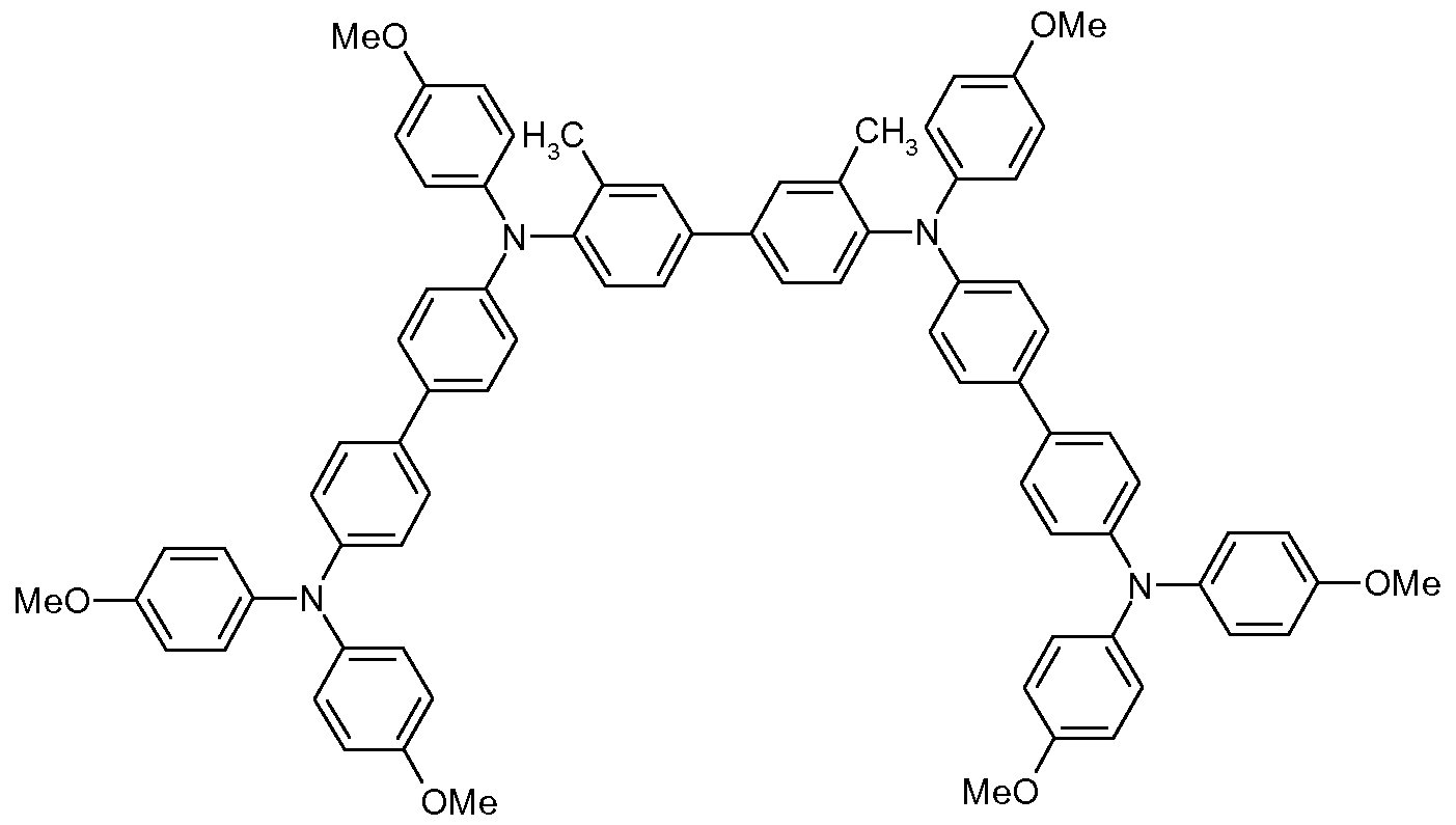
- ACBHJQYJHXYZSY-UHFFFAOYSA-N Cc(cc(cc1)-c(cc2)cc(C)c2N(c(cc2)ccc2-c(cc2)ccc2N(c(cc2)ccc2OC)c(cc2)ccc2OC)c(cc2)ccc2OC)c1N(c(cc1)ccc1-c(cc1)ccc1N(c(cc1)ccc1OC)c(cc1)ccc1OC)c(cc1)ccc1OC Chemical compound Cc(cc(cc1)-c(cc2)cc(C)c2N(c(cc2)ccc2-c(cc2)ccc2N(c(cc2)ccc2OC)c(cc2)ccc2OC)c(cc2)ccc2OC)c1N(c(cc1)ccc1-c(cc1)ccc1N(c(cc1)ccc1OC)c(cc1)ccc1OC)c(cc1)ccc1OC ACBHJQYJHXYZSY-UHFFFAOYSA-N 0.000 description 1
Classifications
-
- C—CHEMISTRY; METALLURGY
- C07—ORGANIC CHEMISTRY
- C07C—ACYCLIC OR CARBOCYCLIC COMPOUNDS
- C07C211/00—Compounds containing amino groups bound to a carbon skeleton
- C07C211/43—Compounds containing amino groups bound to a carbon skeleton having amino groups bound to carbon atoms of six-membered aromatic rings of the carbon skeleton
- C07C211/44—Compounds containing amino groups bound to a carbon skeleton having amino groups bound to carbon atoms of six-membered aromatic rings of the carbon skeleton having amino groups bound to only one six-membered aromatic ring
- C07C211/49—Compounds containing amino groups bound to a carbon skeleton having amino groups bound to carbon atoms of six-membered aromatic rings of the carbon skeleton having amino groups bound to only one six-membered aromatic ring having at least two amino groups bound to the carbon skeleton
- C07C211/50—Compounds containing amino groups bound to a carbon skeleton having amino groups bound to carbon atoms of six-membered aromatic rings of the carbon skeleton having amino groups bound to only one six-membered aromatic ring having at least two amino groups bound to the carbon skeleton with at least two amino groups bound to carbon atoms of six-membered aromatic rings of the carbon skeleton
- C07C211/51—Phenylenediamines
-
- H—ELECTRICITY
- H10—SEMICONDUCTOR DEVICES; ELECTRIC SOLID-STATE DEVICES NOT OTHERWISE PROVIDED FOR
- H10K—ORGANIC ELECTRIC SOLID-STATE DEVICES
- H10K85/00—Organic materials used in the body or electrodes of devices covered by this subclass
- H10K85/60—Organic compounds having low molecular weight
- H10K85/631—Amine compounds having at least two aryl rest on at least one amine-nitrogen atom, e.g. triphenylamine
-
- H—ELECTRICITY
- H10—SEMICONDUCTOR DEVICES; ELECTRIC SOLID-STATE DEVICES NOT OTHERWISE PROVIDED FOR
- H10K—ORGANIC ELECTRIC SOLID-STATE DEVICES
- H10K30/00—Organic devices sensitive to infrared radiation, light, electromagnetic radiation of shorter wavelength or corpuscular radiation
- H10K30/10—Organic devices sensitive to infrared radiation, light, electromagnetic radiation of shorter wavelength or corpuscular radiation comprising heterojunctions between organic semiconductors and inorganic semiconductors
- H10K30/15—Sensitised wide-bandgap semiconductor devices, e.g. dye-sensitised TiO2
- H10K30/151—Sensitised wide-bandgap semiconductor devices, e.g. dye-sensitised TiO2 the wide bandgap semiconductor comprising titanium oxide, e.g. TiO2
-
- H—ELECTRICITY
- H10—SEMICONDUCTOR DEVICES; ELECTRIC SOLID-STATE DEVICES NOT OTHERWISE PROVIDED FOR
- H10K—ORGANIC ELECTRIC SOLID-STATE DEVICES
- H10K85/00—Organic materials used in the body or electrodes of devices covered by this subclass
- H10K85/60—Organic compounds having low molecular weight
- H10K85/631—Amine compounds having at least two aryl rest on at least one amine-nitrogen atom, e.g. triphenylamine
- H10K85/633—Amine compounds having at least two aryl rest on at least one amine-nitrogen atom, e.g. triphenylamine comprising polycyclic condensed aromatic hydrocarbons as substituents on the nitrogen atom
-
- H—ELECTRICITY
- H10—SEMICONDUCTOR DEVICES; ELECTRIC SOLID-STATE DEVICES NOT OTHERWISE PROVIDED FOR
- H10K—ORGANIC ELECTRIC SOLID-STATE DEVICES
- H10K85/00—Organic materials used in the body or electrodes of devices covered by this subclass
- H10K85/60—Organic compounds having low molecular weight
- H10K85/631—Amine compounds having at least two aryl rest on at least one amine-nitrogen atom, e.g. triphenylamine
- H10K85/636—Amine compounds having at least two aryl rest on at least one amine-nitrogen atom, e.g. triphenylamine comprising heteroaromatic hydrocarbons as substituents on the nitrogen atom
-
- H—ELECTRICITY
- H10—SEMICONDUCTOR DEVICES; ELECTRIC SOLID-STATE DEVICES NOT OTHERWISE PROVIDED FOR
- H10K—ORGANIC ELECTRIC SOLID-STATE DEVICES
- H10K85/00—Organic materials used in the body or electrodes of devices covered by this subclass
- H10K85/60—Organic compounds having low molecular weight
- H10K85/649—Aromatic compounds comprising a hetero atom
- H10K85/655—Aromatic compounds comprising a hetero atom comprising only sulfur as heteroatom
-
- C—CHEMISTRY; METALLURGY
- C09—DYES; PAINTS; POLISHES; NATURAL RESINS; ADHESIVES; COMPOSITIONS NOT OTHERWISE PROVIDED FOR; APPLICATIONS OF MATERIALS NOT OTHERWISE PROVIDED FOR
- C09K—MATERIALS FOR MISCELLANEOUS APPLICATIONS, NOT PROVIDED FOR ELSEWHERE
- C09K2211/00—Chemical nature of organic luminescent or tenebrescent compounds
- C09K2211/10—Non-macromolecular compounds
- C09K2211/1003—Carbocyclic compounds
- C09K2211/1011—Condensed systems
-
- H—ELECTRICITY
- H10—SEMICONDUCTOR DEVICES; ELECTRIC SOLID-STATE DEVICES NOT OTHERWISE PROVIDED FOR
- H10K—ORGANIC ELECTRIC SOLID-STATE DEVICES
- H10K30/00—Organic devices sensitive to infrared radiation, light, electromagnetic radiation of shorter wavelength or corpuscular radiation
- H10K30/50—Photovoltaic [PV] devices
-
- Y—GENERAL TAGGING OF NEW TECHNOLOGICAL DEVELOPMENTS; GENERAL TAGGING OF CROSS-SECTIONAL TECHNOLOGIES SPANNING OVER SEVERAL SECTIONS OF THE IPC; TECHNICAL SUBJECTS COVERED BY FORMER USPC CROSS-REFERENCE ART COLLECTIONS [XRACs] AND DIGESTS
- Y02—TECHNOLOGIES OR APPLICATIONS FOR MITIGATION OR ADAPTATION AGAINST CLIMATE CHANGE
- Y02E—REDUCTION OF GREENHOUSE GAS [GHG] EMISSIONS, RELATED TO ENERGY GENERATION, TRANSMISSION OR DISTRIBUTION
- Y02E10/00—Energy generation through renewable energy sources
- Y02E10/50—Photovoltaic [PV] energy
- Y02E10/549—Organic PV cells
Definitions
- triarylamine derivatives as hole-conducting materials in organic solar cells and organic solar cells containing these triarylamine derivatives
- the present invention relates to the use of compounds of general formula I.
- a 1 , A 2 , A 3 are each independently of one another divalent organic units which may contain one, two or three optionally substituted aromatic or heteroaromatic groups, where in the case of two or three aromatic or heteroaromatic groups, two of these groups are each bound by a chemical bond and / or are connected to each other via a divalent alkyl radical,
- R 1 , R 2 , R 3 independently of one another are substituents R, OR, NR 2 , A 3 -OR or A 3 -NR 2 ,
- R is alkyl, aryl or a monovalent organic radical which may contain one, two or three optionally substituted aromatic or heteroaromatic groups, wherein in the case of two or three aromatic or heteroaromatic groups, any two of these groups by a chemical bond and / or via a bivalent Alkyl or NR ' radical are joined together, R 'is alkyl, aryl or a monovalent organic radical which may contain one, two or three optionally substituted aromatic or heteroaromatic groups, wherein in the case of two or three aromatic or heteroaromatic groups, two of these groups by a chemical bond and / or via a divalent alkyl radical are linked together,
- n is independently 0, 1, 2 or 3 for each occurrence in formula I,
- n is at least 2 and at least two of the radicals R 1 , R 2 and R 3 are substituents OR and / or NR 2,
- the present invention relates to organic solar cells containing these compounds.
- Dye solar cells also Dye Solar Cell, “DSC”, or Dye Sensitized Solar Cell, “DSSC”, these terms or abbreviations are used interchangeably below
- DSC Dye Sensitized Solar Cell
- the construction of a DSC is usually based on a glass substrate coated with a transparent, conductive layer, the working electrode.
- an n-type metal oxide is applied, for example, an approximately 10-20 microns thick, nanoporous layer of titanium dioxide (TiO 2).
- TiO 2 titanium dioxide
- the counter electrode may comprise a catalytic layer of a metal, such as platinum, a few microns thick. The area between the two electrodes is covered with a redox electrolyte, z.
- iodine (b) and lithium iodide (LiI) filled.
- the function of the DSC is to absorb light from the dye, transfer electrons from the excited dye to the n-type semiconducting metal oxide semiconductor, and migrate to the anode, whereas the electrolyte ensures charge equalization across the cathode.
- the n-type semiconducting metal oxide, the dye and the (mostly liquid) electrolyte are the essential components of DSC, with cells containing liquid electrolyte in many cases suffering from a non-optimal seal resulting in stability problems. Therefore, various materials have been investigated for their suitability as solid electrolytes / p-type semiconductors.
- various inorganic p-type semiconductors such as CuI, CuBr • 3 (S (C 4 Hg) 2 ) or CuSCN have been used in solid state DSCs.
- efficiencies of up to 3% have been reported with solid DSC based on CuI or CuSCN (Tennakone et al J. Phys D: Appl Phys, 1998, 31, 1492, O'Regan et al., Adv 200, 12, 1263, Kumara et al., Chem. Mater., 2002, 14, 954).
- Organic polymers are also used as solid p-type semiconductors.
- examples thereof include polypyrrole, poly (3,4-ethylenedioxythiophene), carbazole-based polymers, polyaniline, poly (4-undecyl-2,2'-bithiophene), poly (3-octylthiophene), poly (triphenyldiamine), and poly (N vinylcarbazole).
- the efficiencies reach up to 2% in the case of the poly (N-vinylcarbazole), and an efficiency of 2.9% has even been achieved on an in-situ polymerized PEDOT (poly (3,4-ethylenedioxythiophene) (Xia et al. Phys. Chem.
- IPCE incident photon to current conversion efficiency, external photon conversion efficiency
- N (PhBr) sSbCl6 as dopant
- Li [(CF 3 SO 2 ) 2N] an increase in IPCE to 33% and in efficiency to 0.74% was observed.
- tert-butylpyridine the efficiency could be increased to 2.56%, with an open circuit voltage (V oc ) of about 910 mV and a short-circuit current Isc of about 5 mA with an active area of about 1.07 cm 2 (Krüger et al., Appl. Phys.
- solubility in conventional process solvents is relatively low, resulting in a correspondingly low pore filling level.
- the object of the present invention was therefore to provide further compounds which can be used advantageously in solar cells, in particular in DSCs, as p-type semiconductors.
- these compounds should have good hole-conducting properties, have no or only a very slight tendency to crystallize and good in the usual be used solvents to cause the highest possible degree of filling of the oxide pores.
- Alkyl is to be understood as meaning substituted or unsubstituted C 1 -C 20 -alkyl radicals. Preference is given to C 1 -C 10 -alkyl radicals, more preferably C 1 -C -alkyl radicals.
- the alkyl radicals can be both straight-chain and branched.
- the alkyl radicals may be substituted by one or more substituents selected from the group consisting of C 1 -C 20 -alkoxy, halogen, preferably F, and C 6 -C 8 -aryl, which in turn may be substituted or unsubstituted.
- alkyl groups are methyl, ethyl, propyl, butyl, pentyl, hexyl, heptyl and octyl and with C6-C3o-aryl, Ci-C2o-alkoxy and / or halogen, especially F, substituted derivatives of said alkyl groups, for Example CF3.
- linear and branched alkyl radicals are methyl, ethyl, propyl, butyl, pentyl, hexyl, heptyl and octyl and isopropyl, isobutyl, isopentyl, sec-butyl, tert-butyl, neopentyl, 3,3-dimethylbutyl, 2-ethylhexyl ,
- Divalent alkyl radicals in the units A 1 , A 2 , A 3 , R, R ' , R 4 , R 5 , R 6 , R 7 , R 8 and R 9 are derived from the aforementioned alkyl by formal removal of another From the hydrogen atom.
- Suitable aryls are C ⁇ -Cso-aryl radicals derived from monocyclic, bicyclic or tricyclic aromatics which contain no ring heteroatoms. Unless they are monocyclic systems, the term aryl for the second ring also means the saturated form (perhydroform) or the partially unsaturated form (for example the dihydroform or tetrahyroform), provided the respective forms are known and stable. Thus, for the purposes of the present invention, the term aryl also includes, for example, bicyclic or tricyclic radicals in which both both and all three radicals are aromatic, as well as bicyclic or tricyclic radicals in which only one ring is aromatic, and tricyclic radicals in which two Rings are aromatic.
- aryl examples include: phenyl, naphthyl, indanyl, 1, 2-dihydronaphthenyl, 1, 4-dihydronaphthenyl, fluorenyl, indenyl, anthracenyl, phenanthrenyl or 1, 2,3,4-tetrahydronaphthyl.
- Particularly preferred are C ⁇ -Cio-aryl radicals, for example phenyl or naphthyl, very particularly preferably C ⁇ -aryl radicals, for example phenyl.
- Aromatic groups in the units A 1 , A 2 , A 3 , R, R ' , R 4 , R 5 , R 6 , R 7 , R 8 and R 9 are derived from the aforementioned aryl by formal removal of one or more others Hydrogen atoms off.
- Heteroaromatic groups in the units A 1 , A 2 , A 3 , R, R ' , R 4 , R 5 , R 6 , R 7 , R 8 and R 9 are derived from hetaryl radicals by formal removal of one or more others Hydrogen atoms off.
- hetaryl radicals are unsubstituted or substituted here and contain 5 to 30 ring atoms. They may be monocyclic, bicyclic or tricyclic and may be derived, in part, from the abovementioned aryl, in which at least one carbon atom in the aryl skeleton is replaced by a heteroatom. Preferred heteroatoms are N, O and S. Particularly preferably, the
- the backbone of the heteroaryl radicals selected from systems such as pyridine and five-membered heteroaromatics such as thiophene, pyrrole, imidazole or furan. These backbones may optionally be fused with one or two six-membered aromatic radicals. Suitable fused heteroaromatics are carbazolyl, benzimidazolyl, benzofuryl, dibenzofuryl or dibenzothiophenyl.
- the backbone may be substituted at one, several or all substitutable positions, suitable substituents being the same as those already mentioned under the definition of C ⁇ -Cso-aryl.
- hetaryl radicals are preferably unsubstituted.
- Suitable hetaryl radicals are, for example, pyridin-2-yl, pyridin-3-yl, pyridin-4-yl, thiophen-2-yl, thiophen-3-yl, pyrrol-2-yl, pyrrol-3-yl, furan-2 -yl, furan-3-yl and imidazol-2-yl and the corresponding benzanell faced radicals, in particular carbazolyl, benzimidazolyl, benzofuryl, dibenzofuryl or dibenzothiophenyl.
- substituents of the one, two or three optionally substituted aromatic or heteroaromatic groups are alkyl radicals, such as methyl, ethyl, propyl, butyl, pentyl, hexyl, heptyl and octyl and isopropyl, isobutyl, isopentyl, sec-butyl, tert Butyl, neopentyl, 3,3-dimethylbutyl and 2-ethylhexyl, aryl radicals, such as C ⁇ -C-io-Arvl radicals, in particular phenyl or naphthyl, most preferably C ⁇ -aryl radicals, for example phenyl, and hetaryl Radicals, such as, for example, pyridin-2-yl, pyridin-3-yl, pyridin-4-yl, thiophen-2-yl, thiophen-3-yl, pyrrol-2-yl,
- Preferred compounds of the formula I to be used according to the invention are characterized in that at least two of the radicals R 1 , R 2 and R 3 are para-substituted OR and / or NR 2 substituents. Hiebei there may be at least two residues either only OR residues, only NR2 residues or at least one OR and act at least one NF ⁇ -Rest.
- Particularly preferred compounds of the formula I to be used according to the invention are characterized in that at least four of the radicals R 1 , R 2 and R 3 are para-containing OR and / or NR 2 substituents. Hiebei may be at least four residues either only OR residues, only NR2 residues or a mixture of OR and NR2 residues.
- Very particularly preferred compounds of the formula I to be used according to the invention are distinguished by the fact that all radicals R 1 , R 2 and R 3 are para-substituted OR and / or NR 2 substituents. These can be either only OR residues, only NR2 residues, or a mixture of OR and NR2 residues.
- the two Rs in the NR2 residues may be different from each other, but they are preferably the same.
- Preferred bivalent organic units A 1 , A 2 and A 3 are selected from the group consisting of (CH 2 ) m , C (R 7 ) (R 8 ), N (R 9 ),
- n is an integer value from 1 to 18,
- R 4 , R 9 is alkyl, aryl or a monovalent organic radical which may contain one, two or three unsubstituted or substituted aromatic or heteroaromatic groups, where in the case of two or three aromatic or heteroaromatic groups, two of these groups are each bound by a chemical bond and / or are connected to each other via a divalent alkyl radical, R 5 , R 6 , R 7 , R 8 independently of one another are hydrogen atoms or radicals of the definition of R 4 and R 9 ,
- the degree of substitution of the aromatic and heteroaromatic rings can vary from simple substitution to the maximum number of possible substituents.
- Preferred substituents in the case of a further substitution of the aromatic and heteroaromatic rings are the substituents already mentioned above for the one, two or three optionally substituted aromatic or heteroaromatic groups.
- the compounds to be used according to the invention can be prepared by customary methods of organic synthesis known to those skilled in the art. References to relevant (patent) references can also be found in the Synthesis Examples below.
- n-semiconducting metal oxide For the construction of a DSC, a single metal oxide or a mixture of different oxides can be used as the n-semiconducting metal oxide. It is also possible to use mixed oxides.
- the n-semiconducting metal oxide can be used in particular as a nanoparticulate oxide, in which context nanoparticles are to be understood as meaning particles having an average particle size of less than 0.1 micrometers.
- a nanoparticulate oxide is usually applied to a conductive substrate (i.e., a substrate having a conductive layer as a first electrode) by a sintering process as a thin porous film having a large surface area.
- a substrate As a substrate (hereinafter also referred to as a support) are in addition to metal foils especially plastic sheets or films and glass plates in particular.
- electrode material in particular for the first electrode according to the preferred structure described above, in particular conductive materials such.
- transparent conductive oxides transparent conducting oxides, TCO
- FTO or ITO fluorine and / or indium-doped tin oxide
- AZO aluminum-doped zinc oxide
- carbon nanotubes or metal films Alternatively or additionally, however, it would also be possible to use thin metal films which still have sufficient transparency.
- the substrate may be coated with these conductive materials. Since in this structure usually only a single substrate is needed, the construction of flexible cells is possible. This allows a variety of applications that would not or only with realizable rigid substrates, such as the use in bank cards, garments, etc.
- the first electrode in particular the TCO layer, can additionally be coated or coated with a (for example 10 to 200 nm thick) solid buffer layer, in particular a metal oxide buffer layer, in order to direct contact of the p-type semiconductor with the TCO layer (see Peng et al., Coord. Chem. Rev. 248, 1479 (2004)).
- the buffer metal oxide which may be employed in the buffer layer may comprise, for example, one or more of the following materials: vanadium oxide; a zinc oxide; a tin oxide; a titanium oxide.
- Thin layers or films of metal oxides are usually inexpensive solid semiconductor materials (n-type semiconductors), but their absorption is due to large band gaps usually not in the visible range of the solar spectrum, but predominantly in the ultraviolet spectral range.
- the metal oxides must generally, as is the case with the DSCs, be combined with a dye as a photosensitizer, which absorbs in the wavelength range of sunlight, ie at 300 to 2000 nm, and electrons in the electronically excited state injected into the conduction band of the semiconductor.
- a dye as a photosensitizer
- nanorods nanorods
- advantages such as higher electron mobilities or improved pore filling by the dye and the p-type semiconductor.
- the metal oxide semiconductors can be used alone or in the form of mixtures. It is also possible to coat a metal oxide with one or more other metal oxides. Furthermore, the metal oxides may also be used as a coating on another semiconductor, e.g. As GaP, ZnP or ZnS, be applied.
- Particularly preferred semiconductors are zinc oxide and titanium dioxide in the anatase modification, which is preferably used in nanocrystalline form.
- the sensitizers can be advantageously combined with all the n-type semiconductors commonly used in these solar cells.
- Preferred examples are metal oxides used in the ceramic, such as titanium dioxide, zinc oxide, tin (IV) oxide, tungsten (VI) oxide, tantalum (V) oxide, niobium (V) oxide, cesium oxide, strontium titanate, zinc stannate, complex oxides of the perovskite type, e.g. As barium titanate, and called binary and ternary iron oxides, which may also be present in nanocrystalline or amorphous form.
- n-semiconducting metal oxide Due to the strong absorption exhibited by common organic dyes as well as phthalocyanines and porphyrins, even thin layers or films of the dye-sensitized n-type semiconductive metal oxide are sufficient to obtain sufficient light absorption. Thin metal oxide films in turn have the advantage that the probability of undesired recombination processes decreases and that the internal resistance of the dye subcell is reduced. Layer thicknesses of from 100 nm to 20 micrometers can preferably be used for the n-semiconducting metal oxide, more preferably in the range between 500 nm to about 5 micrometers.
- dye-sensitized solar cells based on titanium dioxide as a semiconductor material are, for. In US-A-4,927,721, Nature 353, pp. 737-740 (1991) and US-A-5,350,644 and Nature 395, pp. 583-585 (1998) and EP-A-1 176 646 described.
- the dyes described in these documents can in principle also be used advantageously in the context of the present invention.
- These dye-sensitized solar cells contain monomolecular films of transition metal complexes, in particular ruthenium complexes, which are bonded to the titanium dioxide layer via acid groups as sensitizers.
- Sensitizers not least for reasons of cost, have repeatedly been proposed metal-free organic dyes which can also be used in the context of the present invention.
- Indoline dyes achieve (see, for example, Schmidt-Mende et al., Adv., Mater., 2005, 17, 813).
- US Pat. No. 6,359,211 also describes the use, within the scope of the present invention, of cyanine, oxazine, thiazine and acridine dyes which have carboxyl groups bonded via an alkylene radical for attachment to the titanium dioxide semiconductor.
- JP-A-10-189065, 2000-243463, 2001-093589, 2000-100484 and 10-334954 describe various perylene skeleton unsubstituted perylene-3,4: 9,10-tetracarboxylic acid derivatives for use in semiconductor solar cells.
- perylenetetracarboxylic diimides which carry carboxyalkyl, carboxyaryl, carboxyarylalkyl or carboxyalkylaryl radicals on the imide nitrogen atoms and / or are imidated with p-diaminobenzene derivatives in which the nitrogen atom of the amino group is substituted by two further phenyl radicals in the p-position Part of a heteroaromatic tricyclic system;
- Perylene-3,4 9,10-tetracarboxylic monoanhydride monoimides bearing on the imide nitrogen atom the radicals mentioned above or non-functionalized alkyl or aryl radicals, or
- Sensibilisatorfabstoffe in the proposed dye solar cell are described in DE 10 2005 053 995 A1 or WO 2007/054470 A1 perylene derivatives, Terrylenderivate and Quaterrylenderivate.
- the use of these dyes leads to photovoltaic elements with high efficiencies and high stabilities.
- the rylenes show strong absorption in the wavelength range of the sunlight and can, depending on the length of the conjugated system, a range of about 400 nm (perylene derivatives I from DE 10 2005 053 995 A1) up to about 900 nm (quaterrylene derivatives I from DE 10 2005 053 995 A1).
- terrylene-based rylene derivatives I absorb in a solid state adsorbed to titanium dioxide in a range from about 400 to 800 nm.
- the rylene derivatives I can be easily and permanently fixed on the metal oxide film. Binding takes place via the anhydride function (x1) or the carboxyl groups -COOH or -COO- formed in situ or via the acid groups A contained in the imide or condensate radicals ((x2) or (x3)) Rylene derivatives I described in DE 10 2005 053 995 A1 are well suited for use in dye-sensitized solar cells in the context of the present invention.
- the dyes have an anchor group at one end of the molecule, which ensures their fixation on the n-type semiconductor film.
- the dyes preferably contain electron donors which facilitate regeneration of the dye after electron donation to the n-type semiconductor and also prevent recombination with electrons already delivered to the semiconductor.
- the fixation of the dyes on the metal oxide films can be done in a simple manner.
- the n-type semiconductive metal oxide films in freshly sintered (still warm) condition may be contacted with a solution or suspension of the dye in a suitable organic solvent for a sufficient period of time (eg, about 0.5 to 24 hours). This can be done, for example, by immersing the substrate coated with the metal oxide in the solution of the dye.
- combinations of different dyes are to be used, they can be applied, for example, one after the other from one or more solutions or suspensions containing one or more of the dyes. Also possible is the use of two dyes separated by a layer of z. CuSCN (see eg Tennakone, K.J., Phys. Chem B. 2003, 107, 13758). The most appropriate method can be determined comparatively easily in individual cases.
- the dye can be present as a separate element or applied in a separate step and applied separately to the remaining layers.
- the dye can also be combined with one or more of the other elements or applied together, for example with the solid p-type semiconductor. So can for example, a dye-p-semiconductor combination comprising an absorbent dye having p-type semiconductive properties or, for example, a pigment having absorbent and p-type semiconductive properties can be used.
- a kind of passivating layer comprising a passivation material.
- This layer should be as thin as possible and, if possible, should only cover the hitherto uncovered areas of the n-semiconducting metal oxide.
- the passivation material may also be applied to the metal oxide in time before the dye.
- passivation materials in particular the following substances are preferred: Al 2 O 3; an aluminum salt; Silanes, such as For example, CHsSiCb; an organometallic complex, in particular an Al 3+ complex; Al 3+ , in particular an Al 3+ complex; 4-tert-butyl pyridine in (TBP); MgO; 4-guanidinobutyric acid (GBA); an alkanoic acid; Hexadecylmalonic acid (HDMA).
- Silanes such as For example, CHsSiCb
- an organometallic complex in particular an Al 3+ complex
- Al 3+ in particular an Al 3+ complex
- MgO 4-guanidinobutyric acid
- GAA 4-guanidinobutyric acid
- HDMA Hexadecylmalonic acid
- solid p-type semiconductors are used in the solid-colorant solar cell.
- Solid p-type semiconductors can also be used in the dye-sensitized soot cells according to the invention without a large increase in cell resistance, in particular if the dyes absorb strongly and therefore require only thin n-type semiconductor layers.
- the p-type semiconductor should essentially have a closed, dense layer in order to reduce unwanted recombination reactions which could result from contact between the n-semiconducting metal oxide (in particular in nanoporous form) with the second electrode or the second half cell.
- the compounds of the formula I can be prepared via the sequence of the synthesis steps of the synthesis route I shown above.
- the coupling of the reactants can be carried out, for example, by Ullmann reaction with copper as catalyst or under palladium catalysis.
- the compounds of the formula I can be prepared via the sequence of the synthesis steps of the synthesis route II shown above.
- the coupling of the reactants can, as in Synthesis Route I, for example, by Ullmann reaction with copper as catalyst or under palladium catalysis. Production of the starting amines:
- diarylamines are not commercially available in the synthesis steps I-R2 and II-R1 of the synthesis routes I and II, they can be prepared, for example, by Ullmann reaction with copper as catalyst or under palladium catalysis in accordance with the following reaction:
- reaction mixture was heated for 7 hours at a temperature of 100 0 C under a nitrogen atmosphere. After cooling to room temperature, the reaction mixture was quenched with ice-water, the precipitate filtered off and dissolved in ethyl acetate. The organic layer was washed with water, dried over sodium sulfate and purified by column chromatography (eluent: 5% ethyl acetate / hexane). A slightly yellow colored solid was obtained (7.58 g, yield: 82%).
- N 4 , N 4 '-Bis (4-methoxyphenyl) biphenyl-4,4'-diamine product from Synthesis Step I-R1, 0.4 g, 1.0 mmol
- product from Synthesis Step I-R2 (1, 0 2.2 mmol) were added under a nitrogen atmosphere to a solution of t-BuONa (0.32 g, 3.3 mmol) in o-xylene (25 mL).
- palladium acetate (0.03 g, 0.14 mmol
- 10 wt% P (t-Bu) 3 tris-t-butylphosphine
- reaction mixture was diluted with 150 ml of toluene, filtered through Celite® and the organic layer was dried over Na 2 SO 4. The solvent was removed and the crude product was reprecipitated three times from a mixture of tetrahydrofuran (THF) / methanol.
- THF tetrahydrofuran
- the solid was purified by column chromatography (eluent: 20% ethyl acetate / hexane) followed by precipitation with THF / methanol and charcoal purification. After removal of the solvent, the product was obtained as a pale yellow solid (1, 0g, yield: 86%).
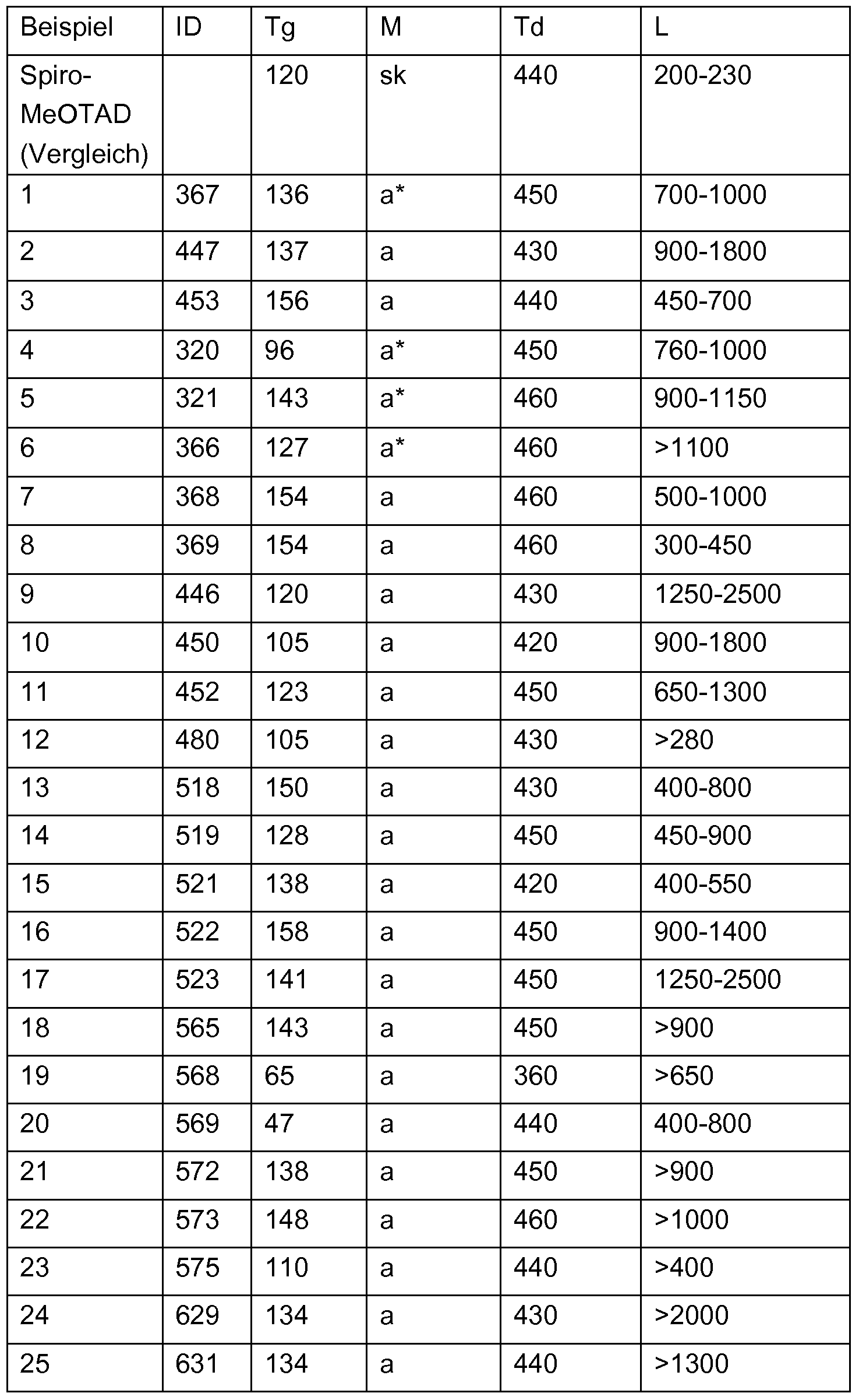
- Table 1 shows that the compounds to be used according to the invention are consistently present in amorphous form. Therefore, they are expected to have a significantly lower tendency for crystallization and to provide more advantageous properties of the DSCs produced therewith in terms of extended life than DSCs based on the comparative compound spiro-MeOTAD. Furthermore the compounds to be used according to the invention have a significantly better solubility than the comparative compound spiro-MeOTAD, which has a positive effect on the pore filling level in the preparation of the DSCs.
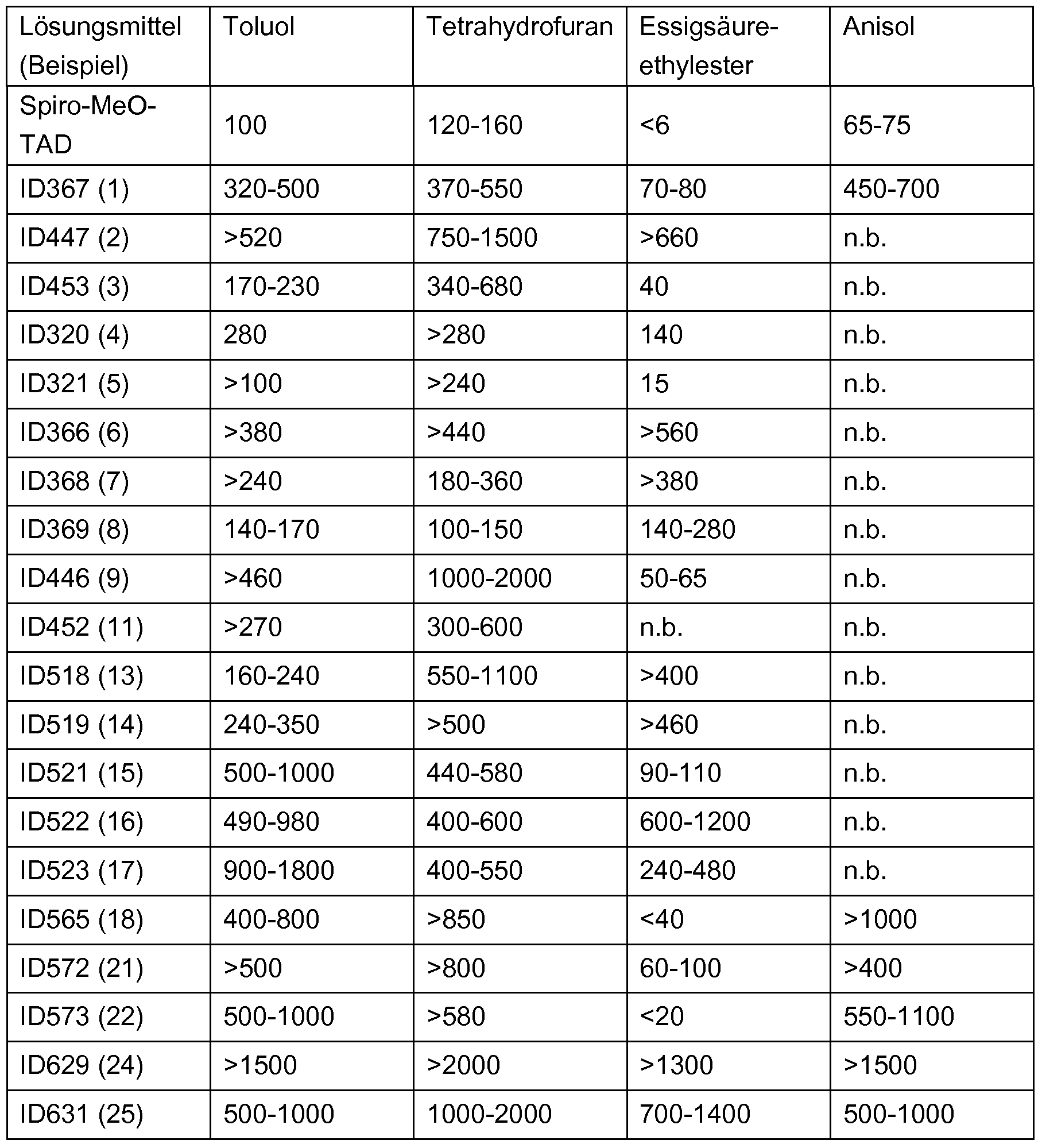
- chlorobenzene has low to moderate toxicity (LD50 of 2.9 g / kg according to Manfred Rossberg et al., "Chlorinated Hydrocarbons” in Ullmann's Encyclopedia of Industrial Chemistry Wiley-VCH, Weinheim, 2006), the compounds were also exemplified by their solubility in investigated other solvents. How one
- TCO - transparent conducting oxide such as FTO (fluorine-doped tin oxide) or ITO (indium tin oxide).
- FTO fluorine-doped tin oxide
- ITO indium tin oxide
- an optional buffer layer 119 can be applied, which should prevent or at least complicate the migration of the holes to the front electrode 116.
- the buffer layer 119 used is usually a single layer of (preferably non-nanoporous) titanium dioxide and generally has a thickness between 10 nm and 500 nm. Such layers can be produced, for example, by sputtering and / or spray pyrolysis.
- the optional buffer layer 119 is followed by an approximately 1 ⁇ m to 20 ⁇ m thick layer 120 of a porous, n-semiconductive metal oxide, which is sensitized with a very thin, usually monomolecular layer 122 of a dye.
- n-type semiconducting metal oxide titanium dioxide, but other oxides are conceivable.
- the layer 120 of the n-type semiconducting metal oxide sensitized with the dye (layer 122) is followed by a layer 123 of hole-conducting material.
- This material fills the pores of the layer 120/122 (metal oxide / dye) usually more or less completely, with a possible complete degree of filling is desirable. This results in an interpenetrating layer / intimate penetration of hole-conducting material and n-type semiconducting metal oxide / dye.
- the hole-conducting material on the metal oxide / dye layer forms a supernatant layer 124, which is typically 10 nm to 500 nm thick and, inter alia, prevents electrons from the metal oxide from entering the cathode 138.
- a counter electrode 138 is applied as a top contact (cathode).
- front contact (anode) 1 16 and the top contact (cathode) 138 are provided with corresponding conductive terminals, but not shown here for reasons of clarity were.
- Example I24 24 on page 109 of WO 2007/054470 A1 was reacted with 8 equivalents of glycine and one equivalent of anhydrous zinc acetate in N-methylpyrrolidone at 130 0 C overnight.
- the product was purified over silica gel.
- the test DSCs were prepared as follows:
- the base material used was nippon sheet glass 25 mm x 15 mm x 3 mm glass plates coated with fluorine-doped tin oxide (FTO), which were treated successively with glass cleaner (RBS 35), demineralized water and acetone for 5 minutes each in an ultrasonic bath, then Boiled for 10 minutes in isopropanol and dried in a stream of nitrogen.
- FTO fluorine-doped tin oxide
- a layer of an n-type semiconducting metal oxide 120 was applied on the buffer layer 1 19, a layer of an n-type semiconducting metal oxide 120 was applied.
- a Ti ⁇ 2 paste (Dyesol, DSL 18NR-T), spin coated with a spin coater at 4500 revolutions per minute and dried at 90 0 C for 30 minutes. After 45 minutes of heating to 450 0 C and 30-minute sintering at 450 0 C, a TiO 2 layer thickness resulted from approximately 1, 8 microns.
- the sample After removal from the sintering furnace, the sample was cooled to 80 0 C and immersed for 12 hours in a 0.5 mM solution of the dye D102 in acetonitrile / t-BuOH 1: 1. After removal from the solution, the sample was then rinsed with the same solvent and dried in a stream of nitrogen.
- the p-type semiconductor ID367 was deposited. To this was added a solution of 130 mM ID367, 12 mM LiN (SO 2 CFs) 2 (Aldrich), 47 mM 4-t-butylpyridine (Aldrich) in chlorobenzene. 75 ⁇ l of this solution was applied to the sample and allowed to act for 60 seconds. Thereafter, the supernatant solution was spun for 30 seconds at 2000 revolutions per minute and dried in ambient air for 3 hours.
- the top contact (cathode) was applied by thermal metal evaporation in vacuo.
- the sample was provided with a mask to vaporize 4 individual, separate rectangular top contacts with dimensions of about 5 mm x 4 mm on the active region, each with an approximately 3 mm x 2 mm contact surface are connected.
- the metal Ag came to be used, the s 5 mbar was evaporated at a pressure of 5 ⁇ 10 "at a rate of 0.1 nm /, so that a layer of about 200 nm thickness was formed.
- the respective current / voltage characteristic was measured with a Source Meter Model 2400 (Keithley Instruments Inc.) under irradiation with a xenon lamp (LOT-Oriel) as a solar simulator.
- the short-circuit current density Isc (SC stands for "short circuit") was 1.01 mA / cm 2 or 9.76 mA / cm 2 , the terminal voltage Voc (OC stands in this case for "open circuit”) with open circuit 0.78 V or 0.86 V, the fill factor (FF) 68% or 53% and the efficiency 5.3% and 4.4%, respectively.
- Comparative Example to DSC 1 As described in example DSC 1, a solid DSC was produced with the hole conductor spiro-MeO-TAD. To this was added a solution of 163 mM spiro-MeO-TAD, 15 mM LiN (SO 2 CFs) 2 (Aldrich), 60 mM 4-t-butylpyridine (Aldrich) in chlorobenzene.
- the short-circuit current density Isc (SC stands for “short circuit”) was 1.10 mA / cm 2 or 10.60 mA / cm 2 , the terminal voltage Voc (OC stands here for “open circuit”) with open circuit 0.74 V or 0.80 V, the fill factor (FF) 69% or 47% and the efficiency 5.6% and 4.0%.
- a solid DSC was prepared with the hole conductor ID447 and the dye D102 (hole conductor solution: 167 mM ID447, 15 mM LiN (SO 2 CF 3 ) 2 , 61 mM 4-t-butylpyridine in chlorobenzene).
- the short-circuit current density Isc was 0.91 mA / cm 2 and 6.95 mA / cm 2 , respectively, and the terminal voltage Voc when the circuit was open was 0.72 V and 0.78 V, respectively , the fill factor (FF) 56% and 33% and the efficiency 3.8% and 1, 8%, respectively.
- a solid DSC was prepared with the hole conductor ID453 and the dye D102 (hole conductor solution: 151 mM ID453, 14 mM LiN (SO 2 CF 3 ) 2 , 55 mM 4-t-butylpyridine in chlorobenzene).
- the short-circuit current density Isc was 0.87 mA / cm 2 and 7.75 mA / cm 2 , respectively, and the terminal voltage Voc with the open circuit was 0.84 V and 0.90 V, respectively , the fill factor (FF) 61% and 34% and the efficiency 4.5% and 2.3%.
- a solid DSC was prepared with the hole conductor ID522 and the dye D102 (hole conductor solution: 161 mM ID522, 15 mM LiN (SO 2 CF 3) 2, 58 mM 4-t-butylpyridine in chlorobenzene).
- the thickness of the nanoporous Ti ⁇ 2 layer was this time about 2.2 microns instead of about 1, 8 microns.
- the short-circuit current density Isc was 0.83 mA / cm 2 and 8.77 mA / cm 2 , respectively, and the terminal voltage Voc with the circuit open was 0.76 V and 0.84 V, respectively , the fill factor (FF) 69% and 45% and the efficiency 4.4% and 3.3%, respectively.
- a solid DSC was prepared with the hole conductor spiro-MeO-TAD and the dye D102 (hole-conductor solution: 163 mM spiro-MeO-TAD, 15 mM LiN (SO 2 CFs) 2 (Aldrich), 60 mM 4-t-butylpyridine (Aldrich) in chlorobenzene).
- the thickness of the nanoporous TiO 2 layer was about 2.2 ⁇ m, as in example DSC 4.
- the short-circuit current density Isc was 0.92 mA / cm 2 and 9.10 mA / cm 2 , respectively, and the terminal voltage Voc when the circuit was open was 0.74 V and 0.82 V, respectively , the fill factor (FF) 69% and 50% and the efficiency 4.7% and 3.7%, respectively.
- a solid DSC was prepared with hole-punch ID572 and dye D102 (hole-transfer solution: 178 mM ID572, 16 mM LiN (SO 2 CFs) 2 , 65 mM 4-t-butylpyridine in chlorobenzene).
- the thickness of the nanoporous TiO 2 layer was about 1, 8 microns as in Example DSC 1.
- the short-circuit current density Isc was 0.91 mA / cm 2 and 8.52 mA / cm 2, the terminal voltage Voc open circuit 0.84 V and 0.92 V , the fill factor (FF) 58% and 40% and the efficiency 4.5% and 3.1%, respectively.
- Example DSC 1 a solid DSC was prepared with the hole conductor ID367 and the dye D205 (hole conductor solution: 130 mM ID367, 12 mM LiN (SO 2 CFs) 2 , 47 mM 4-t-butylpyridine in chlorobenzene).
- the short-circuit current density Isc was 0.97 mA / cm 2 and 8.92 mA / cm 2 , respectively, and the terminal voltage Voc when the circuit was open was 0.80 V and 0.88 V, respectively , the fill factor (FF) 70% and 46% and the efficiency 5.4% and 3.7%, respectively.
- a solid DSC was prepared with the hole conductor spiro-MeO-TAD and the dye D205 (hole conductor solution: 123 mM spiro-MeO-TAD, 1 1 mM LiN (SO 2 CFs) 2 , 45 mM 4. t-butylpyridine in chlorobenzene).
- the short-circuit current density Isc was 0.96 mA / cm 2 or
- DSC 7 As described in example DSC 6, a solid DSC was prepared with the hole conductor ID518 and the dye D205 (hole conductor solution: 202 mM ID518, 18 mM LiN (SO 2 CFs) 2 , 74 mM 4-t-butylpyridine in chlorobenzene ). The thickness of the nanoporous TiO 2 layer was this time 3.2 microns instead of about 1, 8 microns.
- the short-circuit current density Isc was 0.81 mA / cm 2 or
- Comparative Example to DSC 7 As described in example DSC 7, a solid DSC was prepared with the hole conductor spiro-MeO-TAD and the dye D205 (hole conductor solution: 204 mM spiro-MeO-TAD, 19 mM LiN (SO 2 CF 3 ). 2, 74 mM 4-t-butylpyridine in chlorobenzene). The thickness of the nanoporous TiO 2 layer was 3.2 ⁇ m, as in DSC 7, instead of approximately 1.8 ⁇ m.
- the short-circuit current density Isc was 0.95 mA / cm 2 or
- DSC 8 As described in example DSC 7, a solid DSC was prepared with the hole conductor ID522 and the dye D205 (hole conductor solution: 201 mM ID522, 18 mM LiN (SO 2 CFs) 2 , 73 mM 4-t-butylpyridine in chlorobenzene) , The thickness of the nanoporous TiO 2 layer was 3.2 ⁇ m, as in DSC 7, instead of approximately 1.8 ⁇ m.
- the short-circuit current density Isc was 0.56 mA / cm 2 or
- a solid DSC was prepared with the hole conductor ID523 and the dye D205 (hole conductor solution: 214 mM ID523, 19 mM LiN (SO 2 CF 3) 2, 78 mM 4-t-butylpyridine in chlorobenzene).
- the thickness of the nanoporous TiO 2 layer was as in DSC 7 3.2 microns instead of about 1, 8 microns.
- the short-circuit current density Isc was 0.95 mA / cm 2 and 6.76 mA / cm 2 , respectively, and the terminal voltage Voc when the circuit was open was 0.74 V and 0.80 V, respectively , the fill factor (FF) 58% and 34% and the efficiency 4.1% and 1, 8%.
- Example DSC 1 a solid DSC was prepared with the hole conductor ID367 and the dye Peryleni (dye bath: 0.5 mM solution of the dye Peryleni in dichloromethane). To this was added a solution of 130 mM ID367, 12 mM LiN (SO 2 CF 3 ) 2 (Aldrich), 47 mM 4-t-butylpyridine (Aldrich) in chlorobenzene.
- the short-circuit current density Isc (SC stands for “short circuit”) was 0.38 mA / cm 2 or 2.78 mA / cm 2 , the terminal voltage Voc (OC stands in this case for "open circuit”) with open circuit 0.66 V or 0.74 V, the fill factor (FF) 53% or 51% and the efficiency 1, 3% or 1, 1%.
- a solid DSC was prepared with the hole conductor spiro-MeO-TAD and the dye Peryleni (dye bath: 0.5 mM solution of the dye Peryleni in dichloromethane). To this was added a solution of 123 mM spiro-MeO-TAD, 1 lmM LiN (SO 2 CFs) 2 (Aldrich), 45 mM 4-t-butylpyridine (Aldrich) in chlorobenzene.
- the short-circuit current density Isc (SC stands for “short circuit”) was 0.37 mA / cm 2 or 2.58 mA / cm 2 , the terminal voltage Voc (OC stands here for “open circuit”) with open circuit 0.60 V or 0.68 V, the fill factor (FF) 55% or 54% and the efficiency 1, 2% and 0.9%.
- Example DSC 1 a solid DSC was prepared with the hole conductor ID367 and the dye perylene 2 (dye bath: 0.5 mM solution of the dye perylene 2 in dichloromethane). To this was added a solution of 130 mM ID367, 12 mM LiN (SO 2 CFs) 2 (Aldrich), 47 mM 4-t-butylpyridine (Aldrich) in chlorobenzene.
- the short-circuit current density Isc (SC stands for “short circuit") was 0.42 mA / cm 2 or 4.39 mA / cm 2 , the terminal voltage Voc (OC stands in this case for "open circuit”) with open circuit 0.78 V or 0.84 V, the fill factor (FF) 68% or 54% and the efficiency 2.3% or 2.0%.
- Comparative Example DSC 11 As described in example DSC 10, a solid DSC was prepared with the hole conductor spiro-MeO-TAD and the dye perylene 2 (dye bath: 0.5 mM solution of the dye perylene 2 in dichloromethane). To this was added a solution of 123 mM spiro-MeO-TAD, 1 lmM LiN (SO 2 CFs) 2 (Aldrich), 45 mM 4-t-butylpyridine (Aldrich) in chlorobenzene.
- the short-circuit current density Isc (SC stands for “short circuit”) was 0.52 mA / cm 2 or 6.87 mA / cm 2
- the terminal voltage Voc (OC stands in this case for "open circuit") with open circuit 0.74 V or 0.76 V
- the fill factor (FF) 70% or 56% and the efficiency 2.7% and 2.9%.
- a solid DSC was prepared with the hole conductor ID523 and the dye perylene 3 (dye bath: 0.5 mM solution of the dye perylene 3 in dichloromethane). To this was added a solution of 214 mM ID523, 19 mM LiN (SO 2 CF 2 ) 2 (Aldrich), 78 mM 4-t-butylpyridine (Aldrich) in chlorobenzene.
- the thickness of the nanoporous TiO 2 layer was about 3.1 microns instead of about 1, 8 microns.
- the short-circuit current density Isc (SC stands for “short circuit”) was 0.21 mA / cm 2 or 3.40 mA / cm 2 , the terminal voltage Voc (OC stands in this case for "open circuit”) with open circuit 0.64 V or 0.66 V, the fill factor (FF) 64% or 59% and the efficiency 0.9% or 1.3%.
- a solid DSC was prepared with the hole conductor spiro-MeO-TAD and the dye perylene 3 (dye bath: 0.5 mM solution of the dye perylene 3 in dichloromethane). To this was added a solution of 204 mM spiro-MeO-TAD, 19 mM LiN (SO 2 CF 2 ) 2 (Aldrich), 74 mM 4-t-butylpyridine (Aldrich) in chlorobenzene. The thickness of the nanoporous TiO 2 layer was about 3.1 microns instead of about 1, 8 microns.
- the short-circuit current density Isc (SC stands for “short circuit”) was 0.25 mA / cm 2 or 3.97 mA / cm 2 , the terminal voltage Voc (OC stands here for “open circuit”) with open circuit 0.62 V or 0.66 V, the fill factor (FF) 66% or 57% and the efficiency 1, 0% and 1, 5%.
Landscapes
- Chemical & Material Sciences (AREA)
- Physics & Mathematics (AREA)
- Spectroscopy & Molecular Physics (AREA)
- Engineering & Computer Science (AREA)
- Materials Engineering (AREA)
- Inorganic Chemistry (AREA)
- Electromagnetism (AREA)
- Organic Chemistry (AREA)
- Photovoltaic Devices (AREA)
- Hybrid Cells (AREA)
- Organic Low-Molecular-Weight Compounds And Preparation Thereof (AREA)
Abstract
Description




Claims



Priority Applications (7)
| Application Number | Priority Date | Filing Date | Title |
|---|---|---|---|
| CN2010800086163A CN102326271A (zh) | 2009-02-23 | 2010-02-15 | 三芳基胺衍生物在有机太阳能电池中作为空穴传导材料的用途和含有所述三芳基衍生物的有机太阳能电池 |
| JP2011550532A JP5698155B2 (ja) | 2009-02-23 | 2010-02-15 | 有機太陽電池における正孔輸送材料としてのトリアリールアミン誘導体の使用、及び前記トリアリールアミン誘導体を含む有機太陽電池 |
| US13/202,878 US20110297235A1 (en) | 2009-02-23 | 2010-02-15 | Use of triarylamine derivatives as hole-conducting materials in organic solar cells and organic solar cells containing said triarylamine derivatives |
| AU2010215568A AU2010215568B2 (en) | 2009-02-23 | 2010-02-15 | Use of triarylamine derivatives as hole-conducting materials in organic solar cells and organic solar cells containing said triarylamine derivatives |
| EP10704140A EP2399305A1 (de) | 2009-02-23 | 2010-02-15 | Verwendung von triarylamin-derivaten als lochleitende materialien in organischen solarzellen und diese triarylamin-derivate enthaltende organische solarzellen |
| ZA2011/06889A ZA201106889B (en) | 2009-02-23 | 2011-09-21 | Use of triarylamine derivatives as hole-conducting materials in organic solar cells and organic solar cells containing said triarylamine derivatives |
| US14/063,723 US20140130870A1 (en) | 2009-02-23 | 2013-10-25 | Use of triarylamine derivatives as hole-conducting materials in organic solar cells and organic solar cells containing said triarylamine derivatives |
Applications Claiming Priority (2)
| Application Number | Priority Date | Filing Date | Title |
|---|---|---|---|
| EP09153460 | 2009-02-23 | ||
| EP09153460.2 | 2009-02-23 |
Related Child Applications (2)
| Application Number | Title | Priority Date | Filing Date |
|---|---|---|---|
| US13/202,878 A-371-Of-International US20110297235A1 (en) | 2009-02-23 | 2010-02-15 | Use of triarylamine derivatives as hole-conducting materials in organic solar cells and organic solar cells containing said triarylamine derivatives |
| US14/063,723 Continuation US20140130870A1 (en) | 2009-02-23 | 2013-10-25 | Use of triarylamine derivatives as hole-conducting materials in organic solar cells and organic solar cells containing said triarylamine derivatives |
Publications (1)
| Publication Number | Publication Date |
|---|---|
| WO2010094636A1 true WO2010094636A1 (de) | 2010-08-26 |
Family
ID=42136264
Family Applications (1)
| Application Number | Title | Priority Date | Filing Date |
|---|---|---|---|
| PCT/EP2010/051826 Ceased WO2010094636A1 (de) | 2009-02-23 | 2010-02-15 | Verwendung von triarylamin-derivaten als lochleitende materialien in organischen solarzellen und diese triarylamin-derivate enthaltende organische solarzellen |
Country Status (8)
| Country | Link |
|---|---|
| US (2) | US20110297235A1 (de) |
| EP (1) | EP2399305A1 (de) |
| JP (1) | JP5698155B2 (de) |
| KR (1) | KR20110117678A (de) |
| CN (1) | CN102326271A (de) |
| AU (1) | AU2010215568B2 (de) |
| WO (1) | WO2010094636A1 (de) |
| ZA (1) | ZA201106889B (de) |
Cited By (26)
| Publication number | Priority date | Publication date | Assignee | Title |
|---|---|---|---|---|
| WO2012011023A3 (en) * | 2010-07-23 | 2012-03-15 | Basf Se | Dye solar cell with improved stability |
| WO2014097181A1 (en) | 2012-12-19 | 2014-06-26 | Basf Se | Detector for optically detecting at least one object |
| US9001029B2 (en) | 2011-02-15 | 2015-04-07 | Basf Se | Detector for optically detecting at least one object |
| US9087991B2 (en) | 2011-02-01 | 2015-07-21 | Basf Se | Photovoltaic element |
| EP2937399A1 (de) * | 2014-04-22 | 2015-10-28 | Basf Se | Lochstransportmaterialien für organische Solarzellen oder organische optische Sensoren |
| WO2016012274A1 (en) | 2014-07-21 | 2016-01-28 | Basf Se | Organic-inorganic tandem solar cell |
| EP3065190A1 (de) | 2015-03-02 | 2016-09-07 | Ecole Polytechnique Fédérale de Lausanne (EPFL) | Kleinmoleküliges Lochtransportmaterial für optoelektronische und photoelektrochemische Vorrichtungen |
| US9557856B2 (en) | 2013-08-19 | 2017-01-31 | Basf Se | Optical detector |
| US9665182B2 (en) | 2013-08-19 | 2017-05-30 | Basf Se | Detector for determining a position of at least one object |
| US9741954B2 (en) | 2013-06-13 | 2017-08-22 | Basf Se | Optical detector and method for manufacturing the same |
| US9829564B2 (en) | 2013-06-13 | 2017-11-28 | Basf Se | Detector for optically detecting at least one longitudinal coordinate of one object by determining a number of illuminated pixels |
| US10094927B2 (en) | 2014-09-29 | 2018-10-09 | Basf Se | Detector for optically determining a position of at least one object |
| EP3489240A1 (de) | 2017-11-28 | 2019-05-29 | Ecole Polytechnique Fédérale de Lausanne (EPFL) | In-situ-vernetzbare lochtransportierende monomere für optoelektronische vorrichtungen |
| US10353049B2 (en) | 2013-06-13 | 2019-07-16 | Basf Se | Detector for optically detecting an orientation of at least one object |
| US10412283B2 (en) | 2015-09-14 | 2019-09-10 | Trinamix Gmbh | Dual aperture 3D camera and method using differing aperture areas |
| US10775505B2 (en) | 2015-01-30 | 2020-09-15 | Trinamix Gmbh | Detector for an optical detection of at least one object |
| US10890491B2 (en) | 2016-10-25 | 2021-01-12 | Trinamix Gmbh | Optical detector for an optical detection |
| US10948567B2 (en) | 2016-11-17 | 2021-03-16 | Trinamix Gmbh | Detector for optically detecting at least one object |
| US10955936B2 (en) | 2015-07-17 | 2021-03-23 | Trinamix Gmbh | Detector for optically detecting at least one object |
| US11041718B2 (en) | 2014-07-08 | 2021-06-22 | Basf Se | Detector for determining a position of at least one object |
| US11060922B2 (en) | 2017-04-20 | 2021-07-13 | Trinamix Gmbh | Optical detector |
| US11067692B2 (en) | 2017-06-26 | 2021-07-20 | Trinamix Gmbh | Detector for determining a position of at least one object |
| US11125880B2 (en) | 2014-12-09 | 2021-09-21 | Basf Se | Optical detector |
| US11211513B2 (en) | 2016-07-29 | 2021-12-28 | Trinamix Gmbh | Optical sensor and detector for an optical detection |
| US11428787B2 (en) | 2016-10-25 | 2022-08-30 | Trinamix Gmbh | Detector for an optical detection of at least one object |
| US11860292B2 (en) | 2016-11-17 | 2024-01-02 | Trinamix Gmbh | Detector and methods for authenticating at least one object |
Families Citing this family (7)
| Publication number | Priority date | Publication date | Assignee | Title |
|---|---|---|---|---|
| JP5897427B2 (ja) * | 2012-08-23 | 2016-03-30 | 株式会社豊田中央研究所 | 色素増感型太陽電池 |
| WO2017002644A1 (ja) * | 2015-06-30 | 2017-01-05 | 富士フイルム株式会社 | 光電変換素子、およびこれを用いた太陽電池 |
| CN105175314A (zh) * | 2015-09-02 | 2015-12-23 | 上海道亦化工科技有限公司 | 一种空穴传输化合物及其有机电致发光器件 |
| KR101614739B1 (ko) | 2015-12-01 | 2016-04-22 | 덕산네오룩스 주식회사 | 유기전기 소자용 화합물, 이를 이용한 유기전기소자 및 그 전자 장치 |
| JP6677078B2 (ja) * | 2016-05-26 | 2020-04-08 | 株式会社リコー | ホール輸送材料及び、光電変換素子並びに太陽電池 |
| JP7003387B2 (ja) * | 2019-12-26 | 2022-01-20 | 株式会社リコー | 光電変換素子、太陽電池及び合成方法 |
| CN119638984A (zh) * | 2024-12-03 | 2025-03-18 | 浙江大学 | 一种聚芳胺空穴传输材料及其合成方法和钙钛矿太阳电池 |
Citations (13)
| Publication number | Priority date | Publication date | Assignee | Title |
|---|---|---|---|---|
| US4927721A (en) | 1988-02-12 | 1990-05-22 | Michael Gratzel | Photo-electrochemical cell |
| US5350644A (en) | 1990-04-17 | 1994-09-27 | Ecole Polytechnique, Federale De Lausanne | Photovoltaic cells |
| JPH08292586A (ja) * | 1995-04-21 | 1996-11-05 | Hodogaya Chem Co Ltd | 電子写真用感光体 |
| JPH10189065A (ja) | 1996-12-19 | 1998-07-21 | Fuji Xerox Co Ltd | 光半導体電極、光電変換装置及び光電変換方法 |
| JPH10334954A (ja) | 1997-06-02 | 1998-12-18 | Fuji Xerox Co Ltd | 光半導体電極、光電変換装置及び光電変換方法 |
| JP2000100484A (ja) | 1998-09-24 | 2000-04-07 | Fuji Xerox Co Ltd | 光半導体電極、光電変換装置及び光電変換方法 |
| JP2000243463A (ja) | 1999-02-19 | 2000-09-08 | Fuji Xerox Co Ltd | 光半導体電極、光電変換装置及び光電変換方法 |
| JP2001093589A (ja) | 1999-09-21 | 2001-04-06 | Fuji Xerox Co Ltd | 光半導体電極、光電変換装置及び光電変換方法 |
| EP1176646A1 (de) | 2000-07-28 | 2002-01-30 | Ecole Polytechnique Féderale de Lausanne (EPFL) | Festkörper-Heteroübergang und sensibilisierte Festkörper photovoltaische Zelle |
| US6359211B1 (en) | 1999-06-17 | 2002-03-19 | Chemmotif, Inc. | Spectral sensitization of nanocrystalline solar cells |
| WO2006093171A1 (en) * | 2005-02-28 | 2006-09-08 | Semiconductor Energy Laboratory Co., Ltd. | Composite material, light emitting element, light emitting device and electronic appliance using the composite material |
| WO2007054470A1 (de) | 2005-11-10 | 2007-05-18 | Basf Se | Verwendung von rylenderivaten als photosensibilisatoren in solarzellen |
| EP1837929A1 (de) * | 2006-03-23 | 2007-09-26 | Ecole Polytechnique Fédérale de Lausanne (EPFL) | Flüssiges Ladungstransportmaterial |
Family Cites Families (6)
| Publication number | Priority date | Publication date | Assignee | Title |
|---|---|---|---|---|
| EP0891121B8 (de) * | 1996-12-28 | 2013-01-02 | Futaba Corporation | Organische elektrolumineszente elementen |
| JPH11144773A (ja) * | 1997-09-05 | 1999-05-28 | Fuji Photo Film Co Ltd | 光電変換素子および光再生型光電気化学電池 |
| US20060017040A9 (en) * | 2002-08-09 | 2006-01-26 | Takao Suzuki | Novel triarylamine polymer, process for producing the same, and use thereof |
| JP4299525B2 (ja) * | 2002-10-22 | 2009-07-22 | 祥三 柳田 | 光電変換素子及び太陽電池 |
| JP5707013B2 (ja) * | 2005-02-28 | 2015-04-22 | 株式会社半導体エネルギー研究所 | 複合材料、並びに前記複合材料を用いた発光素子、発光装置及び電気機器 |
| CN100539244C (zh) * | 2005-02-28 | 2009-09-09 | 株式会社半导体能源研究所 | 复合材料、发光元件、发光装置和使用该复合材料的电子器件 |
-
2010
- 2010-02-15 KR KR1020117018908A patent/KR20110117678A/ko not_active Withdrawn
- 2010-02-15 US US13/202,878 patent/US20110297235A1/en not_active Abandoned
- 2010-02-15 AU AU2010215568A patent/AU2010215568B2/en not_active Ceased
- 2010-02-15 JP JP2011550532A patent/JP5698155B2/ja not_active Expired - Fee Related
- 2010-02-15 EP EP10704140A patent/EP2399305A1/de not_active Withdrawn
- 2010-02-15 WO PCT/EP2010/051826 patent/WO2010094636A1/de not_active Ceased
- 2010-02-15 CN CN2010800086163A patent/CN102326271A/zh active Pending
-
2011
- 2011-09-21 ZA ZA2011/06889A patent/ZA201106889B/en unknown
-
2013
- 2013-10-25 US US14/063,723 patent/US20140130870A1/en not_active Abandoned
Patent Citations (14)
| Publication number | Priority date | Publication date | Assignee | Title |
|---|---|---|---|---|
| US4927721A (en) | 1988-02-12 | 1990-05-22 | Michael Gratzel | Photo-electrochemical cell |
| US5350644A (en) | 1990-04-17 | 1994-09-27 | Ecole Polytechnique, Federale De Lausanne | Photovoltaic cells |
| JPH08292586A (ja) * | 1995-04-21 | 1996-11-05 | Hodogaya Chem Co Ltd | 電子写真用感光体 |
| JPH10189065A (ja) | 1996-12-19 | 1998-07-21 | Fuji Xerox Co Ltd | 光半導体電極、光電変換装置及び光電変換方法 |
| JPH10334954A (ja) | 1997-06-02 | 1998-12-18 | Fuji Xerox Co Ltd | 光半導体電極、光電変換装置及び光電変換方法 |
| JP2000100484A (ja) | 1998-09-24 | 2000-04-07 | Fuji Xerox Co Ltd | 光半導体電極、光電変換装置及び光電変換方法 |
| JP2000243463A (ja) | 1999-02-19 | 2000-09-08 | Fuji Xerox Co Ltd | 光半導体電極、光電変換装置及び光電変換方法 |
| US6359211B1 (en) | 1999-06-17 | 2002-03-19 | Chemmotif, Inc. | Spectral sensitization of nanocrystalline solar cells |
| JP2001093589A (ja) | 1999-09-21 | 2001-04-06 | Fuji Xerox Co Ltd | 光半導体電極、光電変換装置及び光電変換方法 |
| EP1176646A1 (de) | 2000-07-28 | 2002-01-30 | Ecole Polytechnique Féderale de Lausanne (EPFL) | Festkörper-Heteroübergang und sensibilisierte Festkörper photovoltaische Zelle |
| WO2006093171A1 (en) * | 2005-02-28 | 2006-09-08 | Semiconductor Energy Laboratory Co., Ltd. | Composite material, light emitting element, light emitting device and electronic appliance using the composite material |
| WO2007054470A1 (de) | 2005-11-10 | 2007-05-18 | Basf Se | Verwendung von rylenderivaten als photosensibilisatoren in solarzellen |
| DE102005053995A1 (de) | 2005-11-10 | 2007-05-24 | Basf Ag | Verwendung von Rylenderivaten als Photosensibilisatoren in Solarzellen |
| EP1837929A1 (de) * | 2006-03-23 | 2007-09-26 | Ecole Polytechnique Fédérale de Lausanne (EPFL) | Flüssiges Ladungstransportmaterial |
Non-Patent Citations (44)
| Title |
|---|
| B. TENNAKONE, K. J., PHYS. CHEM B., vol. 107, 2003, pages 13758 |
| BACHER, ERWIN; BAYERL, MICHAEL; RUDATI, PAULA; RECKEFUSS, NINA; MUELLER, C. DAVID; MEERHOLZ, KLAUS; NUYKEN, OSKAR, MACROMOLECULES, vol. 38, no. 5, 2005, pages 1640 - 1647 |
| BACHER, ERWIN; BAYERL, MICHAEL; RUDATI, PAULA; RECKEFUSS, NINA; MÜLLER, C. DAVID; MEERHOLZ, KLAUS; NUYKEN, OSKAR, MACROMOLECULES, vol. 38, no. 5, 2005, pages 1640 - 1647 |
| CHIBA ET AL., JAPANESE JOURNAL OF APPL. PHYS., vol. 45, 2006, pages L638 - L640 |
| D. GLÖSS ET AL., SUF. COAT. TECHNOL., vol. 200, 2005, pages 967 - 971 |
| DURRANT ET AL., ADV. FUNC. MATER., vol. 16, 2006, pages 1832 - 1838 |
| GOODBRAND, HU, ORG. CHEM., vol. 64, 1999, pages 670 - 674 |
| GOODSON, FELIX E.; HAUCK, SHEILA; HARTWIG, JOHN F., J. AM. CHEM. SOC., vol. 121, no. 33, 1999, pages 7527 - 7539 |
| GRÄTZEL M. ET AL., ADV. MATER., vol. 18, 2006, pages 1202 |
| GRÄTZEL M. ET AL., J. PHOTOCHEM. PHOTOBIO. C, vol. 4, 2003, pages 145 |
| HARTWIG, ANGEW. CHEM. INT. ED. ENGL., vol. 37, 1998, pages 2046 - 2067 |
| HAUCK, SHEILA L.; LAKSHMI, K. V.; HARTWIG, JOHN F., ORG. LETT., vol. 1, no. 13, 1999, pages 2057 - 2060 |
| HIRATA, NARUKUNI; KROEZE, JESSICA E.; PARK, TAIHO; JONES, DAVID; HAQUE, SAIF A.; HOLMES, ANDREW B.; DURRANT, JAMES R., CHEM. COMMUN., vol. 5, 2006, pages 535 - 537 |
| HUANG, PING-HSIN; SHEN, JIUN-YI; PU, SHIN-CHIEN; WEN, YUH-SHENG; LIN, JIANN T.; CHOU, PI-TAI; YEH, MING-CHANG P., J. MATER. CHEM., vol. 16, no. 9, 2006, pages 850 - 857 |
| HUANG, QINGLAN; EVMENENKO, GUENNADI; DUTTA, PULAK; MARKS, TOBIN J., J. AM. CHEM. SOC., vol. 125, no. 48, 2003, pages 14704 - 14705 |
| J. GRAZULEVICIUS, J. OF PHOTOCHEM. AND PHOTOBIO., A: CHEMISTRY, vol. 162, no. 2-3, 2004, pages 249 - 252 |
| KROEZE J E ET AL: "PARAMETERS INFLUENCING CHARGE SEPARATION IN SOLID-STATE DYE-SENSITIZED SOLAR CELLS USING NOVEL HOLE CONDUCTORS", ADVANCED FUNCTIONAL MATERIALS, WILEY - V C H VERLAG GMBH & CO. KGAA, DE LNKD- DOI:10.1002/ADFM.200500748, vol. 16, 18 September 2001 (2001-09-18), pages 1832 - 1838, XP001245904, ISSN: 1616-301X * |
| KRÜGER ET AL., APPL. PHYS. LETT., vol. 79, 2001, pages 2085 |
| KUMARA ET AL., CHEM. MATER., vol. 14, 2002, pages 954 |
| KUMARA, G., LANGMUIR, vol. 18, 2002, pages 10493 - 10495 |
| L. KAVAN; M. GRÄTZEL, ELECTROCHIM. ACTA, vol. 40, 1995, pages 643 |
| LI, ZHONG HUI; WONG, MAN SHING; TAO, YE; D'LORIO, MARIE, J. ORG. CHEM., vol. 69, no. 3, 2004, pages 921 - 927 |
| LINDLEY, TETRAHEDRON, vol. 40, 1984, pages 1433 - 1456 |
| LIU, YUNQI; MA, HONG; JEN, ALEX K-Y.; CHCOFS, CHEM. COMMUN., vol. 24, 1998, pages 2747 - 2748 |
| MANFRED ROSSBERG ET AL.: "Ullmann's Encyclopedia of Industrial Chemistry", 2006, WILEY-VCH, article "Chlorinated Hydrocarbons" |
| NATURE, vol. 353, 1991, pages 737 - 740 |
| NATURE, vol. 395, 1998, pages 583 - 585 |
| NEW J. CHEM., vol. 26, 2002, pages 1155 - 1160 |
| O'REGAN ET AL., ADV. MATER, vol. 200, no. 12, pages 1263 |
| P. FRACH ET AL., THIN SOLID FILMS, vol. 445, 2003, pages 251 - 258 |
| PENG ET AL., COORD. CHEM. REV., vol. 248, 2004, pages 1479 |
| PETER, K., APPL. PHYS. A, vol. 79, 2004, pages 65 |
| SARAGI, T., ADV. FUNCT. MATER., vol. 16, 2006, pages 966 - 974 |
| SCHMIDT-MENDE ET AL., ADV. MATER., vol. 17, 2005, pages 813 |
| SCHMIDT-MENDE ET AL., ADV. MATER., vol. 17, 2005, pages 813 - 815 |
| SEIGO ITO ET AL.: "High-conversion-efficiency organic dyesensitized solar cells with a novel indoline dye", CHEM.COMMUN., vol. 41, 2008, pages 5194 - 5196 |
| SHEN, JIUN YI; LEE, CHUNG YING; HUANG, TAI-HSIANG; LIN, JIANN T.; TAO, YU-TAI; CHIEN, CHIN-HSIUNG; TSAI, CHIITANG, J. MATER. CHEM., vol. 15, no. 25, 2005, pages 2455 - 2463 |
| SNAITH, H. ET AL., NANO LETT., vol. 7, 2007, pages 3372 - 3376 |
| SNAITH, H. J.; MOULE, A. J.; KLEIN, C.; MEERHOLZ, K.; FRIEND, R. H.; GRATZEL, M., LETTER, vol. 7, no. 11, 2007, pages 3372 - 3376 |
| TENNAKONE ET AL., J. PHYS. D: APPL. PHYS, vol. 31, 1998, pages 1492 |
| VON C. JÄGER ET AL., PROC. SPIE, vol. 4108, 2001, pages 104 - 110 |
| WOLFE; MARCOUX; BUCHWALD, ACC. CHEM. RES., vol. 31, 1998, pages 805 - 818 |
| XIA ET AL., J. PHYS. CHEM. C, vol. 112, 2008, pages 11569 |
| YANG, BUCHWALD, J. ORGANOMET. CHEM., vol. 576, no. 1-2, 1999, pages 125 - 146 |
Cited By (39)
| Publication number | Priority date | Publication date | Assignee | Title |
|---|---|---|---|---|
| WO2012011023A3 (en) * | 2010-07-23 | 2012-03-15 | Basf Se | Dye solar cell with improved stability |
| US9087991B2 (en) | 2011-02-01 | 2015-07-21 | Basf Se | Photovoltaic element |
| US9001029B2 (en) | 2011-02-15 | 2015-04-07 | Basf Se | Detector for optically detecting at least one object |
| WO2014097181A1 (en) | 2012-12-19 | 2014-06-26 | Basf Se | Detector for optically detecting at least one object |
| US9389315B2 (en) | 2012-12-19 | 2016-07-12 | Basf Se | Detector comprising a transversal optical sensor for detecting a transversal position of a light beam from an object and a longitudinal optical sensor sensing a beam cross-section of the light beam in a sensor region |
| US10120078B2 (en) | 2012-12-19 | 2018-11-06 | Basf Se | Detector having a transversal optical sensor and a longitudinal optical sensor |
| US9741954B2 (en) | 2013-06-13 | 2017-08-22 | Basf Se | Optical detector and method for manufacturing the same |
| US10823818B2 (en) | 2013-06-13 | 2020-11-03 | Basf Se | Detector for optically detecting at least one object |
| US10845459B2 (en) | 2013-06-13 | 2020-11-24 | Basf Se | Detector for optically detecting at least one object |
| US10353049B2 (en) | 2013-06-13 | 2019-07-16 | Basf Se | Detector for optically detecting an orientation of at least one object |
| US9989623B2 (en) | 2013-06-13 | 2018-06-05 | Basf Se | Detector for determining a longitudinal coordinate of an object via an intensity distribution of illuminated pixels |
| US9829564B2 (en) | 2013-06-13 | 2017-11-28 | Basf Se | Detector for optically detecting at least one longitudinal coordinate of one object by determining a number of illuminated pixels |
| US9557856B2 (en) | 2013-08-19 | 2017-01-31 | Basf Se | Optical detector |
| US9665182B2 (en) | 2013-08-19 | 2017-05-30 | Basf Se | Detector for determining a position of at least one object |
| US9958535B2 (en) | 2013-08-19 | 2018-05-01 | Basf Se | Detector for determining a position of at least one object |
| US10012532B2 (en) | 2013-08-19 | 2018-07-03 | Basf Se | Optical detector |
| WO2015161989A1 (en) * | 2014-04-22 | 2015-10-29 | Basf Se | Hole-transport materials for organic solar cells or organic optical sensors |
| EP2937399A1 (de) * | 2014-04-22 | 2015-10-28 | Basf Se | Lochstransportmaterialien für organische Solarzellen oder organische optische Sensoren |
| US11041718B2 (en) | 2014-07-08 | 2021-06-22 | Basf Se | Detector for determining a position of at least one object |
| WO2016012274A1 (en) | 2014-07-21 | 2016-01-28 | Basf Se | Organic-inorganic tandem solar cell |
| US10094927B2 (en) | 2014-09-29 | 2018-10-09 | Basf Se | Detector for optically determining a position of at least one object |
| US11125880B2 (en) | 2014-12-09 | 2021-09-21 | Basf Se | Optical detector |
| US10775505B2 (en) | 2015-01-30 | 2020-09-15 | Trinamix Gmbh | Detector for an optical detection of at least one object |
| WO2016139570A1 (en) | 2015-03-02 | 2016-09-09 | Ecole Polytechnique Federale De Lausanne (Epfl) | Small molecule hole transporting material for optoelectronic and photoelectrochemical devices |
| EP3065190A1 (de) | 2015-03-02 | 2016-09-07 | Ecole Polytechnique Fédérale de Lausanne (EPFL) | Kleinmoleküliges Lochtransportmaterial für optoelektronische und photoelektrochemische Vorrichtungen |
| US10680180B2 (en) | 2015-03-02 | 2020-06-09 | Ecole Polytechnique Federale De Lausanne (Epfl) | Small molecule hole transporting material for optoelectronic and photoelectrochemical devices |
| US10955936B2 (en) | 2015-07-17 | 2021-03-23 | Trinamix Gmbh | Detector for optically detecting at least one object |
| US10412283B2 (en) | 2015-09-14 | 2019-09-10 | Trinamix Gmbh | Dual aperture 3D camera and method using differing aperture areas |
| US11211513B2 (en) | 2016-07-29 | 2021-12-28 | Trinamix Gmbh | Optical sensor and detector for an optical detection |
| US10890491B2 (en) | 2016-10-25 | 2021-01-12 | Trinamix Gmbh | Optical detector for an optical detection |
| US11428787B2 (en) | 2016-10-25 | 2022-08-30 | Trinamix Gmbh | Detector for an optical detection of at least one object |
| US10948567B2 (en) | 2016-11-17 | 2021-03-16 | Trinamix Gmbh | Detector for optically detecting at least one object |
| US11415661B2 (en) | 2016-11-17 | 2022-08-16 | Trinamix Gmbh | Detector for optically detecting at least one object |
| US11635486B2 (en) | 2016-11-17 | 2023-04-25 | Trinamix Gmbh | Detector for optically detecting at least one object |
| US11698435B2 (en) | 2016-11-17 | 2023-07-11 | Trinamix Gmbh | Detector for optically detecting at least one object |
| US11860292B2 (en) | 2016-11-17 | 2024-01-02 | Trinamix Gmbh | Detector and methods for authenticating at least one object |
| US11060922B2 (en) | 2017-04-20 | 2021-07-13 | Trinamix Gmbh | Optical detector |
| US11067692B2 (en) | 2017-06-26 | 2021-07-20 | Trinamix Gmbh | Detector for determining a position of at least one object |
| EP3489240A1 (de) | 2017-11-28 | 2019-05-29 | Ecole Polytechnique Fédérale de Lausanne (EPFL) | In-situ-vernetzbare lochtransportierende monomere für optoelektronische vorrichtungen |
Also Published As
| Publication number | Publication date |
|---|---|
| US20140130870A1 (en) | 2014-05-15 |
| AU2010215568B2 (en) | 2016-04-21 |
| KR20110117678A (ko) | 2011-10-27 |
| JP5698155B2 (ja) | 2015-04-08 |
| JP2012518896A (ja) | 2012-08-16 |
| AU2010215568A1 (en) | 2011-09-08 |
| CN102326271A (zh) | 2012-01-18 |
| ZA201106889B (en) | 2012-11-28 |
| US20110297235A1 (en) | 2011-12-08 |
| EP2399305A1 (de) | 2011-12-28 |
Similar Documents
| Publication | Publication Date | Title |
|---|---|---|
| WO2010094636A1 (de) | Verwendung von triarylamin-derivaten als lochleitende materialien in organischen solarzellen und diese triarylamin-derivate enthaltende organische solarzellen | |
| JP5106381B2 (ja) | 色素増感光電変換素子 | |
| EP2655366B1 (de) | Napthalinmonoimidderivate und deren verwendung als photosensibilisatoren in solarzellen und photodetektoren | |
| KR101008226B1 (ko) | 신규한 유기염료 및 이의 제조방법 | |
| AU2012213134B2 (en) | Photovoltaic element | |
| JP6278504B2 (ja) | 新規化合物及びそれを用いた光電変換素子 | |
| JP2017505995A (ja) | 固体太陽電池セル用の正孔輸送性かつ光吸収性の材料 | |
| JP2017505995A5 (de) | ||
| AU2011281207B2 (en) | Dye solar cell with improved stability | |
| JP7735108B2 (ja) | 化合物、光電変換素子用正孔輸送材料、およびそれを用いた光電変換素子ならびに太陽電池 | |
| US9595678B2 (en) | Dye solar cell with improved stability | |
| Michaleviciute et al. | Star-shaped carbazole derivative based efficient solid-state dye sensitized solar cell | |
| JP2009048925A (ja) | 色素増感光電変換素子 | |
| KR20080077765A (ko) | 신규한 루테늄계 염료 및 이의 제조방법 | |
| WO2012150529A1 (en) | Photovoltaic element with increased long-term stability | |
| KR20140138783A (ko) | 색소 증감 광전 변환 소자 | |
| JP2025060472A (ja) | 化合物、正孔輸送材料、およびそれを用いた光電変換素子 |
Legal Events
| Date | Code | Title | Description |
|---|---|---|---|
| WWE | Wipo information: entry into national phase |
Ref document number: 201080008616.3 Country of ref document: CN |
|
| 121 | Ep: the epo has been informed by wipo that ep was designated in this application |
Ref document number: 10704140 Country of ref document: EP Kind code of ref document: A1 |
|
| ENP | Entry into the national phase |
Ref document number: 20117018908 Country of ref document: KR Kind code of ref document: A |
|
| WWE | Wipo information: entry into national phase |
Ref document number: 2010215568 Country of ref document: AU |
|
| NENP | Non-entry into the national phase |
Ref country code: DE |
|
| WWE | Wipo information: entry into national phase |
Ref document number: 13202878 Country of ref document: US Ref document number: 2011550532 Country of ref document: JP |
|
| WWE | Wipo information: entry into national phase |
Ref document number: 2010704140 Country of ref document: EP |
|
| ENP | Entry into the national phase |
Ref document number: 2010215568 Country of ref document: AU Date of ref document: 20100215 Kind code of ref document: A |