WO2010146640A1 - Dispositif de circuit intégré à semi-conducteurs et équipement électrique - Google Patents
Dispositif de circuit intégré à semi-conducteurs et équipement électrique Download PDFInfo
- Publication number
- WO2010146640A1 WO2010146640A1 PCT/JP2009/007057 JP2009007057W WO2010146640A1 WO 2010146640 A1 WO2010146640 A1 WO 2010146640A1 JP 2009007057 W JP2009007057 W JP 2009007057W WO 2010146640 A1 WO2010146640 A1 WO 2010146640A1
- Authority
- WO
- WIPO (PCT)
- Prior art keywords
- circuit
- voltage
- output
- memory cell
- memory device
- Prior art date
- Legal status (The legal status is an assumption and is not a legal conclusion. Google has not performed a legal analysis and makes no representation as to the accuracy of the status listed.)
- Ceased
Links
Images








Classifications
-
- G—PHYSICS
- G11—INFORMATION STORAGE
- G11C—STATIC STORES
- G11C11/00—Digital stores characterised by the use of particular electric or magnetic storage elements; Storage elements therefor
- G11C11/21—Digital stores characterised by the use of particular electric or magnetic storage elements; Storage elements therefor using electric elements
- G11C11/34—Digital stores characterised by the use of particular electric or magnetic storage elements; Storage elements therefor using electric elements using semiconductor devices
- G11C11/40—Digital stores characterised by the use of particular electric or magnetic storage elements; Storage elements therefor using electric elements using semiconductor devices using transistors
- G11C11/41—Digital stores characterised by the use of particular electric or magnetic storage elements; Storage elements therefor using electric elements using semiconductor devices using transistors forming static cells with positive feedback, i.e. cells not needing refreshing or charge regeneration, e.g. bistable multivibrator or Schmitt trigger
- G11C11/413—Auxiliary circuits, e.g. for addressing, decoding, driving, writing, sensing, timing or power reduction
- G11C11/417—Auxiliary circuits, e.g. for addressing, decoding, driving, writing, sensing, timing or power reduction for memory cells of the field-effect type
-
- G—PHYSICS
- G11—INFORMATION STORAGE
- G11C—STATIC STORES
- G11C29/00—Checking stores for correct operation ; Subsequent repair; Testing stores during standby or offline operation
- G11C29/02—Detection or location of defective auxiliary circuits, e.g. defective refresh counters
-
- G—PHYSICS
- G11—INFORMATION STORAGE
- G11C—STATIC STORES
- G11C29/00—Checking stores for correct operation ; Subsequent repair; Testing stores during standby or offline operation
- G11C29/02—Detection or location of defective auxiliary circuits, e.g. defective refresh counters
- G11C29/021—Detection or location of defective auxiliary circuits, e.g. defective refresh counters in voltage or current generators
-
- G—PHYSICS
- G11—INFORMATION STORAGE
- G11C—STATIC STORES
- G11C29/00—Checking stores for correct operation ; Subsequent repair; Testing stores during standby or offline operation
- G11C29/02—Detection or location of defective auxiliary circuits, e.g. defective refresh counters
- G11C29/028—Detection or location of defective auxiliary circuits, e.g. defective refresh counters with adaption or trimming of parameters
-
- G—PHYSICS
- G11—INFORMATION STORAGE
- G11C—STATIC STORES
- G11C29/00—Checking stores for correct operation ; Subsequent repair; Testing stores during standby or offline operation
- G11C29/04—Detection or location of defective memory elements, e.g. cell constructio details, timing of test signals
- G11C29/50—Marginal testing, e.g. race, voltage or current testing
-
- G—PHYSICS
- G11—INFORMATION STORAGE
- G11C—STATIC STORES
- G11C11/00—Digital stores characterised by the use of particular electric or magnetic storage elements; Storage elements therefor
- G11C11/21—Digital stores characterised by the use of particular electric or magnetic storage elements; Storage elements therefor using electric elements
- G11C11/34—Digital stores characterised by the use of particular electric or magnetic storage elements; Storage elements therefor using electric elements using semiconductor devices
- G11C11/40—Digital stores characterised by the use of particular electric or magnetic storage elements; Storage elements therefor using electric elements using semiconductor devices using transistors
- G11C11/41—Digital stores characterised by the use of particular electric or magnetic storage elements; Storage elements therefor using electric elements using semiconductor devices using transistors forming static cells with positive feedback, i.e. cells not needing refreshing or charge regeneration, e.g. bistable multivibrator or Schmitt trigger
-
- G—PHYSICS
- G11—INFORMATION STORAGE
- G11C—STATIC STORES
- G11C29/00—Checking stores for correct operation ; Subsequent repair; Testing stores during standby or offline operation
- G11C29/04—Detection or location of defective memory elements, e.g. cell constructio details, timing of test signals
- G11C2029/0409—Online test
-
- G—PHYSICS
- G11—INFORMATION STORAGE
- G11C—STATIC STORES
- G11C29/00—Checking stores for correct operation ; Subsequent repair; Testing stores during standby or offline operation
- G11C29/04—Detection or location of defective memory elements, e.g. cell constructio details, timing of test signals
- G11C29/50—Marginal testing, e.g. race, voltage or current testing
- G11C2029/5006—Current
Definitions
- the present invention relates to a semiconductor integrated circuit device and an electronic device including a semiconductor memory device.
- the power consumption of the memory cell array of the mounted semiconductor memory device is the power consumption of the entire system. It has come to occupy a large proportion of electricity. Therefore, in order to reduce the power consumption of the semiconductor integrated circuit device, it is essential to reduce the power consumption of the memory cell array in the semiconductor memory device.
- Patent Document 1 focuses on the dependency of the standby current on the threshold voltage of the transistor, focusing on the threshold voltage of the transistor.
- a configuration is disclosed in which a substrate bias that is effective in reducing standby current is controlled in accordance with manufacturing variations. Specifically, the manufacturing finish of the threshold voltage of the transistors constituting the MOS circuit is monitored, and the substrate bias voltage is set so as to minimize the leakage current in the MOS circuit according to the monitoring result.
- the power supply voltage supplied to the semiconductor memory device is the same as that of the semiconductor memory device. It is necessary to set the voltage in a range higher than the voltage at which all the memory cells constituting the memory cell array can hold data.
- the operation margin for the write operation and the read operation of the memory cell is reduced during the normal operation of the semiconductor memory device.
- An assist circuit is mounted for such an increase in variation in threshold voltage.
- the assist circuit expands the operation margin of the memory cell by adjusting the power supply voltage supplied to the memory cell during normal operation.
- the conventional semiconductor integrated circuit device has the following problems. As the manufacturing variation of the threshold voltage of the transistor increases, the optimum substrate bias that minimizes the leakage current varies from chip to chip. Therefore, in the inspection process immediately after manufacture, the test device outside the semiconductor integrated circuit device detects the finish of the threshold voltage of the transistor of the memory cell, and according to the detection result, the test outside the semiconductor integrated circuit device is also performed. The instrument programmed the optimal substrate bias settings. Providing such an inspection process separately increases the inspection cost.
- the transistor characteristics of the memory cell array may change due to secular change, so simply setting the voltage based on the characteristics of the transistor obtained in the inspection process immediately after manufacturing will cause the power supply voltage according to the characteristics of the memory cell. It is difficult to get long-term.
- the present invention has been made to solve the above-described problems, and is a semiconductor integrated circuit device and an electronic apparatus having a semiconductor memory device, and a memory cell that constitutes a memory cell array of the semiconductor memory device.
- a semiconductor integrated circuit device and an electronic apparatus capable of supplying a voltage capable of maintaining normal characteristics and operation of a semiconductor memory device even for long-term use without increasing the inspection cost.
- a semiconductor integrated circuit device includes a semiconductor memory device including a memory cell array having a plurality of memory cells, a monitor circuit for monitoring characteristics of the memory cells, and the semiconductor memory device connected to the semiconductor memory device.
- a voltage output circuit for supplying power to the power supply, and the voltage output circuit is configured to change an output voltage in accordance with an output of the monitor circuit.
- the voltage output circuit changes the voltage supplied to the semiconductor memory device in accordance with the characteristics of the memory cell monitored by the monitor circuit. Maintains normal characteristics and operation of semiconductor memory devices against manufacturing variations in threshold voltages of memory cell transistors and deterioration over time due to long-term use, without increasing the inspection cost of the memory cells that constitute them. Voltage can be supplied. That is, when the semiconductor memory device is in a standby state, the output of the voltage output circuit that supplies power to the memory cell array is changed in accordance with the characteristics of the memory cell monitored by the monitor circuit, thereby increasing the inspection cost without increasing the inspection cost.
- the voltage output circuit includes first and second voltage output circuits, and the first and second voltage output circuits are configured to be selectively connected to the semiconductor memory device, and the second voltage output circuit
- the output circuit may be configured to change an output voltage in accordance with the output of the monitor circuit. According to this configuration, since the first and second voltage output circuits for supplying power to the semiconductor memory device are selectively switched, the semiconductor is switched between when the first voltage output circuit is connected and when the second voltage output circuit is connected.
- the power supply voltage supplied to the storage device can be switched.
- the second voltage output circuit is used for power supply in the standby mode of the semiconductor memory device, and the power supply voltage supplied by the second voltage output circuit is changed according to the characteristics of the memory cell. Therefore, it is possible to supply a power supply voltage that sufficiently satisfies the leakage current characteristics and the data retention characteristics without affecting the writing and reading operations to the memory cells.
- the second voltage output circuit may include a variable resistor that divides a voltage applied according to the output of the monitor circuit, and may be configured to change the output voltage according to a voltage dividing ratio of the variable resistor. Good. As a result, the output voltage changes according to the voltage dividing ratio of the variable resistor, so that the power supply voltage supplied to the semiconductor memory device can be changed with high accuracy according to the output of the monitor circuit.
- the semiconductor integrated circuit device includes power supply switching means for switching a voltage output circuit connected to the semiconductor memory device among the first and second voltage output circuits, and the power supply switching means includes the first power supply switching means.
- the power supply switching means includes the first power supply switching means.
- a first mode in which a voltage output circuit and the semiconductor memory device are connected power supply to the first voltage output circuit is permitted and power supply to the second voltage output circuit is blocked
- the second voltage output In a second mode in which a circuit is connected to the semiconductor memory device, power supply to the second voltage output circuit may be permitted and power supply to the first voltage output circuit may be blocked.
- power supply to the voltage output circuit that is not connected to the semiconductor memory device among the first and second voltage output circuits is blocked, so that power consumption can be further reduced.
- the output voltage of the second voltage output circuit may be configured to be lower than that of the first voltage output circuit. According to this configuration, since the output voltage of the second voltage output circuit capable of changing the output voltage is lower than the output voltage of the first voltage output circuit, the second voltage output circuit is connected to the semiconductor memory device in the standby mode of the semiconductor memory device. By connecting to the semiconductor memory device, a power supply voltage that satisfies the leakage current characteristic and the data retention characteristic can be supplied to the semiconductor memory device while realizing low power consumption.
- the monitor circuit includes a memory cell array unit having at least one memory cell having the same configuration as the memory cell included in the memory cell array of the semiconductor memory device, one end connected to an external power source, and the other end And a resistance portion connected to a power supply line of the memory cell array portion, and a voltage value on the other end side of the resistance portion may be output as a characteristic of the memory cell.
- a resistance portion connected to a power supply line of the memory cell array portion, and a voltage value on the other end side of the resistance portion may be output as a characteristic of the memory cell.
- the leakage current characteristics of the memory cell in the semiconductor memory device are further improved. It can be monitored with high accuracy.
- the semiconductor integrated circuit includes a detection circuit that digitizes the output of the monitor circuit, and the detection circuit includes one or more comparators that compare the output voltage of the monitor circuit with one or more reference voltages. You may do it. Thereby, since the voltage value output from the monitor circuit is digitized by one or more comparators, the output voltage of the voltage output circuit can be adjusted easily and in multiple stages.
- the detection circuit includes one or more holding circuits that hold output data of the one or more comparators, and the comparator is configured to start output by a predetermined first signal, and the holding circuit includes: The output data from the comparator at that time may be captured and held by a second signal sent after a lapse of a predetermined time from the first signal.
- the voltage value output from the monitor circuit is supplied to the semiconductor memory device based on the voltage value when the second signal is sent after a predetermined time has elapsed since the first signal was sent. Since the power supply voltage is changed, the monitor circuit output when the output characteristics of the monitor circuit are not stable immediately after the power is turned on can be used as a reference for changing the power supply voltage supplied to the semiconductor memory device. A stable power supply can be performed to the apparatus.
- the second signal is a signal generated from the first signal, and the detection circuit delays a predetermined time after the first signal reaches the comparator, and the second signal reaches the holding circuit. It may be configured to. Thus, the circuit configuration can be simplified by using the second signal as a signal generated from the first signal.
- the first signal may be input to the semiconductor memory device.
- the semiconductor integrated circuit device may further include a monitor circuit control unit that switches a state of a memory cell constituting the memory cell array unit of the monitor circuit to a low level or a high level.
- a monitor circuit control unit that switches a state of a memory cell constituting the memory cell array unit of the monitor circuit to a low level or a high level.
- the state of the memory cell in the memory cell array portion of the monitor circuit is switched to the Low or High level according to the state of the memory cell of the semiconductor memory device.
- the power supply voltage to be supplied can be adjusted with high accuracy even in long-term use.
- the monitor circuit control unit may be configured to switch the state of the memory cells constituting the memory cell array unit of the monitor circuit to a low level or a high level based on an input signal common to the semiconductor memory device. As a result, the state of the memory cell in the memory cell array unit is switched based on the input signal for switching the state of the memory cell in the semiconductor memory device, so that the characteristic change of the memory cell in the memory cell array unit can be changed. Can be closer.
- the input signal common to the semiconductor memory device includes a clock signal that defines a clock frequency for controlling the semiconductor memory device, and a chip enable signal that switches an operation mode of the memory cell of the semiconductor memory device, and the monitor circuit
- the control unit may be configured to switch the state of the memory cell of the memory cell array unit to a low level or a high level according to the chip enable signal in synchronization with the clock signal.
- the voltage output circuit includes first and second voltage output circuits, and the first and second voltage output circuits are configured to be selectively connected to the semiconductor memory device, and the second voltage output circuit Is configured to change the output voltage according to the output of the monitor circuit, and the monitor circuit includes a switch element connected in parallel to the resistance unit, and the switch element is the semiconductor memory device.
- the first voltage output circuit may be turned on, and may be configured to be turned off when the semiconductor memory device and the second voltage output circuit are connected. According to this configuration, since the first and second voltage output circuits for supplying power to the semiconductor memory device are selectively switched, the semiconductor is switched between when the first voltage output circuit is connected and when the second voltage output circuit is connected. The power supply voltage supplied to the storage device can be switched.
- the power supply voltage supplied by the second voltage output circuit in the standby mode is output from the memory circuit by setting the second voltage output circuit of the two voltage output circuits to supply power for the standby mode of the semiconductor memory device. Therefore, it is possible to supply a power supply voltage that sufficiently satisfies the leakage current characteristic and the data retention characteristic without affecting the writing operation and the reading operation to the memory cell.
- the external power supply and the memory cell array portion are short-circuited, so that the voltage supplied to the memory cells in the memory cell array portion is The voltage supplied to the memory cell can be approximated, and the characteristic change of the memory cell in the memory cell array portion can be approximated by the characteristic change of the memory cell of the semiconductor memory device.
- the semiconductor integrated circuit device changes a power supply voltage of the memory cell array of the semiconductor memory device according to an output of the monitor circuit during a write operation of the semiconductor memory device, and the semiconductor memory device during a read operation of the semiconductor memory device
- the word line voltage of the memory cell array of the memory device may be changed according to the output of the monitor circuit. According to this configuration, the power supply voltage and the word line voltage supplied to the semiconductor memory device during the write operation and the read operation of the semiconductor memory device are changed according to the output of the monitor circuit. A sufficient voltage required for the read operation can be secured.
- the semiconductor integrated circuit device includes: a write support circuit that changes a power supply voltage of the memory cell array of the semiconductor memory device according to an output of the monitor circuit at the time of writing to the semiconductor memory device; and a read operation of the semiconductor memory device
- a read assist circuit may be provided that changes a power supply voltage of a word line driver that drives a word line voltage of the memory cell array of the semiconductor memory device in accordance with an output of the monitor circuit.
- the voltage adjusted according to the output of the monitor circuit by the write assist circuit is input as an auxiliary voltage to the memory cell array, and the voltage adjusted according to the output of the monitor circuit is supplemented by the read assist circuit.
- the voltage is input to the memory cell array. This facilitates writing and reading of the semiconductor memory device in accordance with manufacturing variations.
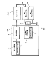
- Another aspect of the electronic apparatus is a semiconductor integrated circuit device having the above-described configuration, a clock generation circuit that generates a clock signal that defines a clock frequency for controlling the semiconductor integrated circuit device, and the monitor And a controller that changes a clock frequency of a clock signal generated by the clock generation circuit in accordance with an output of the circuit.
- the voltage output circuit changes the voltage supplied to the semiconductor memory device in accordance with the characteristics of the memory cell monitored by the monitor circuit, so that the memory cell array of the semiconductor memory device is configured.
- the controller changes the clock frequency of the clock signal so as to respond to this, so that the memory cell of the semiconductor memory device is set to the optimum clock frequency. Can be adjusted to work with. Thereby, the operation of the electronic device can be further speeded up.
- a semiconductor memory device including a memory cell array having a plurality of memory cells, a semiconductor integrated circuit device including a monitor circuit for monitoring characteristics of the memory cells, and the semiconductor A voltage output circuit connected to a memory device and supplying power to the semiconductor memory device, and a controller for changing an output voltage of the voltage output circuit in accordance with an output of the monitor circuit.
- the voltage supplied from the voltage output circuit to the semiconductor memory device by the controller is changed according to the characteristics of the memory cell monitored by the monitor circuit.
- a voltage capable of maintaining the normal characteristics and operation of the semiconductor memory device is supplied to the memory cells constituting the semiconductor memory device even when the threshold voltages of the transistors of the memory cells are manufactured and aged over time. be able to.
- the characteristic of the memory cell in the claims and the specification means a parameter that can be converted into the threshold voltage of the transistor of the memory cell itself or the threshold voltage of the transistor of the memory cell. Specifically, for example, it is a leak current of the memory cell array or a voltage converted value thereof.
- the state of the memory cell in the claims and the specification means a state in which the corresponding memory cell is in a write state (High level) or a read state (Low level).
- the present invention is configured as described above, and does not increase the inspection cost with respect to the memory cells constituting the memory cell array of the semiconductor memory device. As a result, it is possible to supply a voltage capable of maintaining the normal characteristics and operation of the semiconductor memory device even with respect to aging. That is, as a result, the present invention changes the output of the voltage output circuit that supplies power to the memory cell array according to the characteristics of the memory cell monitored by the monitor circuit, for example, during standby of the semiconductor memory device. A power supply voltage that can sufficiently satisfy the leak current characteristics and data retention characteristics of memory cells against manufacturing variations of threshold voltages of memory cell transistors and aging deterioration due to long-term use without increasing the inspection cost. There is an effect that can be supplied.
- the present invention provides a memory without increasing the inspection cost by changing the output of the voltage output circuit according to the characteristics of the memory cell monitored by the monitor circuit, for example, during normal operation of the semiconductor memory device. There is an effect that it is possible to supply the memory cell with a voltage that can provide an appropriate operation margin against manufacturing variations of the threshold voltage of the transistor of the cell and aging deterioration due to long-term use.
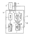
- FIG. 1 is a block diagram showing a schematic configuration of a semiconductor integrated circuit device according to the first embodiment of the present invention.
- FIG. 2 is a circuit diagram showing memory cells constituting the memory cell array of the semiconductor memory device in the semiconductor integrated circuit device shown in FIG.
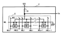
- FIG. 3 is a schematic circuit diagram showing a monitor circuit in the semiconductor integrated circuit device shown in FIG.
- FIG. 4 is a schematic circuit diagram showing a detection circuit in the semiconductor integrated circuit device shown in FIG.
- FIG. 5 is a schematic circuit diagram showing the second voltage output circuit 4b in the semiconductor integrated circuit device shown in FIG.
- FIG. 6 is a schematic circuit diagram showing a detection circuit in the semiconductor integrated circuit device according to the second embodiment of the present invention.
- FIG. 1 is a block diagram showing a schematic configuration of a semiconductor integrated circuit device according to the first embodiment of the present invention.
- FIG. 2 is a circuit diagram showing memory cells constituting the memory cell array of the semiconductor memory device in the semiconductor integrated circuit device shown in FIG.
- FIG. 3 is a schematic circuit diagram
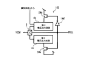
- FIG. 7 is a schematic circuit diagram showing power supply switching means in the semiconductor integrated circuit device according to the third embodiment of the present invention.
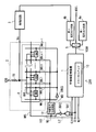
- FIG. 8 is a schematic circuit diagram showing a semiconductor integrated circuit device according to the fourth embodiment of the present invention.
- FIG. 9 is a schematic circuit diagram showing a synchronization signal generating circuit in the semiconductor integrated circuit device shown in FIG.
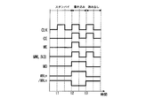
- FIG. 10 is a timing chart of the semiconductor integrated circuit device shown in FIG.
- FIG. 11 is a schematic circuit diagram showing a monitor circuit in a semiconductor integrated circuit device according to the sixth embodiment of the present invention.
- FIG. 12 is a schematic circuit diagram showing a semiconductor integrated circuit according to the sixth embodiment of the present invention.
- FIG. 13 is a block diagram showing a schematic configuration of an electronic apparatus according to the seventh embodiment of the present invention.
- FIG. 14 is a block diagram showing a schematic configuration of an electronic apparatus according to the eighth embodiment of the present invention.
- FIG. 15 is a graph showing the threshold voltage dependency in the memory cell of the semiconductor memory device.
- a transistor is used for a memory cell constituting a memory cell array of the semiconductor memory device.
- an increase in leakage current of transistors has become a problem as the process becomes finer.
- the capacity of the mounted semiconductor memory device tends to increase. Therefore, in the semiconductor integrated circuit device, the power consumption of the memory cell array of the mounted semiconductor memory device is the power consumption of the entire system. It has come to occupy a large percentage of the total. Therefore, it is required to reduce the power consumption of the memory cell array in the semiconductor memory device.
- the power supply voltage of the memory cell becomes lower than a predetermined voltage, the data retention capability of the memory cell is lost and the stored data is erased. Therefore, all the memory cell arrays of the semiconductor memory device are erased. It is necessary to set the voltage in a range higher than the voltage at which the memory cell can hold data.
- FIG. 15 is a graph showing the threshold voltage dependence of the memory cell voltage of the semiconductor memory device.
- a characteristic a (a0, a1) shown in FIG. 15 is a threshold voltage dependency of the leak characteristic of the memory cell for satisfying the product standard with respect to the leak current, and a characteristic b is a data retention characteristic of the memory cell. Threshold voltage dependence.
- the power supply voltage of the memory cell needs to be lower than the characteristic a, and in order to hold data at a lower voltage, the memory The power supply voltage of the cell needs to be higher than the characteristic b.
- the threshold voltages Vth1 and Vth2 indicate corner conditions that define the amount of manufacturing variation in the threshold voltage of the transistor. That is, the threshold voltage of the memory cell transistor can be different between Vth1 and Vth2 due to manufacturing variations.
- the leakage current characteristic a shifts from a0 to a1 on the low voltage side due to an increase in the leakage current of the transistor accompanying the miniaturization of the memory cell array and the further demand for lower power consumption of the product. Therefore, it becomes difficult to set the power supply voltage of the memory cell to a fixed voltage that does not depend on the threshold voltage of the transistor of the memory cell.
- the power supply voltage of the memory cell can be set to the fixed voltage V1, but a problem may occur due to manufacturing variations in the threshold voltage of the transistor.
- a margin can be obtained with respect to the lower limit value of the data holding voltage for the data holding characteristic b, but there is no margin for the leakage current characteristic a1 and manufacturing variation. If the threshold voltage of the transistor becomes lower than Vth1 due to deterioration over time, the leakage current characteristics may not be satisfied. Further, in a transistor manufactured with a threshold voltage near Vth2, a margin can be obtained for the leakage current characteristic a1 with respect to the upper limit value of the leakage current voltage, but there is no margin for the data retention characteristic b, resulting in manufacturing variations. If the threshold voltage becomes higher than Vth2 due to deterioration over time, the data retention characteristics may not be satisfied.
- the voltage characteristic V2 shown in FIG. As described above, it is effective to increase the power supply voltage to be supplied as the threshold voltage of the transistor increases, and it is effective to lower the power supply voltage to be supplied as the threshold voltage of the transistor decreases.
- the semiconductor integrated circuit device and the electronic device monitor the finish of the threshold voltage of the transistor of the memory cell inside the semiconductor integrated circuit device and the electronic device, and respond to the monitoring result.
- the leakage current characteristics and data retention characteristics are fully satisfied without increasing the inspection cost, even for characteristic variations due to manufacturing variations and characteristics variations due to long-term use. Can be supplied.
- FIG. 1 is a block diagram showing a schematic configuration of a semiconductor integrated circuit device according to the first embodiment of the present invention.
- the semiconductor integrated circuit device 100 includes a semiconductor memory device 1 including a memory cell array 10 having a plurality of memory cells, as shown in FIG.
- the semiconductor integrated circuit device 100 further includes a voltage output circuit that outputs a power supply voltage to the memory cell array 10 of the semiconductor memory device 1.
- the voltage output circuit includes first and second voltage output circuits 4a and 4b having different output voltages. The first and second voltage output circuits 4a and 4b are selectively connected to the semiconductor memory device 1 via the switching circuit 5, and the connected first or second voltage output circuits 4a and 4b are connected to the semiconductor memory device 1. A power supply voltage is supplied to the memory cell array 10.
- the switching circuit 5 connects one of the first or second voltage output circuits 4a and 4b to the memory cell array 10 of the semiconductor memory device 1 in accordance with an external mode selection signal MSEL. Specifically, the switching circuit 5 connects the memory cell array 10 of the semiconductor memory device 1 and the first voltage output circuit 4a when the semiconductor memory device 1 is in the normal operation mode (referred to as a first mode). When the memory device 1 is in the standby mode, the memory cell array 10 of the semiconductor memory device 1 and the second voltage output circuit 4b are connected (referred to as a second mode).
- the output voltage of the second voltage output circuit 4b is configured to be lower than the output voltage of the first voltage output circuit 4a.
- a configuration including two voltage output circuits 4a and 4b having different output voltages is illustrated, but the present invention can change the power supply voltage supplied to the semiconductor memory device 1.
- the present invention is not limited to this as long as it has a possible voltage output circuit, and the power supply voltage supplied to the semiconductor memory device 1 may be changed as appropriate in one voltage output circuit.
- the semiconductor integrated circuit device 100 includes a monitor circuit 2 that monitors the characteristics of the memory cell array 10 of the semiconductor memory device 1.
- the output of the monitor circuit 2 is detected by the detection circuit 3 and digitized.
- the digitized output of the monitor circuit 2 is input to the second voltage output circuit 4b.
- the output voltage of the second voltage output circuit 4b is set according to the digitized output of the monitor circuit 2 (that is, the output of the detection circuit 3).
- the output voltage of the second voltage output circuit 4b changes in accordance with the change in the output.
- the power supply voltage of the memory cell array 10 when the semiconductor memory device 1 is in the standby mode is configured to be set inside the semiconductor integrated circuit in accordance with the manufacturing variation of the threshold voltage of the transistor of the memory cell.
- power supply voltage control according to the threshold voltage of the memory cell transistor without increasing the inspection cost, even for manufacturing variations in the threshold voltage of the memory cell transistor and aging deterioration due to continuous use. Can be performed with high accuracy. Therefore, it is possible to supply a power supply voltage that sufficiently satisfies the leakage current characteristic and the data retention characteristic even with respect to manufacturing variations and aging deterioration of the threshold voltage of the transistor of the memory cell.
- the characteristics of the memory cell may be any parameter that can be converted into the threshold voltage of the memory cell transistor itself or the threshold voltage of the memory cell transistor, and the detected value may be a current value. It may be a voltage value.
- FIG. 2 is a circuit diagram showing memory cells constituting the memory cell array of the semiconductor memory device in the semiconductor integrated circuit device shown in FIG.
- the memory cell MC in the present embodiment is a holding circuit (CMOS type) that operates a CMOS circuit having two P-type MOS transistors QP1 and QP2 and two N-type MOS transistors QN3 and QN4 with two N-type MOS transistors QN1 and QN2.
- SRAM memory cell CMOS type
- CMOS type complementary MOS transistors
- the present invention is not limited to this as long as it is a field effect transistor in which leakage current is a problem.
- a junction type field effect transistor may be used.
- the memory cell MC is constituted by a complementary CMOS circuit, the circuit may be constituted by only P-type or N-type transistors.
- the source terminals of the P-type MOS transistors QP1 and QP2 are both connected to the power supply line VDDM.
- the drain terminals of P-type MOS transistors QP1 and QP2 are connected to the drain terminals of N-type MOS transistors QN3 and QN4, respectively.
- the source terminals of the N-type MOS transistors QN3 and QN4 are all grounded.
- the drain terminals of the N-type MOS transistors QN1, QN2 are connected to complementary bit line pairs BL, / BL for reading or writing data held in the memory cells MC, respectively.
- the source terminal of the N-type MOS transistor QN1 is connected to the drain terminals of the P-type MOS transistor QP1 and the N-type MOS transistor QN3, and the source terminal of the N-type MOS transistor QN2 is connected to the P-type MOS transistor QP2 and the N-type MOS transistor QN4. Connected to the drain terminal.
- the gate terminals of the N-type MOS transistors QN1 and QN2 are all connected to a word line WL that selects one of the plurality of memory cell MC columns.
- connection node of the drain terminals of the P-type MOS transistor QP1 and the N-type MOS transistor QN3 and the source terminal of the N-type MOS transistor QN3 is the storage node N1 of the memory cell MC
- a connection node between the drain terminal of QN4 and the source terminal of the N-type MOS transistor QN2 is a storage node N2 of the memory cell MC.
- the storage node N1 is connected to the gate terminals of the P-type MOS transistor QP2 and the N-type MOS transistor QN4, and the storage node N2 is connected to the gate terminals of the P-type MOS transistor QP1 and the N-type MOS transistor QN3.
- the word line WL In the normal operation mode, when the word line WL is at a high level, the N-type MOS transistors QN1 and QN2 of the corresponding memory cell MC are turned on, and are connected to the storage nodes N1 and N2 via the complementary bit line pair BL and / BL. Data is read or written. On the other hand, in the standby mode, the word line WL is set to the low level, and the N-type MOS transistors QN1 and QN2 of the memory cell MC are turned off, so that the data of the storage nodes N1 and N2 are held as they are.
- the memory cell array 10 of the semiconductor memory device 1 is configured by arranging a plurality of the memory cells MC.
- the memory cell array unit 6 of the monitor circuit 2 includes at least one memory cell having the same configuration as the memory cell included in the memory cell array 10 of the semiconductor memory device 1. Then, the characteristics of the memory cells in the memory cell array 10 of the semiconductor memory device 1 are indirectly detected by detecting the characteristics of the memory cells in the memory cell array section 6 of the monitor circuit 2 (leakage current described later in this embodiment). To do.
- FIG. 3 is a schematic circuit diagram showing a monitor circuit in the semiconductor integrated circuit device shown in FIG.
- the memory cells constituting the memory cell array unit 6 of the monitor circuit 2 are indicated as MMC for convenience, but the memory cells MMC have the same configuration as the memory cells MC of the semiconductor memory device 1 shown in FIG. Have.
- the n memory cells MMC are connected to the monitor circuit word line MWL and the monitor circuit complementary bit line pair MBLn, / MBLn. That is, the source terminals of the P-type MOS transistors QP1 and QP2 in the memory cell MC shown in FIG. 2 are both connected to the monitor circuit power supply line MVL, and the gate terminals of the N-type MOS transistors QN1 and QN2 are both the monitor circuit word. Connected to line MWL. Further, the drain terminals of the N-type MOS transistors QN1 and QN2 are connected to the corresponding complementary bit line pairs MBLn and / MBLn for the monitor circuit, respectively.
- the present invention statistically monitors the characteristics of the memory cells MC of the semiconductor memory device 1 from the characteristics of each of the plurality of memory cells MMC, the number of memory cells MMC in the memory cell array unit 6 is the same as that of the semiconductor memory. Although the number may be the same as or different from the number of memory cells MC of the device 1, it is preferable to connect as many memory cells MMC as possible in order to detect the characteristics of the memory cells MC with high accuracy.
- the monitor circuit 2 is provided to adjust the power supply voltage of the memory cell array 10 when the semiconductor memory device 1 is in the standby mode. Therefore, each memory cell MMC in the memory cell array unit 6 is Biased to maintain data retention. That is, the word line MWL is fixed to the Low level, and all the complementary bit line pairs MBLn, / MBLn are fixed to the High level.
- the monitor circuit 2 has a resistance element R1 which is a resistance portion having one end connected to the external power supply VDD and the other end connected to the power supply line MVL of the memory cell array portion 6. That is, power supplied from the external power supply VDD is supplied to the monitor circuit power supply line MVL of the memory cell array unit 6 via the resistance element R1.
- the monitor circuit 2 is provided to monitor the threshold voltage of the transistors in the memory cell array unit 6, but in the present embodiment, the voltage value Vm is output from the node on the other end side of the resistor element R1 to the detection circuit 3. Is configured to do. Thereby, the monitor circuit 2 outputs the voltage drop of the resistance element R1 with respect to the power supply voltage of the external power supply VDD as the output voltage Vm.
- FIG. 4 is a schematic circuit diagram showing a detection circuit in the semiconductor integrated circuit device shown in FIG.
- the detection circuit 3 is a circuit that detects the output voltage Vm due to the leakage current output from the monitor circuit 2, digitizes it, and outputs it to the second voltage output circuit 4b.
- the number n of comparators CAn to be connected is the number of bits n of the output digital value.
- the detection circuit 3 is configured such that the output Vm of the monitor circuit 2 and the reference voltage Vref (n) are input to the input terminals of the comparator CAn.
- the reference voltage Vref (n) is a predetermined fixed voltage.
- the plurality of reference voltages Vref (n) all have different voltages. That is, for example, Vref (0)> Vref (1)>...> Vref (n ⁇ 1).
- the value and number of the reference voltage Vref (n) are arbitrarily set according to the assumed characteristics of the memory cell MC.
- each of the comparators CAn compares the input output voltage Vm of the monitor circuit 2 with the reference voltage Vref (n), and outputs the result to the output terminal Qn of the comparator CAn.
- the output terminal Qn of the comparator CAn outputs a high level when the output Vm of the monitor circuit 2 is higher than the reference voltage Vref (n). That is, the output of the output terminal Qn is an n-bit output obtained by digitizing the analog output Vm of the monitor circuit 2.
- Vref (0)> Vref (1)>...> Vref (3)> Vm> Vref (4)>...> Vref (n ⁇ 1) the comparators CA0 to CA3 have the output voltage Vm as the reference.
- the second voltage output circuit 4b can be adjusted easily and in multiple stages.
- FIG. 5 is a schematic circuit diagram showing the second voltage output circuit 4b in the semiconductor integrated circuit device shown in FIG.
- the second voltage output circuit 4b is configured to change the output voltage in accordance with the output of the monitor circuit 2.
- the second voltage output circuit 4b has a variable resistor R2 that divides the voltage applied according to the output of the monitor circuit 2, and changes the output voltage according to the voltage dividing ratio of the variable resistor R2. It is configured as follows.
- variable resistor R2 receives the output Qn of the detection circuit 3 obtained by digitizing the output Vm of the monitor circuit 2, and the variable resistor R2 divides the output Vm into the voltage dividing ratio r2 / r1 based on the output Qn.
- the second voltage output circuit 4b further compares and amplifies the reference voltage generation circuit 7 for generating a reference voltage and the voltage Vd divided by the variable resistor R2 based on the reference voltage generated by the reference voltage generation circuit 7.
- a differential amplifier 8 and an output transistor 9 that operates based on the output of the differential amplifier 8 are provided.
- the output transistor 9 is interposed between the power supply and the variable resistor R2.
- the output transistor 9 shown in FIG. 5 is an N-type MOS transistor, but the present invention is not limited to this, and may be, for example, a P-type MOS transistor or a junction type transistor.
- An output terminal VO is connected to a node between the output transistor 9 and the variable resistor R2, and a voltage output from the output terminal VO is a power supply voltage supplied to the semiconductor memory device 1.
- the differential amplifier 8 controls the operation of the output transistor 9 according to the voltage Vd. For example, when the leakage current increases in the memory cell array unit 6 of the monitor circuit 2, the voltage Vm input to the detection circuit 3 decreases, and the voltage dividing ratio r2 / r1 increases. As a result, the divided voltage Vd is increased, and the output voltage of the differential amplifier 8 (the gate voltage of the output transistor 9) is decreased.
- the voltage dividing ratio r2 / r1 of the variable resistor R2 is set in advance so that a voltage equal to or higher than a lower limit voltage capable of holding data in the memory cell MC is output from the output terminal VO.
- variable output regulator is used for such a voltage output circuit.
- the output Qn of the detection circuit 3 is analogized by a D / A conversion circuit (not shown) and then input to the variable resistor R2, but the present invention is not limited to this.
- the variable resistor R2 one variable resistor unit having one input is used for the n-bit output of the detection circuit 3, but as long as the divided voltage Vd is obtained.
- the present invention is not limited to this, and for example, a plurality of resistance units to which the output of the detection circuit 3 is input bit by bit may be provided.
- the first voltage output circuit 4a has substantially the same configuration as the second voltage output circuit 4b. However, since the second voltage output circuit 4a supplies a constant power supply voltage to the semiconductor memory device 1, it does not have the variable resistor R2 (or the voltage dividing ratio is fixed in the variable resistor R2). Further, since the power supply voltage output from the first voltage output circuit 4a is larger than the power supply voltage output from the second voltage output circuit 4b, the size of the output transistor 9 is larger than that applied to the second voltage output circuit 4b. It is preferable.
- the switching circuit 5 is configured as a power supply switching means for switching the voltage output circuits 4a and 4b connected to the semiconductor memory device 1 by a mode selection signal MSEL that changes according to the operation mode of the semiconductor memory device 1. That is, for example, when the semiconductor memory device 1 is in the normal operation mode, the mode selection signal MSEL becomes High level, and the switching circuit 5 switches so as to connect the semiconductor memory device 1 and the first voltage output circuit 4a. Further, when the semiconductor memory device 1 enters the standby mode, the mode selection signal MSEL becomes the low level, and the switching circuit 5 switches so as to connect the semiconductor memory device 1 and the second voltage output circuit 4b.
- a mode selection signal MSEL that changes according to the operation mode of the semiconductor memory device 1. That is, for example, when the semiconductor memory device 1 is in the normal operation mode, the mode selection signal MSEL becomes High level, and the switching circuit 5 switches so as to connect the semiconductor memory device 1 and the first voltage output circuit 4a. Further, when the semiconductor memory device 1 enters the standby mode, the mode selection signal MSEL becomes the
- the threshold value of the memory cell transistor without increasing the inspection cost for the memory cell MC constituting the memory cell array 10 of the semiconductor memory device 1. It is possible to supply a power supply voltage that can sufficiently satisfy leakage current characteristics and data retention characteristics even with respect to voltage manufacturing variations and aging degradation.
- FIG. 6 is a schematic circuit diagram showing a detection circuit in the semiconductor integrated circuit device according to the second embodiment of the present invention. Since the configuration other than the detection circuit is the same as that of the first embodiment, the description thereof is omitted.
- the holding circuit LAn is configured by a logic circuit unit L1 configured by a combination of logic circuits.
- the holding circuit LAn is not particularly limited as long as it has a configuration that can hold input data until a predetermined time.
- the comparator CBn is configured to determine the output by a predetermined first signal, and the holding circuit 103 outputs the output from the comparator CBn at that time by a second signal sent after a predetermined time has elapsed from the first signal. It is configured to capture and retain data.
- the second signal is a signal generated from the first signal (in this embodiment, a signal common to the first signal), and is delayed for a predetermined time after the first signal reaches the comparator CBn.
- the second signal reaches the holding circuit LAn.
- the first signal is a reset signal RST input to the semiconductor memory device when the power is turned on, and the detection circuit 103 is connected to an input terminal to which the reset signal RST is input and each of the comparators CBn.
- the input terminal and the logic circuit unit L1 are configured to be connected via the delay buffer 11.
- the reset signal RST generated when the power is turned on is input to the detection circuit 103.
- the reset signal RST input to the detection circuit 103 is input to each of the comparators CBn as a first signal.
- the comparator CBn compares the output voltage Vm of the monitor circuit 2 with each reference voltage Vref (n) and determines the output.
- the reset signal RST is also input to the delay buffer 11, and after a predetermined time (reset time) determined by the delay time of the delay buffer 11 has elapsed, the reset signal RST is input to the logic circuit unit L1 as the second signal.
- the holding circuit LAn takes in the output data of the corresponding comparator CBn and holds it.
- the holding circuit LAn digitizes and holds the output Vm of the monitor circuit 2 after the reset time has elapsed since the comparator CBn received the reset signal RST. Accordingly, the output Qn of the detection circuit 103 continues to be output at the same value until the next reset signal RST is received.
- the output state in the monitor circuit 2 may be unstable.
- the output voltage Vm of the monitor circuit 2 is acquired at such timing and the power supply voltage supplied to the semiconductor memory device 1 by the second voltage output circuit 4b is changed based on this, the supplied power supply voltage is not stabilized. There is a possibility that a voltage that does not satisfy the leakage current characteristic and the data retention characteristic of the memory cell MC is supplied.
- the semiconductor memory is based on the voltage value when the second signal is sent after a lapse of a predetermined time after the first signal is sent.
- the output of the monitor circuit 2 when the output characteristics of the monitor circuit 2 are not stable immediately after the power is turned on is used as a reference for changing the power supply voltage supplied to the semiconductor memory device 1. Therefore, stable power supply can be performed to the semiconductor memory device.
- the signal wiring can be effectively used and the circuit configuration can be simplified.
- FIG. 7 is a schematic circuit diagram showing power supply switching means in the semiconductor integrated circuit device according to the third embodiment of the present invention. Since the configuration other than the power supply switching unit is the same as that of the first embodiment, the description thereof is omitted.
- the power supply switching means 105 in this embodiment includes a switching circuit 5 similar to that in the first embodiment, an external power supply that supplies power to each of the first and second voltage output circuits 4a and 4b, and the first and second power supplies.
- Switching elements SWa and SWb are provided between the voltage output circuits 4a and 4b.
- the switch elements SWa and SWb are configured to be selectively turned on in response to the mode selection signal MSEL.
- N-type MOS transistors are used as the switch elements SWa and SWb, respectively.
- any element that can interrupt power supply such as a P-type MOS transistor or a junction field effect transistor, is used. It does n’t matter.
- An external power supply is connected to the source terminals of the switch elements SWa and SWb, and the first and second voltage output circuits 4a and 4b are connected to the drain terminals.
- the mode selection signal MSEL is input to one of the gate terminals of the switch elements SWa and SWb (here, the switch element SWa), and the other of the switch elements SWa and SWb (here, the switch element SWb) receives the mode selection signal MSEL. Inverted input is input.
- the inverter INV1 is connected to the other gate terminal of the switch elements SWa and SWb.
- the mode selection signal MSEL is at a high level, and the switching circuit 5 is connected to the semiconductor memory device 1 and the first voltage output circuit. Switch to the first mode to connect 4a.
- the switch element SWa is turned on and the switch element SWb that switches the power supply to the second voltage output circuit 4b. Is turned to Low level by the inverter INV1, so that the switch element SWb is turned off.
- power is supplied only to the first voltage output circuit 4a that supplies power to the semiconductor memory device 1, and power supply to the second voltage output circuit 4b is blocked.
- the mode selection signal MSEL becomes the low level
- the switching circuit 5 switches to the second mode in which the semiconductor memory device 1 and the second voltage output circuit 4b are connected.
- the switch element SWa is turned off when the gate terminal of the switch element SWa becomes Low level
- the switch element SWb is turned on when the gate terminal of the switch element SWb becomes High level by the inverter INV1.
- power is supplied only to the second voltage output circuit 4b that supplies power to the semiconductor memory device 1, and power supply to the first voltage output circuit 4a is blocked.
- FIG. 8 is a schematic circuit diagram showing a semiconductor integrated circuit device according to the fourth embodiment of the present invention.
- the present embodiment is different from the first embodiment in that it includes a monitor circuit control unit 102 that switches the state of the memory cell MMC constituting the memory cell array unit 6 of the monitor circuit 2 to a low level or a high level.
- the monitor circuit control unit 102 in the present embodiment is configured to switch the state of the memory cell MMC of the memory cell array unit 6 to a low or high level based on a control signal of the semiconductor memory device 1.
- the control signal of the semiconductor memory device 1 includes a clock signal CLK defining a clock frequency for controlling the semiconductor memory device, a chip enable signal CE for switching the operation mode of the semiconductor memory device 1, and a write operation by the semiconductor memory device. Or a write enable signal WE for switching between read and write operations. That is, the semiconductor memory device 1 is a synchronous semiconductor memory device that operates in synchronization with the clock signal CLK.
- These control signals CLK, CE, and WE are control signals sent from, for example, a main controller of an electronic device (not shown) on which the semiconductor integrated circuit device 200 according to this embodiment is mounted.
- the semiconductor memory device 1 is configured to be in the normal operation mode when the chip enable signal CE is at the high level and in the standby mode when the chip enable signal CE is at the low level. Further, in the normal operation mode, the semiconductor memory device 1 is configured to perform a read operation when the write enable signal WE is at a low level and perform a write operation when the write enable signal WE is at a high level.
- the monitor circuit control unit 102 is configured to switch the state of the memory cell MMC of the memory cell array unit 6 to the Low or High level according to the chip enable signal CE in synchronization with the clock signal CLK.
- the monitor circuit control unit 102 includes a logic circuit unit L2 in which the monitor circuit word line MWL is at a high level when both the clock signal CLK and the chip enable signal CE are at a high level, and a memory And a synchronization signal generation circuit 12 for generating a synchronization signal for synchronizing the monitor circuit complementary bit line pair MBLn, / MBLn of the cell array section 6 with the monitor circuit word line MWL.
- the logic circuit unit L2 includes a NAND circuit NA1 to which the clock signal CLK and the chip enable signal CE are input, and an inverter INV2 that inverts and outputs the output of the NAND circuit NA1.
- the NAND circuit NA1 and the inverter INV2 form an AND circuit, but an existing AND circuit may be applied.
- the synchronization signal generation circuit 12 has an input side connected to the branch node N3 on the output side of the logic circuit unit L2, and an output side connected to each of the monitor circuit bit lines MBLn.
- the output side of the synchronization signal generation circuit 12 is also connected to each of the inverted bit lines / MBLn for the monitor circuit via the inverter INV3.
- the output of the synchronization signal generation circuit 12 that is, the complementary bit line pair MBLn for the monitor circuit of the memory cell array unit 6 is obtained.
- / MBLn is inverted, the memory state of the memory cell MMC can be inverted.
- the same write operation as that of the memory cell MC of the semiconductor memory device 1 is performed according to the output of the synchronization signal generation circuit 12.
- FIG. 9 is a schematic circuit diagram showing a synchronization signal generating circuit in the semiconductor integrated circuit device shown in FIG.
- the synchronization signal generation circuit 12 includes a loop circuit unit P1 having a plurality of inverters, first and second holding circuit units LB1 and LB2 inserted in the loop circuit unit, and a loop circuit unit.
- First and second switch sections G1 and G2 are provided for controlling data input to the first and second holding circuits according to the state of the word line MWL.
- the loop circuit unit P1 is connected in series to a NAND circuit NA2 to which a feedback output is input through a power supply voltage and a feedback path from the second holding circuit, and a loop circuit from the output of the NAND circuit NA2 to the input of the NAND circuit NA2. It has an even number of inverters INV4 to INV11.
- the NAND circuit NA2 since one input is the power supply voltage, one input is always at the High level, and therefore, the NAND circuit NA2 operates as an inverter that inverts the feedback output. That is, the loop circuit unit P1 operates as a ring oscillator composed of an odd number of inverters.
- the first and second holding circuit units LB1 and LB2 include inverters INV5 and INV7, which are components of the ring oscillator, and inverters INV12 and INV13 connected in parallel to the inverters INV5 and INV7, respectively.
- the outputs of the inverters INV5 and INV7 are input to the inverters INV12 and INV13, and the outputs of the inverters INV12 and INV13 are input to the inverters INV5 and INV7.
- the first and second holding circuit units LB1 and LB2 invert and output the input signal and hold the state.
- the first and second switch parts G1 and G2 are each constituted by a transfer gate, and the first and second holding circuit parts LB1 and LB2 are connected to the output side of the transfer gate, respectively.
- Complementary inputs from the branch node N3 are input to the gate terminals of the first and second switch sections G1 and G2 by the two inverters INV14 and 15. More specifically, the second switch unit G2 is turned off when the first switch unit G1 is on, and the second switch unit G2 is turned on when the first switch unit G1 is off.
- the output side of the second holding circuit unit LB2 includes a feedback path in which four inverters INV8 to 11 which are components of the ring oscillator are connected in series, and an inverter that inverts and outputs the output of the second holding circuit unit LB2. Branches to the output path to which the INV 16 is connected.
- the output of the inverter INV11 in the feedback path is input to the NAND circuit NA2 as a feedback output.
- the output signal MD output from the output path becomes write data to the memory cell MMC of the memory cell array unit 6.
- the synchronization signal generation circuit 12 having the above configuration will be described.
- the signal level of the monitor circuit word line MWL is low
- the low level is input from the branch node N3 to the synchronization signal generation circuit 12.
- the first switch part G1 is turned on, and the second switch part G2 is turned off.
- the signal level of the previous output signal MD is Low
- the High level is input to the NAND circuit NA2
- the Low level is output
- the NAND circuit NA2 outputs the Low level to the first holding circuit unit LB1 via the inverter INV4.
- the High level is input.
- the first holding circuit unit LB1 holds a low level in order to hold the input signal in an inverted state.
- the first holding circuit LB1 holds the signal level of the previous output signal MD.
- the first switch part G1 is turned off and the second switch part G2 is turned on.
- the information held in the first holding circuit unit LB1 is inverted by the inverter INV6 and then input to the second holding circuit LB2.
- the first holding circuit LB1 holds the Low level as in the above example
- the High level is input to the second holding circuit LB2
- the second holding circuit LB2 is in its inverted state, the Low level. Hold.
- the output signal MD at this time becomes a high level inverted by the inverter INV16.
- the first switch part G1 is turned on and the second switch part G2 is turned off.
- the signal level of the output signal MD is held in the first holding circuit unit LB1.
- the second holding circuit LB2 holds the state before the signal level of the word line MWL becomes the Low level. That is, as in the above-described example, when the signal level of the output signal MD is High level before the signal level of the monitor circuit word line MWL becomes Low level, the first holding circuit unit LB1 becomes High level. The second holding circuit unit LB2 holds the Low level. Therefore, the output signal MD is held at a high level.
- the signal level of the word line MWL becomes high again, the information held in the first holding circuit unit LB1 is inverted by the inverter INV6 and input to the second holding circuit LB2 as described above. Therefore, the signal level of the output signal MD is held in an inverted state.
- the signal level of the output signal MD is inverted only when the signal level of the monitor circuit word line MWL changes from the low level to the high level.
- the signal level of the output signal MD is not inverted, and is maintained until the signal level of the monitor circuit word line MWL changes to the High level next time. Is done.
- FIG. 10 is a timing chart of the semiconductor integrated circuit device shown in FIG.
- the clock signal CLK, the chip enable signal CE, and the write enable signal WE are assumed to be at a low level.
- the monitor circuit word line signal MWL in the memory cell array section 6 is at the low level.
- the output signal MD of the synchronization signal generation circuit 12 can take an arbitrary level.
- the monitor circuit bit line signal MBLn of the memory cell array unit 6 is at the Low level.
- the inversion bit line / MBLn for the monitor circuit in the memory cell array unit 6 is at a high level.
- the clock signal CLK becomes High level for a predetermined period from time t1, t2, t3.
- the semiconductor memory device 1 is in a standby mode in which no read operation or write operation is performed in the memory cell MC.
- the signal level of the branch node N3, which is the output of the logic circuit portion L2 is low, and therefore the signal level of the monitor circuit word line MWL is low.
- the memory cell array section 6 is in a state substantially equal to the state of the memory array section 6 in the first embodiment in which the signal level of the monitor circuit word line MWL is fixed at the low level.
- the signal level of the output signal MD of the synchronization signal generation circuit 12 is the low level that is the initial state.
- the semiconductor memory device 1 enters the normal operation mode.
- the write enable signal WE is also at the high level
- the write operation mode is set.
- the signal level of the branch node N3, which is the output of the logic circuit portion L2 is at a high level, and therefore the monitor circuit word line MWL is at a high level.
- the signal level of the output signal MD of the synchronization signal generation circuit 12 is inverted and changes from the initial low level to the high level.
- the complementary bit line pair MBLn, / MBLn of the memory cell array unit 6 is inverted, and the data held in the memory cell MMC constituting the monitor circuit 2 is rewritten. Thereafter, the clock signal CLK, the chip enable signal CE, and the write enable signal WE transition to the low level, so that the signal level of the word line MWL transitions to the low level.
- the signal level of the output signal MD of the synchronization signal generation circuit 12 is High level is maintained.
- the semiconductor memory device 1 enters the read operation mode.
- the signal level of the branch node N3 that is the output of the logic circuit portion L2 becomes High level, and therefore the signal level of the word line MWL becomes High level.
- the signal level of the output signal MD of the synchronization signal generation circuit 12 is inverted and transitions from the High level to the Low level.
- the complementary bit line pair MBLn, / MBLn for the monitor circuit in the memory cell array unit 6 is inverted, and the data held in the memory cell MMC constituting the monitor circuit 2 is rewritten.
- the clock signal CLK, the chip enable signal CE, and the write enable signal WE transition to the low level, so that the word line MWL transitions to the low level.
- the signal level of the output signal MD of the synchronization signal generation circuit 12 is the low level. Maintained.
- the memory cell array 10 of the semiconductor memory device is in a data holding state in which the voltage level of the word line and the complementary bit line pair is constant in the standby mode, but the voltage level of the word line and the complementary bit line pair is the memory level in the operation mode. Each time the cell is accessed, it will change repeatedly. The characteristics of a memory cell in which such a change in voltage level is continuously performed after long-term use may be different from the characteristics of a memory cell holding a certain voltage level.
- the semiconductor integrated circuit device of this embodiment as described above, every time the access to the semiconductor memory device is performed and the monitor circuit word line MWL becomes High level, the memory cell array of the monitor circuit 2 is used. The state of the memory cell MMC in the unit 6 is rewritten to the Low or High level. For this reason, the characteristic change caused by the long-term use of the memory cell MMC of the monitor circuit 2 can be brought close to the characteristic change of the memory cell MC of the semiconductor memory device 1. Can be monitored.
- FIG. 11 is a schematic circuit diagram showing a monitor circuit in the semiconductor integrated circuit device according to the sixth embodiment of the present invention. Since the configuration other than the monitor circuit is the same as that of the first embodiment, the description thereof is omitted.
- the monitor circuit 302 has a resistance element R1 which is a resistance part having one end connected to the external power supply VDD and the other end connected to the power supply line MVL of the memory cell array part 6, and in parallel with the resistance element R1. And a connected switch element SWc.
- the switch element SWc shown in FIG. 11 is configured by an N-type MOS transistor.
- a source terminal and a drain terminal are connected to both ends of the resistor element R1.
- a mode selection signal MSEL is input to the gate terminal of the switch element SWc.
- the switch element SWc in the present embodiment is configured by an N-type MOS transistor, the present invention is not limited to this as long as it can be switched on / off according to the mode selection signal.
- other transistor elements such as a P-type MOS transistor may be used, and other switch elements may be used.
- the mode selection signal MSEL when the semiconductor memory device 1 is in the standby mode, the mode selection signal MSEL is at the low level, and when the semiconductor memory device 1 is in the normal operation mode, the mode selection signal MSEL is High. Become a level. Therefore, the switch element SWc is turned off when the semiconductor memory device 1 is in the standby mode, and is turned on when the semiconductor memory device 1 is in the normal operation mode.
- the switch element SWc When the semiconductor memory device 1 is in the standby mode, the switch element SWc is turned off, so that the power supply voltage of the memory cell array unit 6 is supplied with the power supply voltage dropped by the resistor element R1 from the external power supply VDD. In other words, the state is the same as in the first embodiment, and the monitor circuit 2 outputs the voltage conversion value of the leakage current as the output Vm.
- the semiconductor memory device 1 enters the normal operation mode and the switch element SWc is turned off, both ends of the resistor element R1 are short-circuited, and the power supply voltage from the external power supply VDD is directly supplied to the power supply of the memory cell array section 6.
- the resistance element R1 for detecting the leakage current is interposed between the external power supply VDD and the memory cell array unit 6, the voltage lower than the power supplied to the memory cell array 10 of the semiconductor memory device 1 is lower than the memory cell array of the memory circuit 2. It is always supplied to the power supply of the unit 6.
- the characteristics of the memory cell to which the power supply voltage lower than the voltage of the external power supply is supplied are different from the characteristics of the memory cell MC of the memory array 10 to which the power supply voltage of the external power supply is directly supplied by long-term use. There is a possibility that accurate monitoring cannot be performed.
- the semiconductor integrated circuit device of the present embodiment in the normal operation mode in which the first voltage output circuit 4a sharing the steady voltage is connected to the power supply line of the memory array of the semiconductor memory device, the external power supply VDD and the memory Since the cell array unit 6 is short-circuited, the voltage supplied to the memory cell MMC of the memory cell array unit 6 can be made equal to the voltage supplied to the memory cell MC of the semiconductor memory device 1, and as a result, due to long-term use.
- the power supply voltage of the memory cell MC of the semiconductor memory device 1 can be controlled systematically even with respect to characteristic deterioration.
- the write assist circuit that improves the write characteristics and the read assist that improves the read characteristics according to the finish of the threshold value of the transistor constituting the memory cell.
- An assist circuit such as a circuit is installed. Although the detailed principle is not described here, these assist circuits expand the operation margin of the semiconductor memory device by supplying an auxiliary voltage different from the operation voltage of the semiconductor integrated circuit device to the memory cell array power supply.
- the test device outside the semiconductor integrated circuit device is used to monitor the finish of the threshold voltage of the transistors constituting the memory cell, and according to the monitoring result, Similarly, a technique for programming the setting of assist conditions by a test apparatus outside the semiconductor integrated circuit device is known.
- the present embodiment is different from the first embodiment in that the power supply voltage of the memory cell array 10 of the semiconductor memory device is changed according to the output of the monitor circuit during the write operation of the semiconductor memory device, and the read operation of the semiconductor memory device is performed.
- the word line voltage of the memory cell array 10 of the semiconductor memory device is configured to be changed according to the output of the monitor circuit.
- FIG. 12 is a schematic circuit diagram showing a semiconductor integrated circuit according to the sixth embodiment of the present invention.
- the voltage output circuit in this embodiment includes first and second voltage output circuits 4a and 4b, and is configured to be selectively connected to the semiconductor memory device 1 by the switching circuit 5.
- the second voltage output circuit 4b is configured to change the output voltage in accordance with the output of the monitor circuit 2, as in the first embodiment.
- the first voltage output circuit 4a of the present embodiment outputs a normal voltage, and the output voltage is supplied to the power supply of the memory cell array 10 of the semiconductor memory device 1 through a write assist circuit described below. .
- the output of the second voltage output circuit 4b and the output of the first voltage output circuit 4a via the write assist circuit are selectively switched by the switching circuit 5 and supplied to the memory cell array 10.
- the write when the memory cell array 10 of the semiconductor memory device 1 is in the write operation mode, the write that adjusts the power supply voltage supplied from the first voltage output circuit 4a according to the output of the detection circuit 3
- An assist circuit unit 104a having a support circuit WA and a read support circuit RA that adjusts the word line voltage of the semiconductor memory device 1 according to the output of the detection circuit 3 when the memory cell array 10 of the semiconductor memory device 1 is in the read operation mode. It has.
- the write assist circuit WA of the assist circuit unit 104a has an input terminal connected to the output terminal of the first voltage output circuit 4a, an output terminal connected to the input terminal of the switching circuit 5, and the memory cell array 10 via the switching circuit 5. Connected to the power line VDDM.
- the write assist circuit WA includes an output voltage adjustment terminal TW, and the output of the detection circuit 3 is input to the output voltage adjustment terminal TW.
- the write support circuit WA is configured to receive a write support circuit activation signal WAS that is generated based on an input signal of the semiconductor memory device 1 and that outputs a voltage adjusted from the write support circuit WA. ing.
- the write support circuit WA has a column enable signal CE based on the chip enable signal CE of the semiconductor memory device 1, the write enable signal WE, and column address designation information sent from a main controller of an electronic device (not shown).
- the output of the 3-input AND circuit AND1 is input as the write assist circuit activation signal WAS.
- the write support circuit WA When the write support circuit activation signal WAS is at the low level, the write support circuit WA outputs the power supply voltage supplied from the first voltage output circuit 4a as it is, and when the write support circuit activation signal WAS is at the high level. Outputs an auxiliary voltage lower than the power supply voltage supplied from the first voltage output circuit 4a. This auxiliary voltage is controlled according to the output of the detection circuit 3.
- the read assist circuit RA of the assist circuit unit 104 a has an output terminal connected to a power supply terminal of a word line driver WD that drives the word line WL of the semiconductor memory device 1.
- the read assist circuit RA includes an output voltage adjustment terminal TR, and the output of the detection circuit 3 is input to the output voltage adjustment terminal TR.
- the read support circuit RA is configured to receive a read support circuit activation signal RAS that is generated based on an input signal of the semiconductor memory device 1 and that outputs a voltage adjusted from the read support circuit RA. ing. That is, the read support circuit RA includes a chip enable signal CE of the semiconductor memory device 1, an inverted output of the write enable signal WE, and a row address designation information sent from a main controller of an electronic device (not shown). The output of the 3-input AND circuit AND2 to which the address signal RAD is input is input.
- An inverter INV17 that generates an inverted output of the write enable signal WE is connected to one input of the AND circuit AND2.
- the word line driver WD has a P-type MOS transistor QP3 and an N-type MOS transistor QN5 arranged in a complementary manner, and forms a CMOS circuit.
- the drain terminals of the P-type MOS transistor QP3 and the N-type MOS transistor QN5 are connected to each other.
- the output terminal of the read assist circuit RA is connected to the source terminal of the P-type MOS transistor QP3, and the source terminal of the N-type MOS transistor QN5 is grounded.
- a row address signal RAD is input to the gate terminals of the P-type MOS transistor QP3 and the N-type MOS transistor QN5.
- the read support circuit RA When the read support circuit activation signal RAS is at a low level, the read support circuit RA outputs a power supply voltage (not shown) provided inside or outside the read support circuit RA as it is, and activates the read support circuit. When the signal RAS is at a high level, an auxiliary voltage lower than the power supply voltage of the read assist circuit RA is output. This auxiliary voltage is controlled according to the output of the detection circuit 3. Note that the power supply of the read assist circuit RA may be a power supply supplied from the first voltage output circuit 4a, or may be a power supply different from that.
- the operation when the semiconductor memory device 1 is in the normal operation mode in the semiconductor integrated circuit device 300 of the present embodiment will be described in more detail.
- the first voltage output circuit 4a is connected to the power source VDDM of the memory cell array 10 of the semiconductor memory device 1 through the write assist circuit WA to supply power.
- the chip enable signal CE and the write enable signal WE are at a high level. Further, when a memory cell MC having a column address to which data is to be written is selected, the corresponding column address signal CAD becomes High level, and the write support circuit activation signal WAS which is the output of the 3-input AND circuit AND1 is also at High level (writable). State). As a result, the write assist circuit WA outputs an auxiliary voltage lower than the output voltage of the first voltage output circuit 4a, and supplies the power supply voltage to the memory cell MC.
- the output of the detection circuit 3 is input to the output voltage adjustment terminal TW of the write support circuit WA, and the write support circuit WA uses the voltage adjusted according to the output of the detection circuit 3 as an auxiliary voltage. As output.
- the voltage drop amount and adjustment range of the auxiliary voltage can be reliably written in response to a decrease in the write operation margin of the memory cell MC caused by the variation in the threshold voltage of the assumed transistor of the memory cell MC.
- the auxiliary voltage can be set in advance.
- the read support circuit activation signal RAS that is the output of the three-input AND circuit AND2 is at the low level.
- the read support circuit RA outputs the power supply voltage provided inside or outside the read support circuit RA to the power supply terminal of the word line driver WD as it is. Accordingly, the word line WL of the semiconductor memory device 1 is driven by the power supply voltage of the read support circuit RA.
- the chip enable signal CE and the inverted signal of the write enable signal WE are at a high level. Further, when the memory cell MC of the row address from which data is to be read is selected, the corresponding row address signal RAD becomes High level, and the read support circuit activation signal RAS, which is the output of the 3-input AND circuit AND2, also becomes High level (readable). State). As a result, the read assist circuit RA outputs an auxiliary voltage lower than the power supply voltage and supplies the voltage to the power supply terminal of the word line driver WD.
- the output of the detection circuit 3 is input to the output voltage adjustment terminal TR of the read support circuit RA, and the read support circuit RA uses the voltage adjusted according to the output of the detection circuit 3 as an auxiliary voltage. As output.
- This facilitates reading of the semiconductor memory device according to manufacturing variations.
- the amount of voltage drop and the adjustment range of the auxiliary voltage can be reliably written in response to a decrease in the read operation margin of the memory cell MC caused by variations in the threshold voltage of the assumed transistor of the memory cell MC.
- the auxiliary voltage can be set in advance.
- the write support circuit activation signal WAS that is the output of the 3-input AND circuit AND1 is at the low level.
- the write assist circuit WA outputs the power supply voltage supplied from the first voltage output circuit 4a as it is. Accordingly, the output voltage of the first voltage output circuit 4a is supplied to the power supply line VDDM of the memory cell array 10 of the semiconductor memory device 1.
- an appropriate operation margin in the normal operation mode can be obtained simply by setting the voltage based on the characteristics of the transistors obtained in the inspection process immediately after manufacturing. It is difficult to supply the memory cell with a voltage that provides the above.
- the power supply voltage and the word line voltage supplied to the memory cell array 10 of the semiconductor memory device 1 during the write operation and the read operation of the semiconductor memory device 1 By changing according to the output of the monitor circuit 2 detected inside the integrated circuit, it is possible to cope with long-term use without increasing the inspection cost according to the variation of the threshold voltage of the transistors of the memory cell array 10. However, it is possible to supply the memory cell with a voltage that provides an appropriate operation margin in the normal operation mode.
- the voltage output circuit connected to the power supply line VDDM of the memory cell array 10 of the semiconductor memory device 1 is the second as in the first embodiment.
- the voltage output circuit 4b is switched to change the power supply voltage VDDM of the memory cell array 10 supplied from the second voltage output circuit 4b to the semiconductor memory device 1 in accordance with the output of the detection circuit 3.
- the power supply voltage VDDM of the memory cell array 10 supplied by the second voltage output circuit 4b in the standby mode can be changed according to the threshold voltage of the transistor of the memory cell MC, the leakage current characteristics and data A power supply voltage that sufficiently satisfies the holding characteristics can be supplied.
- the operation margin of the memory cell 10 in the normal operation mode can be ensured, and the power supply voltage sufficiently satisfying the leakage current characteristic and the data retention characteristic in the standby mode can be supplied, so that the operation stability and low power consumption can be achieved. And both.
- the reference for changing the voltage supply during the write operation and the read operation and the reference for changing the voltage supply in the standby mode are the output of the common monitor circuit, both operation stability and low power consumption are compatible.
- an increase in size due to the addition of the monitor circuit can be suppressed.
- the present invention is not limited to this, and the voltage supplied to the semiconductor memory device 1 may be changed according to the output of the detection circuit 3 only when the semiconductor memory device 1 is in the normal operation mode. At this time, the number of voltage output circuits may be one.
- the configuration in which the assist circuit unit 104a is disposed outside the semiconductor memory device 1 and the first voltage output circuit 4a has been described.
- the assist circuit unit 104a is disposed in the semiconductor memory device 1 or the first voltage. You may comprise as an internal circuit of the output circuit 4a.
- FIG. 13 is a block diagram showing a schematic configuration of an electronic apparatus according to the seventh embodiment of the present invention.
- the electronic apparatus 450 of this embodiment is mounted with the semiconductor integrated circuit device 400 having the same configuration as that of the first embodiment, and generates a clock signal CLK that defines a clock frequency for controlling the semiconductor integrated circuit device 400.
- a generation circuit CG and a controller CTL1 that changes the clock frequency of the clock signal CLK generated by the clock generation circuit CG according to the output of the monitor circuit 2 are provided.
- the electronic apparatus 450 of this embodiment includes a microcomputer, for example, and the CPU of the microcomputer may be used as the controller CTL1.
- Such a controller CTL1 may be a main control device that controls the operation of the electronic device 450, or may be a control device that is separately provided.
- the threshold voltage varies for each manufactured transistor.
- the operation speed is increased, and when the threshold voltage is higher than the design value, the operation speed is decreased. For this reason, it is preferable to optimize the clock frequency for operating the semiconductor integrated circuit in accordance with the variation in the threshold voltage of the transistors.
- the controller CTL1 controls the clock generation circuit CG according to the completion of the threshold voltage of the transistor of the memory cell MC monitored by the monitor circuit 2, and the clock signal CLK By changing the frequency, the memory cell MC of the semiconductor memory device 1 can be adjusted to operate at the optimum clock frequency CLK inside the electronic device without using a separate adjustment device.
- the semiconductor integrated circuit device of the present embodiment with respect to the memory cell MC of the memory cell array 10 of the semiconductor memory device 1, it is possible to cope with manufacturing variations in transistor threshold voltage and aging deterioration due to long-term use.
- the semiconductor memory device 1 can be operated at the optimum clock frequency CLK without increasing the inspection cost, and the timing margin in consideration of the variation can be reduced, so that the operation of the electronic device is further speeded up. be able to.
- FIG. 14 is a block diagram showing a schematic configuration of an electronic apparatus according to the eighth embodiment of the present invention.
- the electronic device 550 of the present embodiment is connected to the semiconductor memory device 1 having the same configuration as that of the first embodiment, the semiconductor memory device 1, the monitor circuit 2, and the detection circuit 3, and the semiconductor memory device 1.
- a voltage output circuit that supplies power to the storage device 1 and a controller CTL2 that changes the output voltage of the voltage output circuit according to the output of the monitor circuit 2 are provided.
- first and second voltage output circuits 4a and 4b similar to those incorporated in the semiconductor integrated circuit device 100 of the first embodiment are provided outside the semiconductor memory device 400. ing. Similarly, the switching circuit 5 is provided outside the semiconductor memory device 400.
- the output of the monitor circuit 2 (voltage value due to leakage current) detected by the detection circuit 3 is input to the controller CTL2.
- the controller CTL2 generates a control signal that changes the voltage output from the second voltage output circuit 4b when the semiconductor memory device 1 is in the standby mode, according to the output of the monitor circuit 2. Since the mode selection signal MSEL is inverted when the semiconductor memory device 1 shifts to the standby mode, the switching circuit 5 connects the second voltage output circuit 4 b and the semiconductor memory device 1. At this time, the second voltage output circuit 4b changes the output voltage in accordance with the control signal output from the controller CTL2, and outputs it to the semiconductor memory device 1.
- the controller CTL2 changes the voltage supplied from the voltage output circuit 4b to the semiconductor memory device 1 in accordance with the completion of the threshold voltage of the transistor of the memory cell MC monitored by the monitor circuit 2.
- the memory cell MC of the memory cell array 10 of the device With respect to the memory cell MC of the memory cell array 10 of the device 1, leakage current characteristics and data retention characteristics without increasing the inspection cost even with respect to manufacturing variations in transistor threshold voltages and aging deterioration due to long-term use. Can be supplied to the memory cell array 10.
- the semiconductor integrated circuit device and the electronic apparatus according to the present invention are useful for a semiconductor integrated circuit device and an electronic apparatus having a semiconductor storage device such as an SRAM. This is useful for semiconductor integrated circuit devices and electronic devices in which variations in threshold voltage of transistors are large.
Landscapes
- Engineering & Computer Science (AREA)
- Microelectronics & Electronic Packaging (AREA)
- Computer Hardware Design (AREA)
- Static Random-Access Memory (AREA)
- For Increasing The Reliability Of Semiconductor Memories (AREA)
Abstract
L'invention concerne un dispositif de circuit intégré à semi-conducteurs pourvu d'un dispositif de mémoire à semi-conducteurs, les cellules de mémoire de la matrice de cellules de mémoire dans le dispositif de mémoire à semi-conducteurs pouvant être fournies avec une tension permettant des caractéristiques normales et faisant fonctionner le dispositif de mémoire à semi-conducteurs à maintenir, sans augmentation des coûts d'inspection, même lorsqu'il existe une variation de production de la tension de seuil des transistors des cellules de mémoire et une dégradation par l'ancienneté provenant de l'utilisation à long terme. L'invention concerne également un équipement électronique associé. Le dispositif de circuit intégré à semi-conducteurs (100) est pourvu d'un dispositif de mémoire à semi-conducteurs (1) qui est équipé d'une matrice de cellules de mémoire (10) comprenant une pluralité de cellules de mémoire (MC) ; un circuit de surveillance (2) qui surveille les caractéristiques des cellules de mémoire (MC) ; et un circuit de sortie de tension (4b) qui est connecté au dispositif de mémoire à semi-conducteurs et communique la puissance au dispositif de mémoire à semi-conducteurs (1). Le circuit de sortie de tension (4b) est conçu de sorte que la tension de sortie est modifiée selon la sortie du circuit de surveillance (2).
Priority Applications (2)
| Application Number | Priority Date | Filing Date | Title |
|---|---|---|---|
| JP2010530201A JP5195915B2 (ja) | 2009-06-15 | 2009-12-21 | 半導体集積回路装置及び電子機器 |
| US13/036,327 US20110141825A1 (en) | 2009-06-15 | 2011-02-28 | Semiconductor integrated circuit system and electronic equipment |
Applications Claiming Priority (2)
| Application Number | Priority Date | Filing Date | Title |
|---|---|---|---|
| JP2009-141912 | 2009-06-15 | ||
| JP2009141912 | 2009-06-15 |
Related Child Applications (1)
| Application Number | Title | Priority Date | Filing Date |
|---|---|---|---|
| US13/036,327 Continuation US20110141825A1 (en) | 2009-06-15 | 2011-02-28 | Semiconductor integrated circuit system and electronic equipment |
Publications (1)
| Publication Number | Publication Date |
|---|---|
| WO2010146640A1 true WO2010146640A1 (fr) | 2010-12-23 |
Family
ID=43355980
Family Applications (1)
| Application Number | Title | Priority Date | Filing Date |
|---|---|---|---|
| PCT/JP2009/007057 Ceased WO2010146640A1 (fr) | 2009-06-15 | 2009-12-21 | Dispositif de circuit intégré à semi-conducteurs et équipement électrique |
Country Status (3)
| Country | Link |
|---|---|
| US (1) | US20110141825A1 (fr) |
| JP (1) | JP5195915B2 (fr) |
| WO (1) | WO2010146640A1 (fr) |
Families Citing this family (7)
| Publication number | Priority date | Publication date | Assignee | Title |
|---|---|---|---|---|
| JP6426437B2 (ja) * | 2013-11-22 | 2018-11-21 | 株式会社半導体エネルギー研究所 | 半導体装置 |
| KR102434053B1 (ko) * | 2015-11-16 | 2022-08-19 | 삼성전자주식회사 | 반도체 메모리 장치, 이를 포함하는 메모리 시스템 및 이의 동작 방법 |
| JP2017111503A (ja) | 2015-12-14 | 2017-06-22 | 株式会社東芝 | 半導体記憶装置及びその制御方法 |
| US10115453B2 (en) * | 2016-12-19 | 2018-10-30 | Globalfoundries Singapore Pte. Ltd. | Integrated circuits with SRAM devices having read assist circuits and methods for operating such circuits |
| CN110890121B (zh) * | 2018-09-07 | 2021-10-22 | 合肥沛睿微电子股份有限公司 | 储存装置及其nand快闪记忆体控制器 |
| JP7270451B2 (ja) * | 2019-04-26 | 2023-05-10 | ルネサスエレクトロニクス株式会社 | 半導体装置および半導体装置の駆動方法 |
| CN117435034A (zh) * | 2022-07-14 | 2024-01-23 | 瑞昱半导体股份有限公司 | 集成电路及其布局方法 |
Citations (8)
| Publication number | Priority date | Publication date | Assignee | Title |
|---|---|---|---|---|
| JPH023171A (ja) * | 1988-06-01 | 1990-01-08 | Sony Corp | スタティックram |
| JPH0240195A (ja) * | 1988-07-29 | 1990-02-08 | Sony Corp | 内部降圧回路 |
| JPH06132804A (ja) * | 1992-10-20 | 1994-05-13 | Mitsubishi Denki Eng Kk | 半導体集積回路 |
| JPH076583A (ja) * | 1993-12-03 | 1995-01-10 | Hitachi Ltd | 半導体装置 |
| JP2002042476A (ja) * | 2000-07-25 | 2002-02-08 | Mitsubishi Electric Corp | スタティック型半導体記憶装置 |
| WO2003094235A1 (fr) * | 2002-04-30 | 2003-11-13 | Renesas Technology Corp. | Dispositif de circuit integre a semiconducteur |
| JP2006129392A (ja) * | 2004-11-01 | 2006-05-18 | Nec Corp | 半導体集積回路装置 |
| JP2008186578A (ja) * | 2008-03-21 | 2008-08-14 | Renesas Technology Corp | 半導体集積回路 |
Family Cites Families (7)
| Publication number | Priority date | Publication date | Assignee | Title |
|---|---|---|---|---|
| US5046052A (en) * | 1988-06-01 | 1991-09-03 | Sony Corporation | Internal low voltage transformation circuit of static random access memory |
| US5936892A (en) * | 1996-09-30 | 1999-08-10 | Advanced Micro Devices, Inc. | Memory cell DC characterization apparatus and method |
| US6208567B1 (en) * | 1997-01-31 | 2001-03-27 | Matsushita Electric Industrial Co., Ltd. | Semiconductor device capable of cutting off a leakage current in a defective array section |
| JP4367225B2 (ja) * | 2004-05-11 | 2009-11-18 | ソニー株式会社 | 半導体集積回路 |
| JP2007164960A (ja) * | 2005-11-15 | 2007-06-28 | Nec Electronics Corp | 半導体集積回路装置 |
| US7453756B2 (en) * | 2006-08-31 | 2008-11-18 | Freescale Semiconductor, Inc. | Method for powering an electronic device and circuit |
| US7679948B2 (en) * | 2008-06-05 | 2010-03-16 | Sun Microsystems, Inc. | Write and read assist circuit for SRAM with power recycling |
-
2009
- 2009-12-21 WO PCT/JP2009/007057 patent/WO2010146640A1/fr not_active Ceased
- 2009-12-21 JP JP2010530201A patent/JP5195915B2/ja not_active Expired - Fee Related
-
2011
- 2011-02-28 US US13/036,327 patent/US20110141825A1/en not_active Abandoned
Patent Citations (8)
| Publication number | Priority date | Publication date | Assignee | Title |
|---|---|---|---|---|
| JPH023171A (ja) * | 1988-06-01 | 1990-01-08 | Sony Corp | スタティックram |
| JPH0240195A (ja) * | 1988-07-29 | 1990-02-08 | Sony Corp | 内部降圧回路 |
| JPH06132804A (ja) * | 1992-10-20 | 1994-05-13 | Mitsubishi Denki Eng Kk | 半導体集積回路 |
| JPH076583A (ja) * | 1993-12-03 | 1995-01-10 | Hitachi Ltd | 半導体装置 |
| JP2002042476A (ja) * | 2000-07-25 | 2002-02-08 | Mitsubishi Electric Corp | スタティック型半導体記憶装置 |
| WO2003094235A1 (fr) * | 2002-04-30 | 2003-11-13 | Renesas Technology Corp. | Dispositif de circuit integre a semiconducteur |
| JP2006129392A (ja) * | 2004-11-01 | 2006-05-18 | Nec Corp | 半導体集積回路装置 |
| JP2008186578A (ja) * | 2008-03-21 | 2008-08-14 | Renesas Technology Corp | 半導体集積回路 |
Also Published As
| Publication number | Publication date |
|---|---|
| US20110141825A1 (en) | 2011-06-16 |
| JPWO2010146640A1 (ja) | 2012-11-29 |
| JP5195915B2 (ja) | 2013-05-15 |
Similar Documents
| Publication | Publication Date | Title |
|---|---|---|
| JP5195915B2 (ja) | 半導体集積回路装置及び電子機器 | |
| JP6746659B2 (ja) | メモリデバイス及びその内蔵セルフテスト方法 | |
| JPH08171795A (ja) | 半導体記憶装置 | |
| JP5209083B2 (ja) | 半導体装置 | |
| US8335112B2 (en) | Nonvolatile semiconductor memory device | |
| JP2005509241A (ja) | 低電圧不揮発性メモリの検査中にプログラミングの速度を上げるためのデュアルモード高電圧電源 | |
| US7319361B2 (en) | Internal voltage generation circuit of a semiconductor device | |
| US20080298156A1 (en) | Semiconductor device undergoing defect detection test | |
| US7764562B2 (en) | Semiconductor memory device having a short reset time | |
| KR100582852B1 (ko) | 펄스 폭이 가변하는 펄스 발생기 및 이를 이용한 센스증폭기 | |
| JPH1166855A (ja) | 電位検出回路、半導体装置、及び半導体記憶装置 | |
| US20050184787A1 (en) | Delay circuit | |
| US8531910B2 (en) | Input buffer circuit, semiconductor memory device and memory system | |
| KR100506979B1 (ko) | 최대변화 지연특성을 갖는 지연회로를 구비한 반도체 장치 | |
| KR100527552B1 (ko) | 반도체 메모리장치 | |
| US20080055996A1 (en) | Flash memory device including unified oscillation circuit and method of operating the device | |
| JP2010232848A (ja) | 半導体メモリの内部電源のスタートアップ回路 | |
| JP6495160B2 (ja) | 半導体集積回路 | |
| US6654300B2 (en) | Semiconductor memory device having internal circuit screening function | |
| JP4969105B2 (ja) | マルチパワーで動作するチップ及びそれを有するシステム | |
| TWI445307B (zh) | 快閃記憶體 | |
| JP2001036008A (ja) | 半導体集積回路 | |
| US7548482B2 (en) | Memory device for early stabilizing power level after deep power down mode exit | |
| JP2014093585A (ja) | 半導体集積回路 | |
| KR100641913B1 (ko) | 모바일 메모리 장치의 리프레쉬 제어회로 |
Legal Events
| Date | Code | Title | Description |
|---|---|---|---|
| ENP | Entry into the national phase |
Ref document number: 2010530201 Country of ref document: JP Kind code of ref document: A |
|
| 121 | Ep: the epo has been informed by wipo that ep was designated in this application |
Ref document number: 09846133 Country of ref document: EP Kind code of ref document: A1 |
|
| NENP | Non-entry into the national phase |
Ref country code: DE |
|
| 122 | Ep: pct application non-entry in european phase |
Ref document number: 09846133 Country of ref document: EP Kind code of ref document: A1 |