WO2010146945A1 - インクジェットヘッド - Google Patents
インクジェットヘッド Download PDFInfo
- Publication number
- WO2010146945A1 WO2010146945A1 PCT/JP2010/057863 JP2010057863W WO2010146945A1 WO 2010146945 A1 WO2010146945 A1 WO 2010146945A1 JP 2010057863 W JP2010057863 W JP 2010057863W WO 2010146945 A1 WO2010146945 A1 WO 2010146945A1
- Authority
- WO
- WIPO (PCT)
- Prior art keywords
- silicon substrate
- ink
- pressure chamber
- inkjet head
- frequency
- Prior art date
- Legal status (The legal status is an assumption and is not a legal conclusion. Google has not performed a legal analysis and makes no representation as to the accuracy of the status listed.)
- Ceased
Links
Images





Classifications
-
- B—PERFORMING OPERATIONS; TRANSPORTING
- B41—PRINTING; LINING MACHINES; TYPEWRITERS; STAMPS
- B41J—TYPEWRITERS; SELECTIVE PRINTING MECHANISMS, i.e. MECHANISMS PRINTING OTHERWISE THAN FROM A FORME; CORRECTION OF TYPOGRAPHICAL ERRORS
- B41J2/00—Typewriters or selective printing mechanisms characterised by the printing or marking process for which they are designed
- B41J2/005—Typewriters or selective printing mechanisms characterised by the printing or marking process for which they are designed characterised by bringing liquid or particles selectively into contact with a printing material
- B41J2/01—Ink jet
- B41J2/135—Nozzles
- B41J2/14—Structure thereof only for on-demand ink jet heads
- B41J2/14201—Structure of print heads with piezoelectric elements
- B41J2/14233—Structure of print heads with piezoelectric elements of film type, deformed by bending and disposed on a diaphragm
-
- B—PERFORMING OPERATIONS; TRANSPORTING
- B41—PRINTING; LINING MACHINES; TYPEWRITERS; STAMPS
- B41J—TYPEWRITERS; SELECTIVE PRINTING MECHANISMS, i.e. MECHANISMS PRINTING OTHERWISE THAN FROM A FORME; CORRECTION OF TYPOGRAPHICAL ERRORS
- B41J2/00—Typewriters or selective printing mechanisms characterised by the printing or marking process for which they are designed
- B41J2/005—Typewriters or selective printing mechanisms characterised by the printing or marking process for which they are designed characterised by bringing liquid or particles selectively into contact with a printing material
- B41J2/01—Ink jet
- B41J2/135—Nozzles
- B41J2/14—Structure thereof only for on-demand ink jet heads
- B41J2/14201—Structure of print heads with piezoelectric elements
- B41J2/14233—Structure of print heads with piezoelectric elements of film type, deformed by bending and disposed on a diaphragm
- B41J2002/14258—Multi layer thin film type piezoelectric element
Definitions
- the present invention relates to an inkjet head.
- inkjet heads There are two types of inkjet heads that use piezoelectric elements: one that uses the longitudinal vibration mode and one that uses the flexural vibration mode. Many thin film processes can be incorporated, and it is suitable for integration.
- the latter ink-jet head has a problem that deformation occurs in other than the pressure chamber being driven during the recording operation, and in particular, when a large number of ink discharge ports are driven simultaneously, crosstalk becomes remarkable. .
- Patent Document 1 proposes that a reinforcing member is formed at the time of processing the head substrate such as forming a pressure chamber, and a reinforcing member is provided in a partition wall separating the pressure chambers.
- Patent Document 1 it is possible to reduce crosstalk by attaching a reinforcing member to improve the rigidity of the partition wall.
- a pressure wave is generated in the pressure chamber.
- the ink meniscus in the ink discharge port vibrates by this pressure wave, and ink droplets are formed by being discharged from the ink discharge port.
- a pressure wave is excited in the ink (fluid) in the pressure chamber, and a plurality of fluid resonances occur.
- One of them is the natural vibration of the pressure chamber, conventionally called Helmholtz vibration.
- Helmholtz vibration is a natural vibration resulting from the meniscus free surface in an ink discharge port.
- Patent Document 1 only focuses on improving the rigidity of the partition wall by attaching a reinforcing member, and does not consider the occurrence of crosstalk due to the resonance of the inkjet head when ejecting droplets.
- the present invention has been made in view of such circumstances, and an object thereof is to provide an ink jet head capable of suppressing the vibration of the head and the occurrence of crosstalk that occur during driving.
- a first silicon substrate having a plurality of ink ejection openings formed therethrough;
- a plurality of the pressure chambers respectively corresponding to the ink discharge ports are grooved on one surface, and the piezoelectric elements for changing the volume in the pressure chamber are provided on the other surface, respectively.
- a second silicon substrate bonded so that a formation surface of the pressure chamber provided on the one surface side faces one surface of the first silicon substrate; 2.
- a first silicon substrate having a plurality of ink ejection openings formed therethrough; A glass substrate bonded to one surface of the first silicon substrate and having a plurality of ink flow passage holes respectively corresponding to the ink discharge ports; A plurality of pressure chambers corresponding to the ink flow path holes are grooved on one surface, and the piezoelectric elements for changing the volume in the pressure chamber are provided on the other surface, respectively.
- a second silicon substrate bonded to the glass substrate so that a surface on which the pressure chamber is provided on the one surface side faces the surface opposite to the first silicon substrate; , 2.
- the drive frequency and fluid resonance frequency of the inkjet head are not included in the frequency region within the half-value width with respect to the structural resonance frequency of the inkjet head. By suppressing such resonance, it is possible to provide an ink jet head capable of suppressing head vibration and crosstalk generated during driving.
- FIG. 1 is a diagram schematically illustrating an example of an ink jet head according to an embodiment of the present invention, disassembled for each component. It is a top view of the inkjet head shown in FIG.
- FIG. 3 is an enlarged sectional view taken along line X in FIG. 2. It is a figure which shows the joining process of the 1st silicon substrate and the 2nd silicon substrate. It is a top view of other examples of ink jet head HD concerning an embodiment of the invention. It is a figure which shows typically the further another example of the inkjet head HD which concerns on embodiment of this invention. It is a figure which expands and shows the ink discharge port of embodiment shown in FIG. It is a figure which shows the further another example of the inkjet head which concerns on embodiment of this invention.
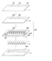
- FIG. 1 schematically shows an example of an ink jet head according to an embodiment of the present invention, disassembled for each component, and the ink jet head HD includes a first silicon substrate 1, a second silicon substrate 2, a piezoelectric element 3, and A reinforcing member 5 is provided.
- a plurality of ink discharge ports 101 are formed through the first silicon substrate 1.
- the second silicon substrate 2 is covered with the first silicon substrate 1 and bonded to form a pressure chamber groove 204 serving as a pressure chamber, an ink supply channel groove 203 serving as an ink supply path, and a common pressure chamber.
- a common pressure chamber groove 202 and an ink supply port 201 are formed.
- the first silicon substrate 1 and the second silicon substrate 2 are bonded so that the ink discharge port 101 of the first silicon substrate 1 and the pressure chamber groove 204 of the second silicon substrate 2 correspond one-to-one. Is done.
- the piezoelectric element 3 is bonded to a position corresponding to each pressure chamber 204 on the surface of the second silicon substrate 2 opposite to the surface to be bonded to the first silicon substrate 1.
- the piezoelectric element 3 is an actuator that is made of PZT (lead zirconate titanate) and ejects ink from the ink ejection port 101.
- the reinforcing member 5 is bonded to the surface of the second silicon substrate 2 opposite to the surface to which the first silicon substrate 1 is bonded.
- a chamber formed by the pressure chamber groove 204 and the first silicon substrate 1 is referred to as a pressure chamber 204, and a chamber formed by the ink supply channel groove 203 and the first silicon substrate 1 is referred to as a pressure chamber 204.
- a chamber formed by the common pressure chamber groove 202 and the first silicon substrate 1 is referred to as an ink supply path 203 and is referred to as a common pressure chamber 202.
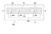
- FIG. 2 is a plan view of the inkjet head shown in FIG.
- FIG. 3 is an enlarged sectional view taken along line X in FIG.
- the reinforcing member 5, the second silicon substrate 2, and the first silicon substrate 1 are arranged in this order from the top, and the ink ejection surface 1a (lower surface) of the first silicon substrate 1 on which ink droplets are ejected. ) Is formed in a plane.
- Each pressure chamber 204 has an opening area larger than that of the ink discharge port 101 formed in the first silicon substrate 1, and from a bonding surface (pressure chamber forming surface) with the first silicon substrate 1. It is recessed at a predetermined depth.
- the piezoelectric elements 3 are individually bonded to the back side of each pressure chamber 204, that is, the side opposite to the bonding surface of the second silicon substrate 2 with the first silicon substrate 1.
- Each piezoelectric element is connected to drive pulse generating means (not shown) through electrodes (not shown) provided on both upper and lower surfaces.
- the piezoelectric element is deformed, and the bottom 25 of each pressure chamber 204 is vibrated by the electro-mechanical conversion action of this piezoelectric element 3,
- the pressure wave is generated in the ink in the pressure chamber 204 by changing the volume of the ink.
- the ink meniscus in the ink discharge port 101 vibrates and is ejected from the ink discharge port 101 to form ink droplets, which are ejected downward in the figure.
- each pressure chamber 204 functions as a diaphragm. For this reason, the depth of the recess when the pressure chamber 204 is dry-etched on the second silicon substrate 2 is adjusted so that the thickness of the bottom surface 25 of each pressure chamber 204 is preferably 1 to 20 ⁇ m. .
- the reinforcing member 5 has an opening 501 that opens a first region R ⁇ b> 1 including a region in which the pressure chambers 204 and the piezoelectric elements 3 are disposed, and a region in which partition walls separating the individual pressure chambers 204 are disposed. And is formed as a frame-shaped member that covers the second region R2 surrounding the first region R1.
- the reinforcing member 5 imparts rigidity to the second silicon substrate 2, and suppresses crosstalk by suppressing the entire second silicon substrate 2 from vibrating when the diaphragm is vibrated by the piezoelectric element 3.
- it is formed of a material having high rigidity such as aluminum, stainless steel or glass having a thickness of 200 to 500 ⁇ m, and is bonded to the lower surface of the second silicon substrate 2 using an adhesive.
- the reinforcing member 5 is molded from a plate material to a desired size by machining, and the opening 501 is also formed by machining.
- the first silicon substrate 1 is manufactured by using a silicon substrate having a thickness of about 150 ⁇ m to 500 ⁇ m as a base material, for example, using a known photolithography technique (resist coating, exposure, development), an etching technique, and the like. This is performed by a procedure of penetrating the ink discharge port 101.
- the hole diameter of the ink discharge port 101 is about ⁇ 1 ⁇ m to ⁇ 30 ⁇ m.
- the second silicon substrate 2 uses a silicon substrate having a thickness of about 150 ⁇ m to 500 ⁇ m as a base material.
- a known photolithography technique resist coating, exposure, By using development and etching techniques, etc.
- pressure chamber grooves 204 serving as a plurality of pressure chambers respectively communicating with the ink discharge ports 101 of the first silicon substrate 1 and a plurality of ink supply paths communicating with the pressure chambers are obtained.
- An ink supply path groove 203, a common pressure chamber groove 202 serving as a common pressure chamber communicating with the ink supply path, and an ink supply port 201 are formed.
- the pressure chamber groove 204 has a width of about 150 ⁇ m to 350 ⁇ m, a depth of about 50 ⁇ m to 200 ⁇ m, and an ink supply.
- the channel groove 203 has a width of about 50 ⁇ m to 150 ⁇ m, a depth of about 30 ⁇ m to 150 ⁇ m
- the common pressure chamber groove has a width of about 400 ⁇ m to 1000 ⁇ m, a depth of about 50 ⁇ m to 200 ⁇ m
- the ink supply port 201 is a through-hole with a diameter of about ⁇ 400 ⁇ m to 1500 ⁇ m. is there.
- the etching method for the silicon substrate is preferably a silicon (Si) anisotropic dry etching method capable of performing etching processing perpendicularly to the surface of the second silicon substrate.
- silicon (Si) anisotropic dry etching method Sangyo Tosho Co., Ltd. “Semiconductor dry etching technology” can be referred to.
- first silicon substrate 1 and the second silicon substrate 2 processed by the method described so far are bonded using an anodic bonding technique. This will be described below.
- FIG. 4 is a diagram showing a bonding process between the first silicon substrate 1 and the second silicon substrate 2, and FIG. 4A shows an ink discharge port (not shown) using the silicon substrate as a base material.
- the first silicon substrate 1 and the second silicon substrate 2 in which grooves such as the pressure chamber groove 204 are formed by the above-described processing.
- the first silicon substrate 1 and the second silicon substrate 2 are bonded by anodic bonding.
- silicon is used as a material constituting one of the substrates, and the other is silicon with a mobile ion, for example, a glass material containing sodium ions (Na + ).
- a material having a linear expansion coefficient relatively similar to (Si) (the linear expansion coefficient of silicon is about 4.2 ⁇ 10 ⁇ 6 / ° C.), for example, borosilicate glass is used. .
- borosilicate glass containing mobile ions hereinafter referred to as borosilicate glass
- Pyrex registered trademark
- Corning USA
- Tempax Float registered trademark
- Shot Japan Co., Ltd. have these linear expansion coefficients ⁇
- the linear expansion coefficients of Pyrex (registered trademark) and Tempax Float (registered trademark) are both about 3.2 ⁇ 10 ⁇ 6 / ° C. ⁇ Is more preferable from the viewpoint of.
- a silicon substrate is used instead of borosilicate glass as a base material. Then, a borosilicate glass film is formed on the bonding surface of the silicon substrate as the base material to form a borosilicate glass surface.
- the film thickness in this case may be a film thickness that can be strongly bonded by anodic bonding, and is 0.5 ⁇ m from the viewpoint of the density and uniformity of the film and the heating and applied voltage of the bonding surface required during anodic bonding described later.
- the range of ⁇ 3 ⁇ m is preferable, and the range of 1 ⁇ m to 2 ⁇ m is more preferable.
- the borosilicate glass film may be formed by any one of a vacuum deposition method, a radio frequency (RF) magnetron sputtering method, and an ion plating method, and the substrate temperature is easily formed at the time of film formation. It is preferable to heat so that it may become 250 degreeC or more.
- the upper limit of the temperature is not particularly defined, but is preferably about 400 ° C. from the viewpoint of a substrate mounting jig, a substrate temperature control device during film formation, and the like.
- the base materials of the first silicon substrate 1 and the second silicon substrate 2 are both silicon substrates for ease of fine processing. Therefore, one of the bonding surfaces of the first silicon substrate 1 and the second silicon substrate 2 needs to be the borosilicate glass surface described above.
- a borosilicate glass film is provided on the second silicon substrate 2 side, it is predicted that deformation due to the deposition of the film will occur in the already formed fine shape due to the film thickness that forms the surface of the borosilicate glass. Is done.
- the bottom 25 (vibration plate) of the pressure chamber 204 is thickened by this film, so that the structure of the pressure chamber 204 itself is strengthened and distortion due to the piezoelectric element 3 cannot be sufficiently generated. As a result, ink cannot be sufficiently discharged.
- the drive power of the piezoelectric element 3 must be increased.
- the surface side of the first silicon substrate 1 shown in FIG. 4B that covers the second silicon substrate is a borosilicate glass surface, and the first silicon substrate 1 is used as the substrate, and the second of the substrate is the second one.
- a relatively thick borosilicate glass thick film 110 in the range of 0.5 ⁇ m to 3 ⁇ m is provided on the surface side covering the silicon substrate.
- the polarity of the voltage applied when anodic bonding is performed is positive (+) on the silicon substrate side and negative (-) on the borosilicate glass substrate side. If it does in this way, an electric current will flow at the same time that a joining interface closely_contact
- the second silicon substrate 2 is applied with a positive (+) voltage
- the first silicon substrate 1 having the borosilicate glass thick film 110 is applied with a negative ( ⁇ ) voltage. It ’s fine.
- the high temperature state at the time of joining is in the range of 300 ° C. to 550 ° C.
- a constant temperature bath capable of maintaining such an atmospheric temperature or a simple method using a hot plate having good insulation with a built-in ceramic heater or the like. What is necessary is just to heat the junction part of the 1st silicon substrate 1 and the 2nd silicon substrate 2.
- the electric field strength of the DC voltage applied between the first silicon substrate 1 and the second silicon substrate 2 by the DC high voltage power source 4 is preferably in the range of 30 kV / mm to 200 kV / mm.
- the applied voltage range is 15 to 100 V, and if it is 3 ⁇ m, it is 90 to 600 V.
- the bonding surfaces are all anodic bonded so that no adhesive is present at all the bonding portions, the entire ink jet head is given rigidity, and the vibration plate is vibrated by the piezoelectric element 3.
- the piezoelectric element 3 is bonded to the combined body A of the first silicon substrate 1 and the second silicon substrate 2 bonded by anodic bonding as described above, and an ink jet head is completed.
- the inkjet head HD is designed so that the drive frequency and fluid resonance frequency of the inkjet head are not included in the frequency range within the half width with respect to the structural resonance frequency of the inkjet head.
- the structural resonance frequency of the inkjet head can be obtained by numerical calculation or experiment.
- a drive voltage waveform obtained by sweeping the drive frequency is input to a piezoelectric element in one pressure chamber, and ink is ejected. From the deformation amount of the head at that time, for example, the deformation amount of the ink ejection surface It can be calculated. When the drive frequency versus the deformation amount is plotted, the frequency at which the deformation amount reaches the maximum value becomes the resonance point, which is the structural resonance frequency of the inkjet head.
- analysis can be performed using general-purpose numerical analysis software, or if it can be approximated to a simple model, it can be easily calculated without using software.
- the structural resonance frequency of the inkjet head HD can be changed by adjusting the overall thickness of the inkjet head HD, the area of the opening 501 of the reinforcing member 5, and the like. For example, the structural resonance frequency is lowered because the rigidity is lowered by reducing the overall thickness or increasing the area of the opening 501 of the reinforcing member 5.
- the thickness of at least one of the first silicon substrate 1, the second silicon substrate 2, and the reinforcing member 5 may be reduced, or the reinforcing member 5 may be eliminated.
- the drive frequency of the inkjet head can be changed by adjusting the drive frequency of the piezoelectric element 3.
- the fluid resonance frequency of the inkjet head is a resonance frequency of a plurality of fluid vibration modes generated when a pressure wave is excited in ink (fluid) in the pressure chamber 204 when the piezoelectric element 3 is driven.
- One of them is the resonance frequency of the natural vibration of the pressure chamber, conventionally called Helmholtz vibration.
- the other is the resonance frequency of the natural vibration (hereinafter referred to as the meniscus natural vibration) caused by the meniscus free surface in the ink discharge port.
- a plurality of vibration modes and resonance points thereof that is, the resonance frequency f1 of the natural vibration of the meniscus in the nozzle and the resonance frequency f2 of the natural vibration of the pressure chamber can be obtained by numerical calculation or experiment.
- analysis can be performed using general-purpose numerical analysis software, or if it can be approximated to a simple model, it can be easily calculated without using software.
- L is an inertance component [kg / m 4 ]
- La is an inertance component in the piezoelectric element
- Ln is an inertance component in the ink discharge port
- Li is an inertance component in the ink supply path
- Lc is in the pressure chamber.
- R is a resistance component [N ⁇ s / m 5 ]
- Ra is a resistance component in the piezoelectric element
- Rn is a resistance component in the ink ejection port
- Ri is a resistance component in the ink supply path
- Rc is a resistance component in the pressure chamber. is there.
- C is a capacitive component [m 5 / N]
- Ca is a capacitive component in the piezoelectric element
- Cn is a capacitive component in the ink ejection port
- Ci is a capacitive component in the ink supply path
- Cc is a capacitive component in the pressure chamber.
- the inertance component L in each part is given by equation (1), where S [m 2 ] is the cross-sectional area of the flow path, l [m] is the flow path length, and ⁇ [kg / m 3 ] is the ink density. It is done.
- ⁇ is a shape factor determined by the cross-sectional shape of the flow path, and is about 1.3 when the cross-section is circular or rectangular.
- the resistance component R in each part is given by the equation (2) when the ink viscosity is ⁇ [Pa ⁇ s] and the diameter is d [m] when the flow path cross section is circular.
- Cc and Ca which are terms related to compression inside the fluid, are V [m 3 ] for the pressure chamber volume, ⁇ [kg / m 3 ] for the ink density, and c [m / s] for the sound velocity of the ink. It is given by equation (3).
- Cn which is a term related to the fluid free surface, is given by equation (4), where the surface tension ⁇ [N / m] of the ink and the diameter of the ink discharge port are d [m].
- the elements Ci, Ra, and La that have little influence on the characteristics are set to approximately zero, and the remaining elements are synthesized, so that the vibration mode is separated into two.
- the first vibration mode is mode 1, the resonance point is f1, the second vibration mode is mode 2, and the resonance point is f2.
- Vibration mode 1 is the natural vibration of the meniscus that occurs on the surface of the meniscus.
- the vibration mode 2 is a natural vibration of the pressure chamber caused by pressure fluctuation in the pressure chamber, and the meniscus is raised when this is transmitted to the ink discharge port. This is conventionally called Helmholtz vibration.
- the resonance frequency f1 of the meniscus natural vibration is expressed by the following equation (5).
- the resonance frequency f2 of the natural vibration of the pressure chamber is expressed by the following equation (6).
- the parameters governing f1 and f2 are only the inertance component and the capacitance component of each part. That is, f1 and f2 are determined by the combination of the inertance component and the capacitance component of each part.
- the resonance frequency of the fluid vibration mode of the inkjet head HD can be adjusted by adjusting the size and shape of the ink discharge port 101, the pressure chamber 204, and the ink supply path 203 of the inkjet head HD.
- the inkjet head HD is designed so that the drive frequency and fluid resonance frequency of the inkjet head are not included in the frequency range within the half width with respect to the structural resonance frequency of the inkjet head. For this reason, the drive frequency of the inkjet head and the fluid resonance frequency can be separated from the frequency region within the half width with respect to the structural resonance frequency of the inkjet head, and by suppressing the structural resonance of the inkjet head, The vibration of the head and the occurrence of crosstalk that occur during driving can be suppressed, unstable ejection states such as crosstalk are unlikely to occur, and the ejection characteristics are stabilized.
- FIG. 5 is a plan view of another example of the inkjet head HD according to the embodiment of the present invention.
- the reinforcing member 5 has an opening 501 that opens the first region R1 including the region of the common pressure chamber 202. That is, a partition wall such as a region where the pressure chamber 204 and the piezoelectric element 3 are disposed, a region where the ink supply path 203 is disposed, a region where the common pressure chamber 202 is disposed, and a partition partitioning the individual pressure chambers 204 are disposed.
- the reinforcing member 5 is formed as a frame member that has an opening 501 that opens the first region R1 including the region and covers the second region R2 that surrounds the first region R1.
- the inkjet head HD of this example is designed so that the drive frequency and fluid resonance frequency of the inkjet head are not included in the frequency range within the half-value width with respect to the structural resonance frequency of the inkjet head. For this reason, by suppressing the structural resonance of the inkjet head, it is possible to suppress the vibration of the head and the occurrence of crosstalk during driving, and it is difficult for unstable discharge states such as crosstalk to occur, and the discharge characteristics Is stabilized.
- the area where the common pressure chamber 202 is arranged is also opened.
- flow path crosstalk is generated in which the pressure wave is transmitted to the non-driven pressure chamber via the common pressure chamber 202, but the area where the common pressure chamber is disposed is opened as in this example.
- the pressure wave in the common pressure chamber can be absorbed by the vibration of the wall forming the common pressure chamber, and the flow path crosstalk can be suppressed.
- FIG. 6 is a diagram schematically showing still another example of the ink jet head HD according to the embodiment of the present invention.
- a glass substrate 6 is provided between the first silicon substrate 1 and the second silicon substrate 2.
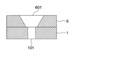
- the glass substrate 6 has an ink flow path hole 601 at a position corresponding to the ink discharge port 101.
- the ink flow path hole 601 has a larger diameter than the ink discharge port 101 of the first silicon substrate 1 as shown in FIG.
- the glass substrate 6 is bonded to the second silicon substrate 2 and the first silicon substrate 1 by anodic bonding. Therefore, borosilicate glass is preferable as the material of the glass substrate 6.
- the inkjet head HD of this example is designed so that the drive frequency and fluid resonance frequency of the inkjet head are not included in the frequency range within the half-value width with respect to the structural resonance frequency of the inkjet head. For this reason, by suppressing the structural resonance of the inkjet head, it is possible to suppress the vibration of the head and the occurrence of crosstalk during driving, and it is difficult for unstable discharge states such as crosstalk to occur, and the discharge characteristics Is stabilized.
- the bonding surfaces are all anodic bonded so that no adhesive is present at all the bonding portions, the entire ink jet head is given rigidity, and the vibration plate is vibrated by the piezoelectric element 3.
- ink discharge ports 101 and the pressure chambers 204 that require a high degree of miniaturization can be processed and formed on the silicon substrates 1 and 2, a fine and high-density pattern can be formed by using a semiconductor integrated circuit manufacturing technique. Is possible.
- the glass substrate 6 is simply formed with a simple through hole, and the processing operation during dry etching is extremely simple.
- FIGS. 8 and 9 show still another example of the ink jet head according to the embodiment of the present invention, in which the pressure chambers, piezoelectric elements, and ink discharge ports are arranged in two rows.
- the piezoelectric element group 3A, the piezoelectric element group 3B, and the pressure chamber groups 204A and 204B are arranged in two upper and lower rows, and although not shown, ink discharge ports corresponding to these are arranged.
- a common pressure chamber 202A corresponding to the upper pressure chamber group 204A is disposed above the pressure chamber group 204a, and a corresponding common pressure chamber 202B is disposed below the lower pressure chamber group 204B.
- the reinforcing member 5 is formed as a frame-shaped member that opens the region R1 including the pressure chamber groups 204A and 204B and the common pressure chamber groups 202A and 202B and covers the region R2 surrounding the region R1.
- the arrangement of the pressure chamber group, the piezoelectric element group, and the ink discharge port group is the same as that in FIG. 8, but the shape of the reinforcing member 5 is different from that in FIG.
- the region R11 including 3A, the lower pressure chamber group 204B, the region R12 including the piezoelectric element group 3B, the region R13 including the upper common pressure chamber 202A, and the region R14 including the lower common pressure chamber 202B are opened.
- the reinforcing member 5 is formed as a frame-like member that covers the region surrounding the region.
- a region R22 between the lower pressure chamber group 204B and a region R23 between the lower pressure chamber group 204B and the lower common pressure chamber 202B is a region covered with the reinforcing member 5.
- the inkjet head HD of this example is designed so that the drive frequency and fluid resonance frequency of the inkjet head are not included in the frequency range within the half-value width with respect to the structural resonance frequency of the inkjet head. For this reason, by suppressing the structural resonance of the inkjet head, it is possible to suppress the vibration of the head and the occurrence of crosstalk during driving, and it is difficult for unstable discharge states such as crosstalk to occur, and the discharge characteristics Is stabilized.
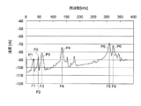
- the vertical axis in FIGS. 10 and 11 represents the speed (differential displacement value) when the amount of deformation of the head measured with a laser Doppler meter when driving one pressure chamber by sine wave input, and the horizontal axis represents the drive. Indicates the frequency.
- the numerical value of the velocity on the vertical axis corresponds to the deformation amount of the head, and the larger the numerical value, the larger the deformation amount of the head, that is, the amplitude of vibration.
- FIG. 10 shows the amount of head deformation when a reinforcing member whose thickness is adjusted is provided
- FIG. 11 shows the amount of head deformation when a reinforcing member whose thickness is not adjusted is provided.
- each symbol means the following.
- any one of the resonance frequencies (peak values) of each resonance spectrum matches or is close to the drive frequency or fluid resonance frequency of the inkjet head, structural resonance of the head occurs, which adversely affects ejection stability. Effect.
- the driving frequency of the inkjet head and the fluid resonance frequency are included in a frequency range within a half-value width with respect to the structural resonance frequency of the inkjet head. It is necessary to set not to.
- Such setting is performed, for example, by adjusting the thickness of the reinforcing member 5 in FIG. If the adjustment is made on the ink jet head main body side, the ejection characteristics may change. Therefore, it is advantageous to adjust the structural resonance frequency by the reinforcing member 5.
- fluid resonance frequencies f1 and f2 are determined for the flow path shape and ink physical properties of the head.
- the fluid resonance point of this head is that the resonance frequency f2 of the natural vibration of the pressure chamber is 98 kHz and the resonance frequency f1 of the natural vibration of the meniscus is 335 kHz, and droplets having different diameters can be formed in each mode. .
- FIG. 11 shows the case where the thickness of the reinforcing member 5 is not adjusted, and the first to sixth resonance spectra are separated from 98 kHz, which is the resonance frequency f2 of the natural vibration of the pressure chamber.
- This f2 is not included in any of the frequency regions ⁇ F1 to ⁇ F6 within the half-value widths of the first to sixth resonance spectra.
- the inkjet head is ejected at a drive frequency of less than 25 kHz, and the drive frequency is not included in the frequency region ⁇ F within the full width at half maximum with respect to all the resonance frequencies F, and the ejection stability is good. It was confirmed that.
- the driving frequency of the inkjet head and f1 or f2 were examined. Is included in the frequency region ⁇ F within the half width with respect to any of the resonance frequencies F, the ejection stability is poor, and the drive frequency of the inkjet head or f1 or f2 is within the frequency region ⁇ F within the half width with respect to all the resonance frequencies F. When it was not included, it was confirmed that the ejection stability was good.
- the drive frequency of the ink jet head or the fluid resonance frequency and the structural resonance frequency coincide with each other or interfere with each other, the ejection becomes unstable, or an unintended change occurs with respect to the change of the discharge condition.
- the interference can be prevented by designing the reinforcement in consideration of the drive frequency and resonance frequency of the inkjet head.
- the ink jet head HD suppresses the occurrence of crosstalk due to resonance of the ink jet head when ink is ejected, the ejection characteristics are stabilized.
Landscapes
- Particle Formation And Scattering Control In Inkjet Printers (AREA)
Abstract
駆動時に発生するヘッドの振動やクロストークの発生を抑制し得るインクジェットヘッドを提供することを目的とし、複数のインク吐出口と、各インク吐出口に連通する複数の圧力室と、各圧力室の容積を変化させることによりインクに圧力を発生させる圧電素子と、を備え、インクジェットヘッドの駆動周波数及び流体的な共振周波数が、前記インクジェットヘッドの構造的な共振周波数に対する半値幅内の周波数領域に含まれないことを特徴とするインクジェットヘッド。
Description
本発明は、インクジェットヘッドに関する。
圧電素子を利用した方式のインクジェットヘッドには、縦振動モードを利用したものとたわみ振動モードを利用したものとがあるが、後者はヘッド全体を薄くすることが可能であり、ヘッドの製造工程に薄膜プロセスを多く取り入れることができ、集積化に向いているという特長がある。
しかるに、後者のインクジェットヘッドにおいては、記録動作時に、駆動している圧力室以外でも変形が起こるという問題があり、特に、多数のインク吐出口を同時駆動するときに、クロストークなどが顕著になる。
このために、
・圧力室の変位ロスが発生し、駆動効率が低下する
・駆動していない隣接圧力室の体積も変化するクロストークが起こる
・駆動するインク吐出口数によってインク吐出特性が変化する
等の望ましくない現象が起こる。
・圧力室の変位ロスが発生し、駆動効率が低下する
・駆動していない隣接圧力室の体積も変化するクロストークが起こる
・駆動するインク吐出口数によってインク吐出特性が変化する
等の望ましくない現象が起こる。
このような問題に対する対策として、特許文献1では、圧力室を形成するなどのヘッド基板の処理時に、補強部材を形成し、圧力室を隔てる隔壁に補強部材を設けることが提案されている。
特許文献1のように、補強部材を取り付けて上記隔壁の剛性を向上させることにより、クロストークを低減することは可能である。
しかしながら、上記従来のヘッドでは、圧電素子を駆動してインクを吐出させる際、インクジェッドヘッドの構造的な共振周波数が、インクジェットヘッドの駆動周波数(圧電素子の駆動周波数)と一致または近接すると、インクジェッドヘッド全体が共振し、所謂クロストークが発生し不安定な吐出状態になるという問題がある。
また、圧電素子を駆動し、圧力室に体積変化を生じさせると、圧力室内に圧力波が発生する。この圧力波によってインク吐出口内のインクメニスカスが振動し、インク吐出口から排出されることでインク滴が形成される。この際、圧力室内のインク(流体)に圧力波が励起され、複数の流体的な共振が生じる。そのうちの1つは、従来よりヘルムホルツ振動と呼ばれている圧力室の固有振動である。その他には、インク吐出口内のメニスカス自由表面に起因する固有振動である。インクジェッドヘッドの構造的な共振周波数が、この流体的な共振周波数と一致または近接すると、インクジェッドヘッド全体が共振し、所謂クロストークが発生し不安定な吐出状態になるという問題がある。
特許文献1では、補強部材を取り付けて上記隔壁の剛性を向上させることにしか注目しておらず、液滴を吐出させる際のインクジェットヘッドの共振によるクロストークの発生について考慮されていない。
本発明はこのような事情に鑑みてなされたもので、駆動時に発生するヘッドの振動やクロストークの発生を抑制し得るインクジェットヘッドを提供することを目的とする。
前記目的は、下記の発明により達成される。
1.複数のインク吐出口と、各インク吐出口に連通する複数の圧力室と、各圧力室の容積を変化させることによりインクに圧力を発生させる圧電素子と、を備え、インクジェットヘッドの駆動周波数及び流体的な共振周波数が、前記インクジェットヘッドの構造的な共振周波数に対する半値幅内の周波数領域に含まれないことを特徴とするインクジェットヘッド。
2.複数の前記インク吐出口が貫通形成された第1のシリコン基板と、
一方の面に前記インク吐出口にそれぞれ対応する複数の前記圧力室が溝加工されると共に、他方の面に該圧力室内の容積を変化させるための前記圧電素子がそれぞれ設けられ、
前記一方の面側に設けられた該圧力室の形成面が前記第1のシリコン基板の一方の面に面するように接合された第2のシリコン基板と、を有し、
前記圧電素子の駆動によって前記圧力室内のインクを前記インク吐出口から吐出させることを特徴とする前記1に記載のインクジェットヘッド。
一方の面に前記インク吐出口にそれぞれ対応する複数の前記圧力室が溝加工されると共に、他方の面に該圧力室内の容積を変化させるための前記圧電素子がそれぞれ設けられ、
前記一方の面側に設けられた該圧力室の形成面が前記第1のシリコン基板の一方の面に面するように接合された第2のシリコン基板と、を有し、
前記圧電素子の駆動によって前記圧力室内のインクを前記インク吐出口から吐出させることを特徴とする前記1に記載のインクジェットヘッド。
3.複数の前記インク吐出口が貫通形成された第1のシリコン基板と、
前記第1のシリコン基板の一方の面に接合され、前記インク吐出口にそれぞれ対応する複数のインク流路孔が貫通形成されたガラス基板と、
一方の面に前記インク流路孔にそれぞれ対応する複数の前記圧力室が溝加工されると共に、他方の面に該圧力室内の容積を変化させるための前記圧電素子がそれぞれ設けられ、
前記一方の面側に設けられた該圧力室の形成面が前記ガラス基板に対して前記第1のシリコン基板とは反対面に面するように接合された第2のシリコン基板と、を有し、
前記圧電素子の駆動によって前記圧力室内のインクを前記インク吐出口から吐出させることを特徴とする前記1に記載のインクジェットヘッド。
前記第1のシリコン基板の一方の面に接合され、前記インク吐出口にそれぞれ対応する複数のインク流路孔が貫通形成されたガラス基板と、
一方の面に前記インク流路孔にそれぞれ対応する複数の前記圧力室が溝加工されると共に、他方の面に該圧力室内の容積を変化させるための前記圧電素子がそれぞれ設けられ、
前記一方の面側に設けられた該圧力室の形成面が前記ガラス基板に対して前記第1のシリコン基板とは反対面に面するように接合された第2のシリコン基板と、を有し、
前記圧電素子の駆動によって前記圧力室内のインクを前記インク吐出口から吐出させることを特徴とする前記1に記載のインクジェットヘッド。
4.前記第1のシリコン基板、前記ガラス基板、前記第2のシリコン基板の接合面がいずれも陽極接合されていることを特徴とする前記3に記載のインクジェットヘッド。
5.前記第2のシリコン基板における前記圧力室の形成面の反対面に、該第2のシリコン基板に剛性を付与するための補強部材が接合されていることを特徴とする前記2~4のいずれかに記載のインクジェットヘッド。
本発明によれば、インクジェットヘッドの駆動周波数及流体的な共振周波数が、前記インクジェットヘッドの構造的な共振周波数に対する半値幅内の周波数領域に含まれないようにすることにより、インクジェットヘッドの構造的な共振を抑制することで、駆動時に発生するヘッドの振動やクロストークの発生を抑制し得るインクジェットヘッドを提供することができる。
以下、図示の実施の形態により本発明を説明するが、本発明は該実施の形態に限られない。
図1は本発明の実施の形態に係るインクジェットヘッドの一例を構成要素毎に分解して模式的に示し、インクジェットヘッドHDは第1のシリコン基板1、第2のシリコン基板2、圧電素子3及び補強部材5を有する。
第1のシリコン基板1には、複数のインク吐出口101が貫通形成されている。
第2のシリコン基板2には、これに第1のシリコン基板1を被せて接合することで、圧力室となる圧力室溝204、インク供給路となるインク供給路溝203、共通圧力室となる共通圧力室溝202、及びインク供給口201が形成されている。
そして、第1のシリコン基板1のインク吐出口101と第2のシリコン基板2の圧力室溝204とが一対一で対応するように第1のシリコン基板1と第2のシリコン基板2とが接合される。
更に、第2のシリコン基板2の第1のシリコン基板1と接合する面と反対側の面の各圧力室204に対応した位置に圧電素子3が接着される。圧電素子3はPZT(チタン酸ジルコン酸鉛)からなり、インクをインク吐出口101から吐出させるアクチュエータである。
更に、第2のシリコン基板2の第1のシリコン基板1が接合された面と反対側の面に補強部材5が接着される。
なお、以下の説明において、圧力室溝204と第1のシリコン基板1とにより形成された部屋を圧力室204と言い、インク供給路溝203と第1のシリコン基板1とにより形成された部屋をインク供給路203と言い、共通圧力室溝202と第1のシリコン基板1とにより形成された部屋を共通圧力室202と言う。
図2は図1に示すインクジェットヘッドの平面図である。図3は図2における線Xに沿った拡大断面図である。
図3に示すように、上から補強部材5、第2のシリコン基板2、第1のシリコン基板1の順に配置され、インク滴が吐出される第1のシリコン基板1のインク吐出面1a(下面)は平面に形成される。
各圧力室204は、第1のシリコン基板1に形成されているインク吐出口101よりも大きな開口面積を有しており、第1のシリコン基板1との接合面(圧力室の形成面)から所定の深さで凹設されている。各圧力室204の背面側、すなわち第2のシリコン基板2における第1のシリコン基板1との接合面の反対面側には、圧電素子3が個別に接着されている。
また、各圧電素子は、上下両面に設けられた電極(不図示)を経て駆動パルス発生手段(不図示)に接続されている。駆動パルス発生手段より、これらの電極間に電圧が印加されると、圧電素子が変形し、この圧電素子3の電気-機械変換作用によって各圧力室204の底面25を振動させ、圧力室204内の容積を変化させることにより、圧力室204内のインクに圧力波が発生する。この圧力波によってインク吐出口101内のインクメニスカスが振動し、インク吐出口101から排出されることでインク滴が形成され、図示下方向に吐出される。
このように、各圧力室204の底面25は振動板として機能する。このため、各圧力室204の底面25の厚みは、好ましくは1~20μmとなるように、第2のシリコン基板2に各圧力室204をドライエッチングする際の凹設深さが調節されている。
図2に示すように、補強部材5は圧力室204及び圧電素子3が配置された領域、並びに個々の圧力室204を隔てる隔壁が配置された領域を包含する第1領域R1を開放する開口501を有し、第1領域R1を囲む第2領域R2を覆う枠状の部材として形成される。
補強部材5は、第2のシリコン基板2に剛性を付与し、振動板が圧電素子3によって振動する際に第2のシリコン基板2全体が振動することを抑制することで、クロストークを抑制する効果を高めるためのものであり、例えば、厚さ200~500μmを有するアルミ、ステンレス、ガラス等高い剛性を有する材料によって形成され、第2のシリコン基板2の下面に接着剤を用いて接着されている。また、補強部材5は板材料から機械加工により所望のサイズに成型されるとともに、開口501も機械加工により形成される。
次に、インクジェットヘッドHDの作成について説明する。
第1のシリコン基板1の作製方法は、基材として厚みが150μm~500μm程度のシリコン基板を用いて、例えば、公知のフォトリソグラフィー技術(レジスト塗布、露光、現像)とエッチング技術等を用いることでインク吐出口101を貫通形成するという手順により行われる。このインク吐出口101の穴径は、概ねφ1μm~φ30μm程度である。
第2のシリコン基板2は、第1のシリコン基板1の作製方法と同様に、基材として厚みが150μm~500μm程度のシリコン基板を用いて、例えば、公知のフォトリソグラフィー技術(レジスト塗布、露光、現像)とエッチング技術等を用いることで、第1のシリコン基板1のインク吐出口101にそれぞれ連通する複数の圧力室となる圧力室溝204、圧力室にそれぞれ連通する複数のインク供給路となるインク供給路溝203、及びインク供給路に連通する共通圧力室となる共通圧力室溝202、並びにインク供給口201とを形成する。
ここで形成する溝の大きさは、適宜に決められるが、本実施の形態の一例であるインクジェットヘッドでは、例えば、圧力室溝204は幅150μm~350μm程度、深さ50μm~200μm程度、インク供給路溝203は幅50μm~150μm程度、深さ30μm~150μm程度、共通圧力室溝は幅400μm~1000μm程度、深さ50μm~200μm程度、インク供給口201は直径φ400μm~1500μm程度の貫通した穴である。
シリコン基板に対するエッチング加工方法は、第2のシリコン基板の面に対して垂直にエッチング加工ができるシリコン(Si)異方性ドライエッチング法が好ましい。シリコン(Si)異方性ドライエッチング法に関しては、産業図書株式会社「半導体ドライエッチング技術」等を参照することが出来る。
次に、これまで説明した方法で加工されている第1のシリコン基板1と第2のシリコン基板2とを陽極接合技術を用いて接合する。以下に、これに関して説明する。
図4は、第1のシリコン基板1と第2のシリコン基板2との接合工程を示す図であり、図4(a)は、シリコン基板を基材として、インク吐出口(図示してない。)が加工された第1のシリコン基板1及び圧力室溝204等の溝が前記に説明した加工により形成された第2のシリコン基板2を示している。
第1のシリコン基板1と第2のシリコン基板2とは陽極接合により結合される。陽極接合技術を用いて2つの基材を接合する場合、基材の一方を構成する材料としてシリコンを用い、他方を可動イオン、例えば代表的にはナトリウムイオン(Na+)を含むガラス材でシリコン(Si)と比較的類似した線膨張係数(シリコンの線膨張係数は、4.2×10⁻⁶/℃程度である。)を有するものを用いることが好ましく、例えば、硼珪酸ガラスが用いられる。
ここで、可動イオンを含む硼珪酸ガラス(以下、硼珪酸ガラスと称する。)としては、パイレックス(登録商標)、コーニング社(米国)またはテンパックス フロート(登録商標)、日本以外はBOROFLOAT(登録商標)、ショット日本(株)がこれらの線膨張係数{パイレックス(登録商標)及びテンパックス フロート(登録商標)の線膨張係数は共に3.2×10⁻⁶/℃程度である。}の観点からより好ましい。
また、硼珪酸ガラスよりシリコンの方が微細な加工が容易であることから、基材として硼珪酸ガラスではなく、シリコン基板を用いるようにする。そして、基材であるシリコン基板の接合面に硼珪酸ガラスを成膜して硼珪酸ガラス面とする。この場合の膜厚は、陽極接合にて強固に接合される膜厚であれば良く、膜の密度や均一性及び後述する陽極接合時に必要な接合面の加熱や印加電圧の観点から0.5μm~3μmの範囲が好ましく、更には1μm~2μmの範囲がより好ましい。
更に、この場合硼珪酸ガラスの成膜方法は、真空蒸着法や高周波(RF)マグネトロンスパッタ法、イオンプレーティング法のいずれでも良く、また成膜時に基板の温度を緻密な膜が形成しやすいように250℃以上となるように加熱することが好ましい。この温度の上限は特に定めないが、基板の取り付け治具や成膜時の基板の温度制御装置等の観点から400℃程度が好ましい。
本実施の形態の一例であるインクジェットヘッドでは、微細な加工の容易さから第1のシリコン基板1と第2のシリコン基板2の基材はいずれもシリコン基板としている。よって、第1のシリコン基板1と第2のシリコン基板2との接合面のいずれか一方を上記で示した硼珪酸ガラスの面にする必要がある。
仮に、第2のシリコン基板2側に硼珪酸ガラス膜を設けた場合、その硼珪酸ガラスの面を成す膜厚により、既に形成されている微細形状に膜の堆積による変形が発生することが予測される。また、この膜により圧力室204の底25(振動板)が厚くなることで圧力室204自体の構造が強固になり圧電素子3による歪みが十分発生できなくなり、その結果、インクの吐出が十分できない又は圧電素子3の駆動電力を大きくしなければならいといった問題が発生する恐れがある。
従って、図4(b)に示す第1のシリコン基板1の第2のシリコン基板に被さる面側を硼珪酸ガラスの面としており、第1のシリコン基板1を基板とし、この基板の第2のシリコン基板に被さる面側に0.5μm~3μmの範囲の比較的厚い膜厚の硼珪酸ガラス厚膜110を設ける。
次に、上記で説明した硼珪酸ガラスが所定の膜厚で成膜された第1のシリコン基板1と第2のシリコン基板2とを、図4(c)で示す通りに、適切な位置関係にして重ね合わせて固定し、接合部の温度を高温状態にして、直流高圧電源4を用いて電圧を印加して陽極接合する。以下に、第1のシリコン基板1と第2のシリコン基板2を陽極接合することに関して具体的に説明する。
陽極接合を行う場合に印加する電圧の極性は、シリコンの基材側をプラス(+)、硼珪酸ガラスの基材側をマイナス(-)とする。このようにすると、静電引力によって接合界面が密着すると同時に電流が流れ、両基板が強固に陽極接合される。
本実施の形態の一例であるインクジェットヘッドにおいては、第2のシリコン基板2はプラス(+)、硼珪酸ガラス厚膜110を有する第1のシリコン基板1はマイナス(-)とする電圧を印加すれば良い。
接合時の高温状態とは、300℃~550℃の範囲であって、このような雰囲気温度を維持できる恒温漕や簡便な方法ではセラミックヒーター等を内蔵する絶縁性の良いホットプレート等を用いて第1のシリコン基板1と第2のシリコン基板2との接合部を加熱すれば良い。
上記の温度範囲を超えて接合を行う場合、接合ができない又は接合が十分でないといった不都合が生じやすくなる。例えば、550℃以上では、印加電圧にもよるが、可動イオンが一気に流れ出して、硼珪酸ガラス膜が白濁したり膜密度が粗くなったりといった劣化が生じ、結果的に強固な接合ができない場合がある。また、300℃以下では、可動イオンが移動しにくい状態であり、これを移動しやすくするためには、印加電圧を大きくすることが必要である。印加電圧を大きくする結果、第1のシリコン基板1と第2のシリコン基板2との間での短絡が発生し、結果として陽極接合が十分できない場合がある。
また、直流高圧電源4にて第1のシリコン基板1と第2のシリコン基板2との間に印加する直流電圧の電界強度は、30kV/mm~200kV/mmの範囲が好ましい。例えば、硼珪酸ガラスの膜厚が0.5μmであれば、印加電圧の範囲は、15V~100V、また、3μmであれば90V~600Vとなる。
通常、1kVを超える電圧を使用する場合、電圧を発生する直流高圧電源4の容量や電圧印加に関連する附帯装置の絶縁耐圧を確保することが必要となるなどから、直流高圧電源4を含めた装置が高価かつ煩雑になる。従って、適当な膜厚を設定することで陽極接合時に印加する電圧を扱いやすい1kV未満とするのが好ましい。
本例では、これら各接合面はいずれも陽極接合することによって、全ての接合部位に接着剤が介在せず、インクジェットヘッド全体に剛性を付与し、振動板が圧電素子3によって振動する際に第2のシリコン基板2からインクジェットヘッド全体が振動することを抑制することで、クロストークを抑制する効果を高めることができる。
このように陽極接合により接合された第1のシリコン基板1及び第2のシリコン基板2の結合体Aに圧電素子3が接着され、インクジェットヘッドができあがる。
上記インクジェットヘッドHDは、インクジェットヘッドの駆動周波数及び流体的な共振周波数が、インクジェットヘッドの構造的な共振周波数に対する半値幅内の周波数領域に含まれないように設計されている。
インクジェットヘッドの構造的な共振周波数は、数値計算または実験により求めることができる。
実験により求める場合は、例えば、1つの圧力室の圧電素子に駆動周波数をスイープさせた駆動電圧波形を入力してインクを吐出させ、そのときのヘッドの変形量、例えばインク吐出面の変形量から算出できる。駆動周波数対変形量をプロットしたときに、変形量が極大値をとる周波数が共振点となり、インクジェットヘッドの構造的な共振周波数となる。
数値計算の場合には、汎用の数値解析ソフトで解析を行うか、簡単なモデルに近似できる場合はソフトを用いずに容易に計算できる。
インクジェットヘッドHDの構造的な共振周波数は、上記インクジェットヘッドHDの全体の厚みや補強部材5の開口501の面積等を調整することにより変更できる。例えば、全体の厚みを薄くするか、あるいは補強部材5の開口501の面積を大きくすることで剛性が低下するので構造的な共振周波数は低くなる。インクジェットヘッドHDの全体の厚みを薄くするには、第1のシリコン基板1、第2のシリコン基板2及び補強部材5の少なくとも1つの厚みを薄くするか、あるいは補強部材5をなくせばよい。
また、インクジェットヘッドの駆動周波数は、圧電素子3の駆動周波数を調整することにより変更できる。
インクジェットヘッドの流体的な共振周波数は、圧電素子3を駆動する際、圧力室204内のインク(流体)に圧力波が励起されることにより生じる複数の流体振動モードの共振周波数である。そのうちの1つは、従来よりヘルムホルツ振動と呼ばれている圧力室の固有振動の共振周波数である。その他には、インク吐出口内のメニスカス自由表面に起因する固有振動(以下、メニスカスの固有振動と称する。)の共振周波数である。
複数の振動モード及びその共振点、即ち、本発明におけるノズル内のメニスカスの固有振動の共振周波数f1、圧力室の固有振動の共振周波数f2は、数値計算または実験により求めることができる。
実験により求める場合は、圧電素子に正弦波の駆動電圧波形をスイープさせて入力し、そのときのメニスカス隆起量から算出できる。正弦波の周波数対隆起量(もしくは流量)をプロットしたときに、隆起量が極大値をとる周波数が共振点となり、固有振動の共振周波数となる。
数値計算の場合には、汎用の数値解析ソフトで解析を行うか、簡単なモデルに近似できる場合はソフトを用いずに容易に計算できる。
ここで、等価回路法を用いた計算方法を説明する。
以下の説明において、記号Lはイナータンス成分〔kg/m4〕であり、Laは圧電素子におけるイナータンス成分、Lnはインク吐出口におけるイナータンス成分、Liはインク供給路におけるイナータンス成分、Lcは圧力室におけるイナータンス成分である。記号Rは抵抗成分〔N・s/m5〕であり、Raは圧電素子における抵抗成分、Rnはインク吐出口における抵抗成分、Riはインク供給路における抵抗成分、Rcは圧力室における抵抗成分である。記号Cは容量成分〔m5/N〕であり、Caは圧電素子における容量成分、Cnはインク吐出口における容量成分、Ciはインク供給路における容量成分、Ccは圧力室における容量成分である。
ここで、各部におけるイナータンス成分Lは、流路断面積をS[m2]、流路長さをl[m]、インク密度をρ[kg/m3]とすると、式(1)で与えられる。ここで、αは、流路の断面形状により決まる形状係数で、断面が円形または長方形の場合は約1.3になる。

また、各部における抵抗成分Rは、流路断面が円形の場合は、インク粘度をη[Pa・s]、直径をd[m]とすると、式(2)で与えられる。

そして、各部における容量成分Cは以下のようになる。
流体内部の圧縮に関わる項であるCc、Caは、圧力室の容積をV[m3]、インク密度をρ[kg/m3]、インクの音速度をc[m/s]とすると、式(3)で与えられる。

流体自由表面に関わる項であるCnは、インクの表面張力σ[N/m]、インク吐出口の直径をd[m]とすると、式(4)で与えられる。

通常の設計範囲においては、特性にほとんど影響を及ぼさない要素Ci、Ra、Laを近似的に0とし、残った要素を合成することにより、振動モードを分離すると2つに分離される。
第1の振動モードをモード1、共振点をf1、第2の振動モードをモード2、共振点をf2とする。
振動モード1は、メニスカスの表面に起こるメニスカスの固有振動である。振動モード2は、圧力室内の圧力変動に起因する圧力室の固有振動であり、これがインク吐出口まで伝わることによってメニスカスが隆起する。従来よりヘルムホルツ振動と呼ばれているものである。
メニスカスの固有振動の共振周波数f1は、以下の式(5)により表される。

圧力室の固有振動の共振周波数f2は、以下の式(6)により表される。

式(5)、式(6)からわかるように、f1、f2を支配するパラメータは、各部のイナータンス成分、容量成分だけとなる。すなわち、各部のイナータンス成分、容量成分の組み合わせによって、f1、f2が決まることになる。
ここで、式(1)、式(3)、式(4)からわかるように、使用するインクの密度ρ及びインクの音速度c及び表面張力σが決まると、f1、f2を支配するパラメータは、各部の形状だけとなる。
つまり、上記インクジェットヘッドHDのインク吐出口101、圧力室204、インク供給路203の大きさや形状等を調整することにより、上記インクジェットヘッドHDの流体振動モードの共振周波数を調整できる。
上記インクジェットヘッドHDは、インクジェットヘッドの駆動周波数及び流体的な共振周波数が、インクジェットヘッドの構造的な共振周波数に対する半値幅内の周波数領域に含まれないように設計されている。このため、インクジェットヘッドの駆動周波数及び流体的な共振周波数を、インクジェットヘッドの構造的な共振周波数に対する半値幅内の周波数領域から離すことができ、インクジェットヘッドの構造的な共振を抑制することで、駆動時に発生するヘッドの振動やクロストークの発生を抑制することができ、クロストーク等の不安定な吐出状態が生じにくく、吐出特性が安定化する。
図5は本発明の実施の形態に係るインクジェットヘッドHDの他の例の平面図である。
本例においては、補強部材5は共通圧力室202の領域を含む第1領域R1を開放する開口501を有する。即ち、圧力室204及び圧電素子3が配置された領域、インク供給路203が配置された領域、共通圧力室202が配置された領域及び個々の圧力室204を隔てる隔壁等の隔壁が配置された領域を包含する第1領域R1を開放する開口501を有し、第1領域R1を囲む第2領域R2を覆う枠部材として補強部材5が形成される。
本例のインクジェットヘッドHDは、インクジェットヘッドの駆動周波数及び流体的な共振周波数が、インクジェットヘッドの構造的な共振周波数に対する半値幅内の周波数領域に含まれないように設計されている。このため、インクジェットヘッドの構造的な共振を抑制することで、駆動時に発生するヘッドの振動やクロストークの発生を抑制することができ、クロストーク等の不安定な吐出状態が生じにくく、吐出特性が安定化する。
図5に示すように、本例においては共通圧力室202が配置された領域も開放されている。記録動作時には、共通圧力室202を介して圧力波が非駆動の圧力室にも伝達される流路クロストークが発生するが、本例のように共通圧力室が配置された領域を開放することにより、共通圧力室を形成する壁の振動により共通圧力室内の圧力波を吸収し、流路クロストークを抑制することができる。
図6は本発明の実施の形態に係るインクジェットヘッドHDの更に他の例を模式的に示す図である。
本例においては、第1のシリコン基板1と第2のシリコン基板2との間にガラス基板6を有する。ガラス基板6はインク吐出口101に対応し位置にインク流路孔601を有する。
インク流路孔601は図7に示すように、第1のシリコン基板1のインク吐出口101よりも大きな径を有する。また、ガラス基板6は第2のシリコン基板2及び第1のシリコン基板1に陽極接合により結合される。従って、ガラス基板6の材料としては硼珪酸ガラスが好ましい。
本例のインクジェットヘッドHDは、インクジェットヘッドの駆動周波数及び流体的な共振周波数が、インクジェットヘッドの構造的な共振周波数に対する半値幅内の周波数領域に含まれないように設計されている。このため、インクジェットヘッドの構造的な共振を抑制することで、駆動時に発生するヘッドの振動やクロストークの発生を抑制することができ、クロストーク等の不安定な吐出状態が生じにくく、吐出特性が安定化する。
本例では、これら各接合面はいずれも陽極接合することによって、全ての接合部位に接着剤が介在せず、インクジェットヘッド全体に剛性を付与し、振動板が圧電素子3によって振動する際に第2のシリコン基板2からインクジェットヘッド全体が振動することを抑制することで、クロストークを抑制する効果を高めることができる。
また、高度な微細化が要求されるインク吐出口101や圧力室204は、いずれもシリコン基板1及び2に加工形成できるので、半導体集積回路の製造技術を利用した微細で高密度なパターン形成が可能である。
更に、ガラス基板6には、単純な貫通孔を形成するだけであり、ドライエッチング時の加工作業も極めて簡単で済む。
図8、図9は本発明の実施の形態に係るインクジェットヘッドの更に他の例を示し、圧力室、圧電素子及びインク吐出口を2列に配置した例である。
図8では、圧電素子群3Aと圧電素子群3Bと、圧力室群204Aと204Bとが上下2列に配置されており、図示しないが、これらに対応したインク吐出口が配置される。上段の圧力室群204Aに対応した共通圧力室202Aが圧力室群204aの上方に配置され、下段の圧力室群204Bの下方に対応の共通圧力室202Bが配置される。
補強部材5は圧力室群204A、204B、共通圧力室群202A、202Bを含む領域R1を開口し、領域R1を囲む領域R2を覆う枠状部材として形成される。
図9では、圧力室群、圧電素子群及びインク吐出口群の配置は図8と同一であるが、補強部材5の形状が図8と異なっており、上段の圧力室群204A及び圧電素子群3Aを含む領域R11、下段の圧力室群204B、及び圧電素子群3Bを含む領域R12、上段の共通圧力室202Aを含む領域R13並びに、下段の共通圧力室202Bを含む領域R14を開口し、これら領域を囲む領域を覆う枠状部材として補強部材5が形成される。
図9の例では、上段の圧力室群204Aと上段の共通圧力室202Aとの間の領域R21、上段の圧力室群204A及び圧電素子群3Aと、下段の圧力室群204B及び圧電素子群3Bとの間の領域R22、及び下段の圧力室群204Bと下段の共通圧力室202Bとの間の領域R23が補強部材5により覆われる領域となっている。
本例のインクジェットヘッドHDは、インクジェットヘッドの駆動周波数及び流体的な共振周波数が、インクジェットヘッドの構造的な共振周波数に対する半値幅内の周波数領域に含まれないように設計されている。このため、インクジェットヘッドの構造的な共振を抑制することで、駆動時に発生するヘッドの振動やクロストークの発生を抑制することができ、クロストーク等の不安定な吐出状態が生じにくく、吐出特性が安定化する。
図10、図11に上記の実施形態のヘッドの構造的な振動の周波数特性の一例を示す。
図10、図11における縦軸は、正弦波入力による1つの圧力室の駆動時におけるヘッドの変形量をレーザードップラー計で測定したときの速度(変位の微分値)を示し、横軸は駆動の周波数を示す。縦軸の速度の数値はヘッドの変形量に対応しており、この数値が大きいほどヘッドの変形量、即ち振動の振幅が大きいということになる。また、図10は厚みを調整した補強部材を設けた場合のヘッド変形量を、図11は厚みを調整していない補強部材を設けた場合のヘッド変形量を示す。
また、各記号は以下を意味する。
Ln(n=1~6):ヘッドのn次の構造的な共振スペクトル
Fn(n=1~6):ヘッドのn次の構造的な共振周波数(ピーク値)
ΔFn;ヘッドのn次の共振におけるスペクトルの半値幅(X2/X1=1/2)の周波数領域
図10から求めた各数値は以下の通りである。
Fn(n=1~6):ヘッドのn次の構造的な共振周波数(ピーク値)
ΔFn;ヘッドのn次の共振におけるスペクトルの半値幅(X2/X1=1/2)の周波数領域
図10から求めた各数値は以下の通りである。
F1=27.5kHz、ΔF1=25.5kHz~29.5kHz、F2=45.1kHz、ΔF2=42.9kHz~47.3kHz、F3=56.8kHz、ΔF3=54.2kHz~59.4kHz、F4=131.5kHz、ΔF4=128.6kHz~134.4kHz、F5=310.2kHz、ΔF5=306.3kHz~314.1kHz、F6=323.9kHz、ΔF6=320kHz~327.8kHzである。
図11から求めた各数値は以下の通りである。
F1=28.4kHz、ΔF1=27.3kHz~29.5kHz、F2=46.1kHz、ΔF2=45.0kHz~47.2kHz、F3=60.2kHz、ΔF3=59.0kHz~61.4kHz、F4=138.4kHz、ΔF4=136.1kHz~140.7kHz、F5=324.0kHz、ΔF5=321.4kHz~326.6kHz、F6=337.4kHz、ΔF6=333.2kHz~341.6kHzである。
このような各共振スペクトルの共振周波数(ピーク値)の何れかがインクジェットヘッドの駆動周波数や流体的な共振周波数に一致あるいは近接していれば、ヘッドの構造的共振が生じ、吐出安定性に悪影響を及ぼす。
ヘッドからインクを吐出させるときに、ヘッドの構造的共振を抑えるために、インクジェットヘッドの駆動周波数及び流体的な共振周波数が、インクジェットヘッドの構造的な共振周波数に対する半値幅内の周波数領域に含まれないように設定する必要がある。
このような設定は、例えば、図1における補強部材5の厚みを調整することにより行われる。インクジェットヘッド本体側で調整すると吐出特性が変化してしまう場合があるので、補強部材5により構造的な共振周波数を調整するのが得策である。
前述のようにヘッドには流路形状・インク物性に対して流体的な共振周波数f1、f2が決定する。
このヘッドの流体的な共振点はそれぞれ圧力室の固有振動の共振周波数f2が98kHz、メニスカスの固有振動の共振周波数f1が335kHzであり、それぞれのモードで異なる径の液滴を形成することができる。
図11は、補強部材5の厚みを調整していない場合のもので、第1次~第6次の各共振スペクトルは、圧力室の固有振動の共振周波数f2である98kHzとは離れており、このf2は第1次~第6次の各共振スペクトルの各半値幅内の周波数領域ΔF1~ΔF6のいずれにも含まれていない。一方、メニスカスの固有振動の共振周波数f1である335kHzは、第6次の構造的な共振周波数F6=337.4kHzと共振周波数が近接しており、このf1は半値幅内の周波数領域ΔF6=333.2kHz~341.6kHzに含まれている。
次に、このヘッドを用いて実際の吐出を行った。先ずこのインクジェットヘッドの各圧電素子に対して、駆動パルス発生手段より駆動周波数=20kHzにて下記に示すパルス幅の信号を印加して各ノズルから連続的にインク滴の吐出を行った。尚、ノズルよりインクを吐出して印字を行うインクジェットヘッドを用いたプリンタにおいて、実際の印字においては同一ノズルからの吐出はあるときは間欠的にあるときは連続的に行われる。
このヘッドで圧力室の固有振動の共振周波数f2の98kHzの低周波モードで、即ち、例えば、圧電素子に引き打ち波形を入力する場合、そのパルス幅を圧力室の固有振動の周期の半分(1/(2f2)=5.1μs)として、吐出を行うと安定吐出が実現できたが、335kHzの共振点を利用した高周波モードで、即ち、例えば、圧電素子に引き打ち波形を入力する場合、そのパルス幅をメニスカスの固有振動の周期の半分(1/(2f1)=1.5μs)として、吐出を行うと、吐出が不安定になり、着弾のずれを生じた。
一方、図10の共振特性は、補強部材5の厚みの調整(図11よりも厚みを薄くした)により共振周波数をずらしたもので、第6次の構造的な共振周波数F6は、その共振周波数がF6=323.9kHzであり、メニスカスの固有振動の共振周波数f1である335kHzから離れた特性となっており、f1は、半値幅内の周波数領域ΔF6=320kHz~327.8kHzに含まれていない。
このように、補強部材の厚みを薄くなるほうに調整し、337.4kHzのピークをやや低周波よりにずらしてやることによって、高周波モードでも安定吐出が行えた。
なお、以上の実験において、インクジェットヘッドの駆動周波数は25kHz未満で吐出させており、駆動周波数が全ての共振周波数Fに対する半値幅内の周波数領域ΔF内に含まれておらず、吐出安定性が良好であることが確認された。
また、補強部材を設けてない、数kHzの低周波にヘッドの構造的な共振周波数(ピーク値)を持つ構成のヘッドで吐出を行うと、数kHzの駆動周波数に対して吐出性の変化が大きかった。即ち、駆動周波数が何れかの共振周波数Fに対する半値幅内の周波数領域ΔF内に含まれている場合、吐出が不安定になることが確認された。
さらに、補強部材の厚みを種々変更して構造的な共振周波数を変更した各ヘッドについて、インクジェットヘッドの駆動周波数を変更しながらその吐出安定性を調べた結果、インクジェットヘッドの駆動周波数やf1またはf2が何れかの共振周波数Fに対する半値幅内の周波数領域ΔF内に含まれる場合は吐出安定性が悪く、インクジェットヘッドの駆動周波数やf1またはf2が全ての共振周波数Fに対する半値幅内の周波数領域ΔF内に含まれない場合は吐出安定性が良好であることが確認された。
このように、インクジェットヘッドの駆動周波数や流体的な共振周波数と構造的な共振周波数が一致または近接して干渉すると吐出が安定しなくなったり、吐出条件の変化に対して意図しない変化が起こってしまう。単純にヘッドを補強するだけでなく、インクジェットヘッドの駆動周波数や共振周波数を考慮した補強の設計を行うことで、これらの干渉を防ぐことが出来る。
以上、説明したように、インクジェットヘッドHDは、インクを吐出させる際のインクジェットヘッドの共振によるクロストークの発生が抑制されているので、吐出特性が安定化する。
1 第1のシリコン基板
101 インク吐出口
110 硼珪酸ガラス厚膜
2 第2のシリコン基板
201 インク供給口
202 共通圧力室
203 インク供給路
204 圧力室
3 圧電素子
4 直流高圧電源
5 補強部材
6 ガラス基板
101 インク吐出口
110 硼珪酸ガラス厚膜
2 第2のシリコン基板
201 インク供給口
202 共通圧力室
203 インク供給路
204 圧力室
3 圧電素子
4 直流高圧電源
5 補強部材
6 ガラス基板
Claims (5)
- 複数のインク吐出口と、
各インク吐出口に連通する複数の圧力室と、
各圧力室の容積を変化させることによりインクに圧力を発生させる圧電素子と、を備え、
インクジェットヘッドの駆動周波数及び流体的な共振周波数が、前記インクジェットヘッドの構造的な共振周波数に対する半値幅内の周波数領域に含まれないことを特徴とするインクジェットヘッド。 - 複数の前記インク吐出口が貫通形成された第1のシリコン基板と、
一方の面に前記インク吐出口にそれぞれ対応する複数の前記圧力室が溝加工されると共に、他方の面に該圧力室内の容積を変化させるための前記圧電素子がそれぞれ設けられ、
前記一方の面側に設けられた該圧力室の形成面が前記第1のシリコン基板の一方の面に面するように接合された第2のシリコン基板と、を有し、
前記圧電素子の駆動によって前記圧力室内のインクを前記インク吐出口から吐出させることを特徴とする請求項1に記載のインクジェットヘッド。 - 複数の前記インク吐出口が貫通形成された第1のシリコン基板と、
前記第1のシリコン基板の一方の面に接合され、前記インク吐出口にそれぞれ対応する複数のインク流路孔が貫通形成されたガラス基板と、
一方の面に前記インク流路孔にそれぞれ対応する複数の前記圧力室が溝加工されると共に、他方の面に該圧力室内の容積を変化させるための前記圧電素子がそれぞれ設けられ、
前記一方の面側に設けられた該圧力室の形成面が前記ガラス基板に対して前記第1のシリコン基板とは反対面に面するように接合された第2のシリコン基板と、を有し、
前記圧電素子の駆動によって前記圧力室内のインクを前記インク吐出口から吐出させることを特徴とする請求項1に記載のインクジェットヘッド。 - 前記第1のシリコン基板、前記ガラス基板、前記第2のシリコン基板の接合面がいずれも陽極接合されていることを特徴とする請求項3に記載のインクジェットヘッド。
- 前記第2のシリコン基板における前記圧力室の形成面の反対面に、該第2のシリコン基板に剛性を付与するための補強部材が接合されていることを特徴とする請求項2~4のいずれかに記載のインクジェットヘッド。
Priority Applications (1)
| Application Number | Priority Date | Filing Date | Title |
|---|---|---|---|
| JP2011519681A JPWO2010146945A1 (ja) | 2009-06-15 | 2010-05-10 | インクジェットヘッド |
Applications Claiming Priority (2)
| Application Number | Priority Date | Filing Date | Title |
|---|---|---|---|
| JP2009142000 | 2009-06-15 | ||
| JP2009-142000 | 2009-06-15 |
Publications (1)
| Publication Number | Publication Date |
|---|---|
| WO2010146945A1 true WO2010146945A1 (ja) | 2010-12-23 |
Family
ID=43356269
Family Applications (1)
| Application Number | Title | Priority Date | Filing Date |
|---|---|---|---|
| PCT/JP2010/057863 Ceased WO2010146945A1 (ja) | 2009-06-15 | 2010-05-10 | インクジェットヘッド |
Country Status (2)
| Country | Link |
|---|---|
| JP (1) | JPWO2010146945A1 (ja) |
| WO (1) | WO2010146945A1 (ja) |
Cited By (2)
| Publication number | Priority date | Publication date | Assignee | Title |
|---|---|---|---|---|
| JP2024509866A (ja) * | 2021-03-08 | 2024-03-05 | 株式会社リコー | プリントヘッドにおけるマニフォールドの長さ |
| KR20250103471A (ko) | 2023-12-28 | 2025-07-07 | 파나소닉 아이피 매니지먼트 가부시키가이샤 | 액체 토출 헤드 및 인쇄 장치 |
Citations (8)
| Publication number | Priority date | Publication date | Assignee | Title |
|---|---|---|---|---|
| JPH10211705A (ja) * | 1997-01-30 | 1998-08-11 | Ricoh Co Ltd | 電気機械変換素子及びその製造方法並びにインクジェットヘッド |
| WO1999065689A1 (en) * | 1998-06-18 | 1999-12-23 | Matsushita Electric Industrial Co., Ltd. | Fluid jetting device and its production process |
| JP2002011876A (ja) * | 2000-06-30 | 2002-01-15 | Fujitsu Ltd | インクジェットプリントヘッド及びインクジェットプリンタ |
| JP2002301816A (ja) * | 2001-01-31 | 2002-10-15 | Canon Inc | インクジェット記録装置およびインクジェットヘッドの駆動方法 |
| JP2004330514A (ja) * | 2003-05-02 | 2004-11-25 | Ricoh Co Ltd | 画像形成装置 |
| JP2005125631A (ja) * | 2003-10-24 | 2005-05-19 | Ricoh Co Ltd | 液滴吐出ヘッド及び画像形成装置 |
| JP2006095769A (ja) * | 2004-09-28 | 2006-04-13 | Fuji Photo Film Co Ltd | 液体吐出ヘッド及び画像形成装置 |
| JP2009056786A (ja) * | 2007-09-03 | 2009-03-19 | Ricoh Co Ltd | 液体吐出ヘッド及び画像形成装置 |
-
2010
- 2010-05-10 WO PCT/JP2010/057863 patent/WO2010146945A1/ja not_active Ceased
- 2010-05-10 JP JP2011519681A patent/JPWO2010146945A1/ja active Pending
Patent Citations (8)
| Publication number | Priority date | Publication date | Assignee | Title |
|---|---|---|---|---|
| JPH10211705A (ja) * | 1997-01-30 | 1998-08-11 | Ricoh Co Ltd | 電気機械変換素子及びその製造方法並びにインクジェットヘッド |
| WO1999065689A1 (en) * | 1998-06-18 | 1999-12-23 | Matsushita Electric Industrial Co., Ltd. | Fluid jetting device and its production process |
| JP2002011876A (ja) * | 2000-06-30 | 2002-01-15 | Fujitsu Ltd | インクジェットプリントヘッド及びインクジェットプリンタ |
| JP2002301816A (ja) * | 2001-01-31 | 2002-10-15 | Canon Inc | インクジェット記録装置およびインクジェットヘッドの駆動方法 |
| JP2004330514A (ja) * | 2003-05-02 | 2004-11-25 | Ricoh Co Ltd | 画像形成装置 |
| JP2005125631A (ja) * | 2003-10-24 | 2005-05-19 | Ricoh Co Ltd | 液滴吐出ヘッド及び画像形成装置 |
| JP2006095769A (ja) * | 2004-09-28 | 2006-04-13 | Fuji Photo Film Co Ltd | 液体吐出ヘッド及び画像形成装置 |
| JP2009056786A (ja) * | 2007-09-03 | 2009-03-19 | Ricoh Co Ltd | 液体吐出ヘッド及び画像形成装置 |
Cited By (2)
| Publication number | Priority date | Publication date | Assignee | Title |
|---|---|---|---|---|
| JP2024509866A (ja) * | 2021-03-08 | 2024-03-05 | 株式会社リコー | プリントヘッドにおけるマニフォールドの長さ |
| KR20250103471A (ko) | 2023-12-28 | 2025-07-07 | 파나소닉 아이피 매니지먼트 가부시키가이샤 | 액체 토출 헤드 및 인쇄 장치 |
Also Published As
| Publication number | Publication date |
|---|---|
| JPWO2010146945A1 (ja) | 2012-12-06 |
Similar Documents
| Publication | Publication Date | Title |
|---|---|---|
| US5736993A (en) | Enhanced performance drop-on-demand ink jet head apparatus and method | |
| US6695437B2 (en) | Inkjet recording head and method for driving an inkjet recording head | |
| US10710362B2 (en) | Droplet deposition head and method of providing adjustment data therefor | |
| EP0648606A2 (en) | Drop-on dermand ink-jet head apparatus and method | |
| WO2010146945A1 (ja) | インクジェットヘッド | |
| JPWO2009107552A1 (ja) | インクジェットヘッド及びその駆動方法 | |
| JP4801061B2 (ja) | 液滴堆積装置 | |
| US7503645B2 (en) | Droplet generator and ink-jet recording device using thereof | |
| US7465038B2 (en) | Liquid transporting apparatus and method of manufacturing liquid transporting apparatus | |
| CN106256535A (zh) | 配置成使用高粘度材料再填充喷嘴区域的打印头 | |
| JP2004106217A (ja) | インクジェットヘッドおよびそれを備えたインクジェット式記録装置 | |
| KR101069927B1 (ko) | 잉크젯 헤드 | |
| JP3666506B2 (ja) | インクジェット記録装置の製造方法 | |
| JP2007203610A (ja) | 液滴吐出ヘッド及び液滴吐出装置 | |
| JP2001277505A (ja) | インクジェットヘッド | |
| Mawatari et al. | Development of New Inkjet Head Applying MEMS Technology and Thin Film Actuator. | |
| JP2007182002A (ja) | インクジェットヘッドおよびその製造方法ならびにインクジェット式記録装置 | |
| JP2015062995A (ja) | インクジェットヘッドの製造方法及びインクジェットヘッド | |
| JPWO2009104487A1 (ja) | インクジェットヘッド | |
| JP2008260152A (ja) | インクジェット記録ヘッド及びその作製方法 | |
| JP4935939B2 (ja) | 液滴吐出装置 | |
| JP2013212592A (ja) | インクジェットヘッド並びにその駆動方法およびプログラム | |
| JP2018101754A (ja) | 圧電アクチュエータ及び液体吐出ヘッド | |
| JP2018099846A (ja) | 圧電アクチュエータ及び液体吐出ヘッド | |
| JP2018099847A (ja) | 圧電アクチュエータ及び液体吐出ヘッド |
Legal Events
| Date | Code | Title | Description |
|---|---|---|---|
| 121 | Ep: the epo has been informed by wipo that ep was designated in this application |
Ref document number: 10789322 Country of ref document: EP Kind code of ref document: A1 |
|
| WWE | Wipo information: entry into national phase |
Ref document number: 2011519681 Country of ref document: JP |
|
| NENP | Non-entry into the national phase |
Ref country code: DE |
|
| 122 | Ep: pct application non-entry in european phase |
Ref document number: 10789322 Country of ref document: EP Kind code of ref document: A1 |