WO2011052068A1 - Structure de connexion de substrat - Google Patents
Structure de connexion de substrat Download PDFInfo
- Publication number
- WO2011052068A1 WO2011052068A1 PCT/JP2009/068667 JP2009068667W WO2011052068A1 WO 2011052068 A1 WO2011052068 A1 WO 2011052068A1 JP 2009068667 W JP2009068667 W JP 2009068667W WO 2011052068 A1 WO2011052068 A1 WO 2011052068A1
- Authority
- WO
- WIPO (PCT)
- Prior art keywords
- connector
- fitting
- shield
- guide
- metal fitting
- Prior art date
- Legal status (The legal status is an assumption and is not a legal conclusion. Google has not performed a legal analysis and makes no representation as to the accuracy of the status listed.)
- Ceased
Links
Images





Classifications
-
- H—ELECTRICITY
- H01—ELECTRIC ELEMENTS
- H01R—ELECTRICALLY-CONDUCTIVE CONNECTIONS; STRUCTURAL ASSOCIATIONS OF A PLURALITY OF MUTUALLY-INSULATED ELECTRICAL CONNECTING ELEMENTS; COUPLING DEVICES; CURRENT COLLECTORS
- H01R12/00—Structural associations of a plurality of mutually-insulated electrical connecting elements, specially adapted for printed circuits, e.g. printed circuit boards [PCB], flat or ribbon cables, or like generally planar structures, e.g. terminal strips, terminal blocks; Coupling devices specially adapted for printed circuits, flat or ribbon cables, or like generally planar structures; Terminals specially adapted for contact with, or insertion into, printed circuits, flat or ribbon cables, or like generally planar structures
- H01R12/70—Coupling devices
- H01R12/7005—Guiding, mounting, polarizing or locking means; Extractors
-
- H—ELECTRICITY
- H01—ELECTRIC ELEMENTS
- H01R—ELECTRICALLY-CONDUCTIVE CONNECTIONS; STRUCTURAL ASSOCIATIONS OF A PLURALITY OF MUTUALLY-INSULATED ELECTRICAL CONNECTING ELEMENTS; COUPLING DEVICES; CURRENT COLLECTORS
- H01R13/00—Details of coupling devices of the kinds covered by groups H01R12/70 or H01R24/00 - H01R33/00
- H01R13/648—Protective earth or shield arrangements on coupling devices, e.g. anti-static shielding
- H01R13/658—High frequency shielding arrangements, e.g. against EMI [Electro-Magnetic Interference] or EMP [Electro-Magnetic Pulse]
- H01R13/6591—Specific features or arrangements of connection of shield to conductive members
- H01R13/6594—Specific features or arrangements of connection of shield to conductive members the shield being mounted on a PCB and connected to conductive members
- H01R13/6595—Specific features or arrangements of connection of shield to conductive members the shield being mounted on a PCB and connected to conductive members with separate members fixing the shield to the PCB
Definitions
- the present invention relates to a structure for connecting two or more substrates.
- a main board and a plurality of other boards are connected to each other via cables and flexible wiring boards (hereinafter collectively referred to as “cables”).
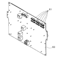
- a plurality of connectors 61 are provided on the main board 60, and a connector (not shown) provided at one end of the cable is connected to each connector 61. Is done.
- power is supplied from the main board 60 to the other board or data is transmitted between the main board and the other board. Is transmitted.
- the connectors (hereinafter also referred to as “cable-side connectors”) provided in the respective cables are a plurality of connectors (hereinafter also referred to as “substrate-side connectors”) provided on the main board. It takes time and effort to connect to each. Further, the cable side connector and the board side connector may be erroneously connected. Furthermore, when the cable-side connector is connected to the board-side connector or removed from the board-side connector, the cable-side connector may be inserted into the board-side connector or pulled out at an angle. If the connector is inserted at an angle or pulled out at an angle, the connector pin may be deformed or damaged. In particular, even if one of the plurality of connectors on the main board is damaged, the entire main board must be replaced.
- the connection structure of the present invention includes a support metal fitting to which the main board is attached and a shield metal fitting that accommodates the relay board.
- the support fitting is provided with a first opening that exposes a first connector provided on the main board, a first guide, and a pair of hinges.
- the shield metal fitting is provided with a second opening for exposing a second connector provided on the relay board, and a second guide part that cooperates with the first guide part.
- the first guide portion and the second guide portion are configured so that the shield metal fitting moves in a direction perpendicular to a main surface of the support metal fitting provided with the first opening. Guide the brackets.
- Each end of the pair of hinges is disposed between the shield metal fitting and the support metal fitting, and rotates to separate the shield metal from the support metal fitting.
- a plurality of cables can be simultaneously connected to the main board. Further, connector misconnection and connector pin breakage and deformation are prevented.
- connection structure is detachably attached to the main board.
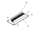
- FIG. 1A and 1B are perspective views of the relay board 10 according to the present embodiment.
- a plurality of distribution connectors 12 are provided on one surface (hereinafter referred to as “surface 11”) of the relay substrate 10 (in this embodiment, three pairs of distribution connectors 12 are provided.
- surface 11 the surface of the relay substrate 10
- three pairs of distribution connectors 12 are provided.
- FIG. 1B a common connector 14 electrically connected to each distribution connector 12 is provided on the other surface (hereinafter referred to as “back surface 13”) of the relay substrate 10. Further, through holes 15 are formed at the four corners of the relay substrate 10.
- FIGS. 2A and 2B are perspective views of the shield metal fitting 20 in which the relay board 10 is accommodated.
- the shield fitting 20 is made of metal and has a box shape with one side opened.
- the shield fitting 20 is formed in a box shape by a substantially rectangular bottom portion 21 and four side walls 22 rising vertically from each side of the bottom portion 21.
- an opening 23 for exposing the common connector 14 (FIG. 1B) provided on the relay board 10 is formed at the bottom 21 of the shield metal fitting 20.
- two holes 24 penetrating the bottom portion 21 are formed in the bottom portion 21 of the shield fitting 20.
- a metal guide tube 25 communicating with the hole 24 shown in FIG. In other words, two guide cylinders 25 that are parallel to each other are erected on the inner surface of the bottom of the shield fitting 20.
- the hole 24 and the guide cylinder 25 have the same inner diameter, and the central axes of the hole 24 and the guide cylinder 25 coincide with each other.
- screw holes 26 corresponding to the through holes 15 (FIG. 1A) provided in the relay substrate 10 are formed around the opening 23 provided in the bottom portion 21 of the shield metal 20. Is provided.
- the relay board 10 is accommodated and fixed inside the shield metal fitting 20 having the above structure.
- the relay substrate 10 is accommodated in the shield metal 20 with the back surface 13 facing the bottom inner surface of the shield metal 20.
- the common connector 14 (FIG. 1B) provided on the back surface 13 of the relay substrate 10 and the opening 23 (FIG. 2B) formed in the bottom 21 of the shield metal fitting 20 are aligned, and the common connector 14 is aligned. Is fitted into the opening 23.
- screws 16 (FIG. 6B) are inserted into the through holes 15 at the four corners of the relay substrate 10, and the inserted screws are screwed into the screw holes 26 provided in the bottom portion 21 of the shield fitting 20.
- the relay board 10 is accommodated in the shield fitting 20 and fixed (see FIG. 6B).
- the common connector 14 provided on the relay board 10 is exposed from the opening 23 of the shield metal fitting 20 (see FIG. 6A).
- 3A and 3B are perspective views of the support fitting 30 to which the main board is attached.
- the main board is fixed to the back side of the main surface 31 of the illustrated support fitting 30. For this reason, only the main connector 40 provided on the main board appears in FIGS. 3A and 3B, and the main board itself does not appear.
- the support metal fitting 30 is made of metal, and the main surface 31 is formed with an opening 32 through which the main connector 40 provided on the main board fixed on the back side of the main surface is exposed.
- a pair of L-shaped hinges 50 are provided symmetrically on the main surface front side shown in the figure. Specifically, a pair of hinges 50 are provided on both outer sides in the longitudinal direction of the opening 32.
- Each hinge 50 includes an action part 51 and an operation part 52 that extends from one end of the action part 51 at a right angle to the action part 51.
- Each hinge 50 is rotatably supported at a corner between the action portion 51 and the operation portion 52 by a rotation shaft 54 (FIG. 8) fixed to a bracket 53 fixed to the main surface of the support fitting 30. ing.
- each hinge 50 is arranged between the shield metal fitting 20 and the support metal fitting 30 when the relay board 10 and the main board are connected. Detailed operation of the hinge 50 will be described later.
- two metal guide pins 33 inserted into the guide tube 25 (FIG. 2A) of the shield metal fitting 20 stand perpendicular to the main surface 31 on the front surface side of the support metal fitting 30.
- two guide pins 33 that are parallel to each other are erected on the front surface side of the support metal 30.
- the bottom 21 of the shield metal 20 to which the relay substrate 10 is fixed is directed to the front surface side of the support metal 30, and the tip of the guide pin 33 protruding from the support metal 30 is placed on the shield metal 20. It inserts in the hole 24 (FIG. 2B) formed in the bottom part 21.
- the length (H) of the guide pin 33 shown in FIG. 3A is the projection length (h1) of the main connector 40 with respect to the main surface 31 of the support fitting 30 shown in the figure, and the bottom of the shield fitting 20 shown in FIG. 6A.
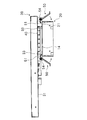
- the shield fitting 20 is brought close to the support fitting 30 according to the guide by the guide pin 33 and the guide tube 25 (FIG. 2A). Then, the bottom outer surface of the shield metal 20 comes into contact with the action portion 51 of the hinge 50.
- the action part 51 of the hinge 50 is pushed against the outer surface of the bottom of the shield metal 20, and the hinge 50 rotates inward about the rotation shaft 54 (in FIG. 4). Further, the common connector 14 protruding from the opening 23 of the shield metal 20 abuts on the main connector 40 protruding from the opening 32 of the support metal 30.
- the common connector 14 is connected to the main connector 40.
- the shield between the time when the distal end of the guide pin 33 is inserted into the hole 24 formed in the bottom 21 of the shield metal fitting 20 and the time when the common connector 14 is connected to the main connector 40.
- the metal fitting 20 moves in parallel while being guided by the guide pin 33 and the guide tube 25.
- the shield metal 20 moves perpendicularly to the main surface 31 of the support metal 30. Therefore, the common connector 14 is directly connected to the main connector 40.
- FIG. 5 shows a state where the common connector 14 and the main connector 40 are completely connected.
- the hinge 50 rotates to a position where the operation portion 52 is substantially perpendicular to the main surface 31 of the support fitting 30.
- the hinge 50 rotates to a position where the operation portion 52 is substantially parallel to the side wall 22 of the shield metal fitting 20.
- FIGS. 6A and 6B show enlarged views of the hinge 50 rotated to the position shown in FIG.
- FIG. 6A and FIG. 6B illustration of a support metal fitting is omitted for convenience.
- the action part 51 of the hinge 50 is opposed to the bottom 21 of the shield metal 20 and the main surface 31 of the support metal 30 (FIG. 5). It is sandwiched between.
- the operation portion 52 of the hinge 50 is provided with a protrusion (fixing portion 55) extending substantially perpendicularly from the operation portion 52.
- the fixing portion 55 covers the end face of the side wall 22 of the shield fitting 20 to prevent the common connector 14 (FIG. 1B) from coming off.
- the left and right hinges 50 are opened outwardly by pushing a bending portion 56 provided at the tip of the operation portion 52 of the hinge 50.
- the left and right hinges 50 are each rotated in the direction of the arrow.
- the bottom portion 21 of the shield fitting 20 is pushed by the action portion 51 of the hinge 50.
- the common connector 14 is pulled out from the main connector 40 by the lever principle. Therefore, the common connector 14 can be pulled out from the main connector 40 with a small force. Further, the shield fitting 20 moves in parallel while being guided by the guide pin 33 and the guide tube 25 (FIG. 2A). In other words, the shield metal 20 moves perpendicularly to the main surface 31 of the support metal 30. Therefore, the common connector 14 is pulled out straight from the main connector 40. In short, the common connector 14 can be pulled out straight from the main connector 40 with a small force.
- the guide pin 33 has a length that remains in the guide tube 25 even after the common connector 14 is pulled out from the main connector 40. Therefore, even after the connection between the common connector 14 and the main connector 40 is released, the shield fitting 20 is supported by the guide pins 33 and does not fall off.
- the distribution connector 12 provided on the relay board 10 connected to the main connector 40 is surrounded by the shield metal fitting 20. Therefore, leakage of electromagnetic waves radiated from cables (not shown) connected to these distribution connectors 12 is suppressed.
- the guide pin 33 (FIG. 3A) provided on the support fitting 30 is inserted into the guide cylinder 25 (FIG. 2A) provided on the shield fitting 20 as described above. It is as follows. Furthermore, the metal guide tube 25 and the metal guide pin 30 are electrically connected. In other words, the relay substrate 10 is electrically connected to the fixed substrate 30 via the shield fitting 20. As a result, the ground connection of the relay substrate 10 becomes more reliable, and the leakage of electromagnetic waves is further suppressed.
- the bracket 53 that supports the hinge 50 is provided with a stopper 57 that restricts the rotation of the hinge 50.
- the stopper 57 restricts the amount of rotation to the inside of the hinge 50. Specifically, the rotation amount of the hinge 50 is restricted so that the interval between the opposing hinges 50, more specifically the interval between the opposing operation units 52, does not become narrower than the width of the shield fitting 20.
Landscapes
- Details Of Connecting Devices For Male And Female Coupling (AREA)
Abstract
Priority Applications (3)
| Application Number | Priority Date | Filing Date | Title |
|---|---|---|---|
| PCT/JP2009/068667 WO2011052068A1 (fr) | 2009-10-30 | 2009-10-30 | Structure de connexion de substrat |
| CN200980161967.5A CN102648554B (zh) | 2009-10-30 | 2009-10-30 | 基板连接结构 |
| US13/502,947 US8585414B2 (en) | 2009-10-30 | 2009-10-30 | Substrate connecting structure |
Applications Claiming Priority (1)
| Application Number | Priority Date | Filing Date | Title |
|---|---|---|---|
| PCT/JP2009/068667 WO2011052068A1 (fr) | 2009-10-30 | 2009-10-30 | Structure de connexion de substrat |
Publications (1)
| Publication Number | Publication Date |
|---|---|
| WO2011052068A1 true WO2011052068A1 (fr) | 2011-05-05 |
Family
ID=43921509
Family Applications (1)
| Application Number | Title | Priority Date | Filing Date |
|---|---|---|---|
| PCT/JP2009/068667 Ceased WO2011052068A1 (fr) | 2009-10-30 | 2009-10-30 | Structure de connexion de substrat |
Country Status (3)
| Country | Link |
|---|---|
| US (1) | US8585414B2 (fr) |
| CN (1) | CN102648554B (fr) |
| WO (1) | WO2011052068A1 (fr) |
Families Citing this family (7)
| Publication number | Priority date | Publication date | Assignee | Title |
|---|---|---|---|---|
| WO2010067451A1 (fr) * | 2008-12-12 | 2010-06-17 | Necディスプレイソリューションズ株式会社 | Projecteur et unité pour projecteur |
| US8575480B2 (en) * | 2010-04-30 | 2013-11-05 | Delta Systems, Inc. | Connection assembly |
| US9166337B2 (en) * | 2012-12-18 | 2015-10-20 | Nvidia Corporation | Externally latching I/O housing |
| JP6274054B2 (ja) * | 2014-09-10 | 2018-02-07 | 株式会社デンソー | 基板接続構造 |
| CN105792515A (zh) * | 2014-12-25 | 2016-07-20 | 台达电子工业股份有限公司 | 电路板组合及其组装方法 |
| US9525257B1 (en) * | 2015-06-05 | 2016-12-20 | Acertara Acoustic Laboratories Llc | Universal adapter for ultrasonic probe connectors |
| JP7033990B2 (ja) * | 2018-04-09 | 2022-03-11 | 株式会社デンソーテン | 電子機器及びシャント抵抗固定構造 |
Citations (6)
| Publication number | Priority date | Publication date | Assignee | Title |
|---|---|---|---|---|
| JPH02106860U (fr) * | 1989-02-14 | 1990-08-24 | ||
| JPH04147588A (ja) * | 1990-10-08 | 1992-05-21 | Canon Inc | プリント配線基板装置 |
| JPH06140097A (ja) * | 1992-10-27 | 1994-05-20 | Fujitsu Ltd | 電子機器の接続構造 |
| JP2001265464A (ja) * | 2000-03-21 | 2001-09-28 | Matsushita Electric Ind Co Ltd | 情報処理装置 |
| JP2007157984A (ja) * | 2005-12-05 | 2007-06-21 | Denso Corp | 基板の接合方法 |
| JP2007234736A (ja) * | 2006-02-28 | 2007-09-13 | Icom Inc | 回路基板 |
Family Cites Families (21)
| Publication number | Priority date | Publication date | Assignee | Title |
|---|---|---|---|---|
| JPH02106860A (ja) | 1988-10-14 | 1990-04-18 | Nec Corp | 蛍光表示管 |
| US5268820A (en) * | 1992-08-18 | 1993-12-07 | Mitac International Corp. | Mother board assembly |
| JPH0697681A (ja) | 1992-09-17 | 1994-04-08 | Toshiba Corp | プリント配線板の抜止構造 |
| JPH08125301A (ja) | 1994-10-20 | 1996-05-17 | Fujitsu Ltd | 中継基板の実装構造 |
| JPH09689A (ja) | 1995-06-21 | 1997-01-07 | Sophia Co Ltd | 遊技機 |
| US5863211A (en) * | 1996-12-12 | 1999-01-26 | International Business Machines Corporation | Inter-book-package mechanical and electrical connection system |
| JP3830089B2 (ja) | 2001-12-17 | 2006-10-04 | 株式会社ケンウッド | パネル可倒機構 |
| US6951466B2 (en) * | 2003-09-02 | 2005-10-04 | Hewlett-Packard Development Company, L.P. | Attachment plate for directly mating circuit boards |
| JP4387832B2 (ja) | 2004-02-26 | 2009-12-24 | 富士通コンポーネント株式会社 | 平衡伝送用ケーブルコネクタ |
| CN2731906Y (zh) * | 2004-07-27 | 2005-10-05 | 銧达科技股份有限公司 | 电源转接模块 |
| US20060079113A1 (en) * | 2004-10-13 | 2006-04-13 | Fci Americas Technology, Inc. | Electrical connector spacer |
| US7326092B2 (en) * | 2005-08-11 | 2008-02-05 | Tyco Electronics Corporation | Double ended guide pin assembly |
| US7258569B1 (en) * | 2006-03-30 | 2007-08-21 | Emc Corporation | Connector-alignment collar for blind mating electrical connectors |
| US7589974B2 (en) * | 2006-04-21 | 2009-09-15 | Helwett-Packard Development Company, L.P. | Modular server and method |
| JP4480185B2 (ja) * | 2007-11-16 | 2010-06-16 | 日本航空電子工業株式会社 | コネクタ |
| CN101604804B (zh) * | 2008-06-10 | 2012-06-13 | 鸿富锦精密工业(深圳)有限公司 | 插座及应用该插座的插头插座装置 |
| TWI472398B (zh) * | 2008-09-30 | 2015-02-11 | Applied Materials Inc | 自校準之設施自動耦接器 |
| JP5090432B2 (ja) * | 2009-12-21 | 2012-12-05 | ヒロセ電機株式会社 | 電気コネクタの嵌合案内部品及びこれを有する電気コネクタ装置 |
| US8292629B2 (en) * | 2010-06-01 | 2012-10-23 | Tyco Electronics Corporation | Symmetric header connector |
| US20120149223A1 (en) * | 2010-12-13 | 2012-06-14 | 3M Innovative Properties Company | Electrical connector having lever |
| TWI457057B (zh) * | 2011-11-30 | 2014-10-11 | Ibm | 電路板總成,具有電路板總成的電子設備,及其升降裝置 |
-
2009
- 2009-10-30 US US13/502,947 patent/US8585414B2/en not_active Expired - Fee Related
- 2009-10-30 WO PCT/JP2009/068667 patent/WO2011052068A1/fr not_active Ceased
- 2009-10-30 CN CN200980161967.5A patent/CN102648554B/zh not_active Expired - Fee Related
Patent Citations (6)
| Publication number | Priority date | Publication date | Assignee | Title |
|---|---|---|---|---|
| JPH02106860U (fr) * | 1989-02-14 | 1990-08-24 | ||
| JPH04147588A (ja) * | 1990-10-08 | 1992-05-21 | Canon Inc | プリント配線基板装置 |
| JPH06140097A (ja) * | 1992-10-27 | 1994-05-20 | Fujitsu Ltd | 電子機器の接続構造 |
| JP2001265464A (ja) * | 2000-03-21 | 2001-09-28 | Matsushita Electric Ind Co Ltd | 情報処理装置 |
| JP2007157984A (ja) * | 2005-12-05 | 2007-06-21 | Denso Corp | 基板の接合方法 |
| JP2007234736A (ja) * | 2006-02-28 | 2007-09-13 | Icom Inc | 回路基板 |
Also Published As
| Publication number | Publication date |
|---|---|
| CN102648554B (zh) | 2015-02-18 |
| CN102648554A (zh) | 2012-08-22 |
| US8585414B2 (en) | 2013-11-19 |
| US20120208387A1 (en) | 2012-08-16 |
Similar Documents
| Publication | Publication Date | Title |
|---|---|---|
| WO2011052068A1 (fr) | Structure de connexion de substrat | |
| TWI553965B (zh) | 用於電氣連接器之插座 | |
| US8182294B2 (en) | Connector assembly and related methods of use | |
| KR20100023851A (ko) | 미리 종단된 시스템용 커넥터 어셈블리 | |
| JP4776483B2 (ja) | コネクタ実装構造 | |
| US20150103488A1 (en) | Cable support apparatus and information processing apparatus | |
| CN101926057A (zh) | 连接器保持装置 | |
| TWI628995B (zh) | 具有固定塊之纜線背板系統 | |
| US11469548B2 (en) | Cable connector | |
| US7738262B2 (en) | Plug-in unit and communication apparatus | |
| CN119322554B (zh) | 一种服务器和服务器组装方法 | |
| JP4729624B2 (ja) | ストレインリリーフを有する電気コネクタアダプタ | |
| TW201832420A (zh) | 機構件、使用該機構件之方法、具有該機構件之系統及組件 | |
| US9553404B2 (en) | Guide pins for connector assemblies | |
| CN101740911A (zh) | 连接器装置及使用该连接器装置的电子设备 | |
| JP2011124414A (ja) | 電子装置 | |
| CN201498776U (zh) | 电连接器 | |
| JP2013235808A (ja) | コネクタ、当該コネクタに用いられるリード線付ハウジング、ハウジングおよびコンタクト | |
| KR20120113523A (ko) | 록킹 부재를 구비한 플랫 케이블 접속용 커넥터 | |
| JP5333019B2 (ja) | 電気コネクタ | |
| JP6733498B2 (ja) | ケーブルユニット及びサーバ装置 | |
| JP7541144B1 (ja) | 接続構造および電子基板 | |
| JP7341050B2 (ja) | 電子機器 | |
| JP2001217039A (ja) | 多芯コネクタ | |
| JP5398032B2 (ja) | 筐体 |
Legal Events
| Date | Code | Title | Description |
|---|---|---|---|
| WWE | Wipo information: entry into national phase |
Ref document number: 200980161967.5 Country of ref document: CN |
|
| 121 | Ep: the epo has been informed by wipo that ep was designated in this application |
Ref document number: 09850847 Country of ref document: EP Kind code of ref document: A1 |
|
| WWE | Wipo information: entry into national phase |
Ref document number: 13502947 Country of ref document: US |
|
| NENP | Non-entry into the national phase |
Ref country code: DE |
|
| 122 | Ep: pct application non-entry in european phase |
Ref document number: 09850847 Country of ref document: EP Kind code of ref document: A1 |
|
| NENP | Non-entry into the national phase |
Ref country code: JP |