WO2011102059A1 - 金属積層構造体および金属積層構造体の製造方法 - Google Patents
金属積層構造体および金属積層構造体の製造方法 Download PDFInfo
- Publication number
- WO2011102059A1 WO2011102059A1 PCT/JP2010/073556 JP2010073556W WO2011102059A1 WO 2011102059 A1 WO2011102059 A1 WO 2011102059A1 JP 2010073556 W JP2010073556 W JP 2010073556W WO 2011102059 A1 WO2011102059 A1 WO 2011102059A1
- Authority
- WO
- WIPO (PCT)
- Prior art keywords
- metal layer
- metal
- layer
- tungsten
- laminated structure
- Prior art date
- Legal status (The legal status is an assumption and is not a legal conclusion. Google has not performed a legal analysis and makes no representation as to the accuracy of the status listed.)
- Ceased
Links
Images


Classifications
-
- H—ELECTRICITY
- H10—SEMICONDUCTOR DEVICES; ELECTRIC SOLID-STATE DEVICES NOT OTHERWISE PROVIDED FOR
- H10W—GENERIC PACKAGES, INTERCONNECTIONS, CONNECTORS OR OTHER CONSTRUCTIONAL DETAILS OF DEVICES COVERED BY CLASS H10
- H10W40/00—Arrangements for thermal protection or thermal control
- H10W40/20—Arrangements for cooling
- H10W40/25—Arrangements for cooling characterised by their materials
- H10W40/255—Arrangements for cooling characterised by their materials having a laminate or multilayered structure, e.g. direct bond copper [DBC] ceramic substrates
-
- C—CHEMISTRY; METALLURGY
- C25—ELECTROLYTIC OR ELECTROPHORETIC PROCESSES; APPARATUS THEREFOR
- C25D—PROCESSES FOR THE ELECTROLYTIC OR ELECTROPHORETIC PRODUCTION OF COATINGS; ELECTROFORMING; APPARATUS THEREFOR
- C25D5/00—Electroplating characterised by the process; Pretreatment or after-treatment of workpieces
- C25D5/10—Electroplating with more than one layer of the same or of different metals
-
- B—PERFORMING OPERATIONS; TRANSPORTING
- B32—LAYERED PRODUCTS
- B32B—LAYERED PRODUCTS, i.e. PRODUCTS BUILT-UP OF STRATA OF FLAT OR NON-FLAT, e.g. CELLULAR OR HONEYCOMB, FORM
- B32B15/00—Layered products comprising a layer of metal
- B32B15/01—Layered products comprising a layer of metal all layers being exclusively metallic
-
- C—CHEMISTRY; METALLURGY
- C22—METALLURGY; FERROUS OR NON-FERROUS ALLOYS; TREATMENT OF ALLOYS OR NON-FERROUS METALS
- C22C—ALLOYS
- C22C27/00—Alloys based on rhenium or a refractory metal not mentioned in groups C22C14/00 or C22C16/00
-
- C—CHEMISTRY; METALLURGY
- C22—METALLURGY; FERROUS OR NON-FERROUS ALLOYS; TREATMENT OF ALLOYS OR NON-FERROUS METALS
- C22C—ALLOYS
- C22C27/00—Alloys based on rhenium or a refractory metal not mentioned in groups C22C14/00 or C22C16/00
- C22C27/04—Alloys based on tungsten or molybdenum
-
- C—CHEMISTRY; METALLURGY
- C22—METALLURGY; FERROUS OR NON-FERROUS ALLOYS; TREATMENT OF ALLOYS OR NON-FERROUS METALS
- C22C—ALLOYS
- C22C9/00—Alloys based on copper
-
- C—CHEMISTRY; METALLURGY
- C25—ELECTROLYTIC OR ELECTROPHORETIC PROCESSES; APPARATUS THEREFOR
- C25D—PROCESSES FOR THE ELECTROLYTIC OR ELECTROPHORETIC PRODUCTION OF COATINGS; ELECTROFORMING; APPARATUS THEREFOR
- C25D3/00—Electroplating: Baths therefor
- C25D3/66—Electroplating: Baths therefor from melts
-
- C—CHEMISTRY; METALLURGY
- C25—ELECTROLYTIC OR ELECTROPHORETIC PROCESSES; APPARATUS THEREFOR
- C25D—PROCESSES FOR THE ELECTROLYTIC OR ELECTROPHORETIC PRODUCTION OF COATINGS; ELECTROFORMING; APPARATUS THEREFOR
- C25D5/00—Electroplating characterised by the process; Pretreatment or after-treatment of workpieces
- C25D5/10—Electroplating with more than one layer of the same or of different metals
- C25D5/12—Electroplating with more than one layer of the same or of different metals at least one layer being of nickel or chromium
-
- C—CHEMISTRY; METALLURGY
- C25—ELECTROLYTIC OR ELECTROPHORETIC PROCESSES; APPARATUS THEREFOR
- C25D—PROCESSES FOR THE ELECTROLYTIC OR ELECTROPHORETIC PRODUCTION OF COATINGS; ELECTROFORMING; APPARATUS THEREFOR
- C25D5/00—Electroplating characterised by the process; Pretreatment or after-treatment of workpieces
- C25D5/60—Electroplating characterised by the structure or texture of the layers
- C25D5/605—Surface topography of the layers, e.g. rough, dendritic or nodular layers
- C25D5/611—Smooth layers
-
- C—CHEMISTRY; METALLURGY
- C25—ELECTROLYTIC OR ELECTROPHORETIC PROCESSES; APPARATUS THEREFOR
- C25D—PROCESSES FOR THE ELECTROLYTIC OR ELECTROPHORETIC PRODUCTION OF COATINGS; ELECTROFORMING; APPARATUS THEREFOR
- C25D5/00—Electroplating characterised by the process; Pretreatment or after-treatment of workpieces
- C25D5/60—Electroplating characterised by the structure or texture of the layers
- C25D5/615—Microstructure of the layers, e.g. mixed structure
- C25D5/617—Crystalline layers
-
- H—ELECTRICITY
- H10—SEMICONDUCTOR DEVICES; ELECTRIC SOLID-STATE DEVICES NOT OTHERWISE PROVIDED FOR
- H10H—INORGANIC LIGHT-EMITTING SEMICONDUCTOR DEVICES HAVING POTENTIAL BARRIERS
- H10H20/00—Individual inorganic light-emitting semiconductor devices having potential barriers, e.g. light-emitting diodes [LED]
- H10H20/80—Constructional details
- H10H20/85—Packages
- H10H20/858—Means for heat extraction or cooling
- H10H20/8581—Means for heat extraction or cooling characterised by their material
-
- C—CHEMISTRY; METALLURGY
- C25—ELECTROLYTIC OR ELECTROPHORETIC PROCESSES; APPARATUS THEREFOR
- C25D—PROCESSES FOR THE ELECTROLYTIC OR ELECTROPHORETIC PRODUCTION OF COATINGS; ELECTROFORMING; APPARATUS THEREFOR
- C25D3/00—Electroplating: Baths therefor
- C25D3/02—Electroplating: Baths therefor from solutions
- C25D3/12—Electroplating: Baths therefor from solutions of nickel or cobalt
-
- C—CHEMISTRY; METALLURGY
- C25—ELECTROLYTIC OR ELECTROPHORETIC PROCESSES; APPARATUS THEREFOR
- C25D—PROCESSES FOR THE ELECTROLYTIC OR ELECTROPHORETIC PRODUCTION OF COATINGS; ELECTROFORMING; APPARATUS THEREFOR
- C25D3/00—Electroplating: Baths therefor
- C25D3/02—Electroplating: Baths therefor from solutions
- C25D3/38—Electroplating: Baths therefor from solutions of copper
-
- Y—GENERAL TAGGING OF NEW TECHNOLOGICAL DEVELOPMENTS; GENERAL TAGGING OF CROSS-SECTIONAL TECHNOLOGIES SPANNING OVER SEVERAL SECTIONS OF THE IPC; TECHNICAL SUBJECTS COVERED BY FORMER USPC CROSS-REFERENCE ART COLLECTIONS [XRACs] AND DIGESTS
- Y10—TECHNICAL SUBJECTS COVERED BY FORMER USPC
- Y10T—TECHNICAL SUBJECTS COVERED BY FORMER US CLASSIFICATION
- Y10T428/00—Stock material or miscellaneous articles
- Y10T428/12—All metal or with adjacent metals
- Y10T428/12493—Composite; i.e., plural, adjacent, spatially distinct metal components [e.g., layers, joint, etc.]
- Y10T428/12632—Four or more distinct components with alternate recurrence of each type component
-
- Y—GENERAL TAGGING OF NEW TECHNOLOGICAL DEVELOPMENTS; GENERAL TAGGING OF CROSS-SECTIONAL TECHNOLOGIES SPANNING OVER SEVERAL SECTIONS OF THE IPC; TECHNICAL SUBJECTS COVERED BY FORMER USPC CROSS-REFERENCE ART COLLECTIONS [XRACs] AND DIGESTS
- Y10—TECHNICAL SUBJECTS COVERED BY FORMER USPC
- Y10T—TECHNICAL SUBJECTS COVERED BY FORMER US CLASSIFICATION
- Y10T428/00—Stock material or miscellaneous articles
- Y10T428/12—All metal or with adjacent metals
- Y10T428/12493—Composite; i.e., plural, adjacent, spatially distinct metal components [e.g., layers, joint, etc.]
- Y10T428/12771—Transition metal-base component
- Y10T428/12806—Refractory [Group IVB, VB, or VIB] metal-base component
- Y10T428/12826—Group VIB metal-base component
- Y10T428/12833—Alternative to or next to each other
-
- Y—GENERAL TAGGING OF NEW TECHNOLOGICAL DEVELOPMENTS; GENERAL TAGGING OF CROSS-SECTIONAL TECHNOLOGIES SPANNING OVER SEVERAL SECTIONS OF THE IPC; TECHNICAL SUBJECTS COVERED BY FORMER USPC CROSS-REFERENCE ART COLLECTIONS [XRACs] AND DIGESTS
- Y10—TECHNICAL SUBJECTS COVERED BY FORMER USPC
- Y10T—TECHNICAL SUBJECTS COVERED BY FORMER US CLASSIFICATION
- Y10T428/00—Stock material or miscellaneous articles
- Y10T428/12—All metal or with adjacent metals
- Y10T428/12493—Composite; i.e., plural, adjacent, spatially distinct metal components [e.g., layers, joint, etc.]
- Y10T428/12771—Transition metal-base component
- Y10T428/12806—Refractory [Group IVB, VB, or VIB] metal-base component
- Y10T428/12826—Group VIB metal-base component
- Y10T428/1284—W-base component
-
- Y—GENERAL TAGGING OF NEW TECHNOLOGICAL DEVELOPMENTS; GENERAL TAGGING OF CROSS-SECTIONAL TECHNOLOGIES SPANNING OVER SEVERAL SECTIONS OF THE IPC; TECHNICAL SUBJECTS COVERED BY FORMER USPC CROSS-REFERENCE ART COLLECTIONS [XRACs] AND DIGESTS
- Y10—TECHNICAL SUBJECTS COVERED BY FORMER USPC
- Y10T—TECHNICAL SUBJECTS COVERED BY FORMER US CLASSIFICATION
- Y10T428/00—Stock material or miscellaneous articles
- Y10T428/12—All metal or with adjacent metals
- Y10T428/12493—Composite; i.e., plural, adjacent, spatially distinct metal components [e.g., layers, joint, etc.]
- Y10T428/12771—Transition metal-base component
- Y10T428/12861—Group VIII or IB metal-base component
- Y10T428/12903—Cu-base component
- Y10T428/1291—Next to Co-, Cu-, or Ni-base component
Definitions
- Patent Document 1 a layer made of a first material having high thermal conductivity such as copper (Cu) and a thermal expansion coefficient such as molybdenum (Mo) or tungsten (W) are small. Clad produced by joining a layer made of the second material with an applied pressure of 50 kgf / cm 2 to 150 kgf / cm 2 and a hot uniaxial working method (hot press method) at 850 ° C. to 1000 ° C. It is described that a material is used as a heat dissipation substrate for a semiconductor device (for example, paragraphs [0011], [0015], [0016], [0033], and [0034] of Patent Document 1).
- the second material due to the difference in deformation between the first material such as Cu and the second material such as Mo or W at the time of hot pressing.
- voids defects
- heat conduction in the vertical direction direction perpendicular to the surface of the heat dissipation substrate
- an object of the present invention is to provide a metal laminated structure and a metal laminated structure that can suppress thermal expansion in the horizontal direction and can improve heat conduction in the vertical direction. It is to provide a manufacturing method.
- the present invention includes a first metal layer containing tungsten, a second metal layer containing copper, and a third metal layer containing tungsten, the first metal layer being the second metal layer of the second metal layer.
- the third metal layer is disposed on the second surface opposite to the first surface of the second metal layer, and is formed of tungsten contained in the first metal layer.
- the crystal grains are columnar crystals extending in a direction perpendicular to the first surface of the second metal layer, and the tungsten crystal grains contained in the third metal layer are formed on the second surface of the second metal layer.
- it is a metal laminated structure which is a columnar crystal extending vertically.
- the metal laminated structure of the present invention preferably further comprises a metal layer containing at least one selected from the group consisting of cobalt, nickel, chromium and gold.
- the outermost surface of the metal laminate structure is a metal layer containing nickel, and a metal layer containing copper is provided inside the metal layer containing nickel.
- FIG. 1 is a schematic cross-sectional view of a metal laminated structure according to a first embodiment.
- 3 is a schematic enlarged cross-sectional view of an example of a first metal layer of the metal laminated structure according to Embodiment 1.
- FIG. 6 is a schematic enlarged cross-sectional view of another example of the first metal layer of the metal laminated structure according to Embodiment 1.
- FIG. 6 is a schematic enlarged cross-sectional view of still another example of the first metal layer of the metal laminated structure according to Embodiment 1.
- FIG. 5 is a schematic enlarged cross-sectional view of an example of a third metal layer of the metal laminated structure according to Embodiment 1.
- FIG. 6 is a schematic enlarged cross-sectional view of another example of the third metal layer of the metal multilayer structure according to Embodiment 1.
- FIG. 6 is a schematic enlarged cross-sectional view of still another example of the third metal layer of the metal multilayer structure according to Embodiment 1.
- FIG. 3 is a schematic configuration diagram illustrating an example of a method for manufacturing the metal laminated structure according to the first embodiment. It is a typical block diagram illustrating another example of the manufacturing method of the metal laminated structure of Embodiment 1.
- FIG. It is typical sectional drawing of an example of the LED element which is an example of the semiconductor device which used the metal laminated structure of Embodiment 1 as a heat sink.
- FIG. 5 is a schematic cross-sectional view of a metal laminated structure according to a second embodiment.
- FIG. 6 is a schematic configuration diagram illustrating an example of a method for manufacturing a metal laminated structure according to a second embodiment. It is a typical block diagram illustrating another example of the manufacturing method of the metal laminated structure of Embodiment 2.
- 6 is a schematic cross-sectional view of a metal laminated structure according to Embodiment 3.
- FIG. FIG. 6 is a schematic cross-sectional view of a metal laminated structure according to a fourth embodiment.
- FIG. 2 is a schematic configuration diagram of an apparatus used in Examples 1 to 4.
- Example 2 is a longitudinal cross-sectional photograph of a low-speed SEM in the vicinity of the interface between the tungsten layer and the copper layer of the metal multilayer structure of Example 1. It is an enlarged photograph of FIG. It is another longitudinal cross-sectional photograph of the low-speed SEM in the interface vicinity of the tungsten layer of a metal laminated structure of Example 1, and a copper layer.
- FIG. 1 shows a schematic cross-sectional view of a metal laminate structure of Embodiment 1 which is an example of the metal laminate structure of the present invention.
- the metal multilayer structure has a three-layer structure including a first metal layer 1 containing tungsten, a second metal layer 2 containing copper, and a third metal layer 3 containing tungsten. It is composed of
- the first metal layer 1 is disposed on the first surface 2 a that is one surface of the second metal layer 2, and the third metal layer 3 is the first of the second metal layer 2. It is installed on the second surface 2b which is the surface opposite to the surface 2a.
- the thickness T1 of the first metal layer 1 and the thickness T3 of the third metal layer 3 are 1 ⁇ m or more and 200 ⁇ m or less, respectively.
- the thickness T1 of the first metal layer 1 and the thickness T3 of the third metal layer 3 are each 1 ⁇ m or more and 200 ⁇ m or less, the columnar crystal is not affected by the crystal structure of the second metal layer 2. There is a tendency to obtain a dense structure having no voids in the layer.
- the thickness T2 of the second metal layer 2 is preferably 10 ⁇ m or more and 1500 ⁇ m or less.
- the thickness T2 of the second metal layer 2 is not less than 10 ⁇ m and not more than 1500 ⁇ m, deformation during the formation of the first metal layer 1 and the third metal layer 3 can be suppressed, and the metal laminated structure It exists in the tendency which can make the thickness of the whole body into the preferable range mentioned later.
- the total thickness T of the metal laminated structure is preferably 20 ⁇ m or more and 3000 ⁇ m or less.
- the metal laminate structure is excellent in handleability as a product because the appropriate strength is obtained, and the metal laminate structure such as a heat sink is used. It tends to be excellent in workability when it is necessary to join and cut another material on the body.
- the first metal layer with respect to the sum (T1 + T2 + T3) of the thickness T1 of the first metal layer 1, the thickness T2 of the second metal layer 2, and the thickness T3 of the third metal layer 3
- the ratio ((T1 + T3) / (T1 + T2 + T3)) of the sum (T1 + T3) of the thickness T1 of 1 and the thickness T3 of the third metal layer 3 is preferably 0.016 or more and 0.89 or less.
- the upper part from the central part in the thickness direction of the metal laminated structure (in this example, the half of the total thickness T of the metal laminated structure) It is preferable that a portion below the central portion in the thickness direction of the metal multilayer structure is symmetrical with respect to the central portion in the thickness direction of the metal multilayer structure.
- symmetry means that the material and thickness of the layer appearing when proceeding upward in the vertical direction from the center in the thickness direction of the metal laminate structure to the upper end surface is the center in the thickness direction of the metal laminate structure. It is a concept that includes not only the case where it is completely the same as the case of proceeding downward in the vertical direction from the part to the lower end surface but also the case where it is equivalent.
- FIG. 2 shows a schematic enlarged cross-sectional view of an example of the first metal layer 1 of the metal laminated structure of the first embodiment.
- FIG. 2 shows a longitudinal section of the metal laminated structure (a section in a direction perpendicular to the first surface 2 a of the second metal layer 2).
- the first metal layer 1 is composed of the second metal layer 2.
- a plurality of tungsten crystal grains 1a which are columnar crystals extending in a direction perpendicular to the first surface 2a of the first surface 2a are included.
- the tungsten crystal grains 1a in order for the tungsten crystal grains 1a to be “columnar crystals extending in a direction perpendicular to the first surface 2a”, the tungsten crystal grains in a direction in which the inclination with respect to the first surface 2a is 90 °.
- the aspect ratio (H1 / W1) which is the ratio between the length H1 of 1a and the length W1 of the tungsten crystal grain 1a in the direction in which the inclination with respect to the first surface 2a is 0 °, must be larger than 1. It is.
- Such an extension direction of the tungsten crystal grains 1 a is included in a range of 90 ° ⁇ 30 ° with respect to the first surface 2 a of the second metal layer 2, for example.
- FIG. 3 shows a schematic enlarged cross-sectional view of another example of the first metal layer 1 of the metal laminated structure according to the first embodiment.
- FIG. 3 shows a longitudinal section of the metal laminated structure (a section in a direction perpendicular to the first surface 2a of the second metal layer 2).
- the lengths H1 and W1 of the tungsten crystal grains 1a are respectively equal to the first surface 2a.
- the length in the direction in which the inclination with respect to is 90 ° and the length in the direction in which the inclination with respect to the first surface 2a is 0 °.
- the total number of tungsten crystal grains 1 a having an aspect ratio (H1 / W1) larger than 1 accounts for 50% or more of the total number of tungsten crystal grains constituting an arbitrary longitudinal section of the first metal layer 1. It is preferable that it occupies 70% or more.
- the total number of tungsten crystal grains 1a having an aspect ratio (H1 / W1) larger than 1 occupies 50% or more of the total number of tungsten crystal grains constituting an arbitrary longitudinal section of the first metal layer 1 In particular, when it occupies 70% or more, the thermal expansion in the horizontal direction of the metal structure tends to be further suppressed.
- FIG. 4 shows a schematic enlarged cross-sectional view of another example of the first metal layer 1 of the metal laminated structure of the first embodiment.
- FIG. 4 shows a region having a length of 500 ⁇ m in an arbitrary longitudinal section of the metal laminated structure (a section in a direction perpendicular to the first surface 2a of the second metal layer 2).
- a void 1b that is a dimple-like defect is formed on the surface of the first metal layer 1 on the first surface 2a side of the second metal layer 2.
- the number of voids 1b having a width Wb1 of an opening in an arbitrary longitudinal section of the metal laminated structure of 1 ⁇ m or more is 2 or less. Is preferable, more preferably 1 or less, and most preferably 0. When the number of voids 1b is 2 or less, when the number is 1 or less, particularly when it is 0, the heat conduction in the vertical direction of the metal laminated structure may be further improved. It tends to be possible.
- FIG. 5 shows a schematic enlarged cross-sectional view of an example of the third metal layer 3 of the metal laminated structure according to the first embodiment.
- FIG. 5 shows a vertical cross section (a cross section in a direction perpendicular to the second surface 2 b of the second metal layer 2) of the metal laminated structure, and the third metal layer 3 is the second metal layer 2.
- a plurality of tungsten crystal grains 3a which are columnar crystals extending in a direction perpendicular to the second surface 2b of the first surface 2b are included.
- the tungsten crystal grains 3a In order for the tungsten crystal grains 3a to be “columnar crystals extending in a direction perpendicular to the second surface 2b”, the tungsten crystal grains 3a in a direction in which the inclination with respect to the second surface 2b is 90 °. And the aspect ratio (H3 / W3), which is the ratio between the length H3 of the second crystal 2a and the length W3 of the tungsten crystal grain 3a in the direction in which the inclination with respect to the second surface 2b is 0 °, is required to be greater than 1. is there. Such an extension direction of the tungsten crystal grains 3 a is included in a range of 90 ° ⁇ 30 ° with respect to the second surface 2 b of the second metal layer 2, for example.
- FIG. 6 shows a schematic enlarged cross-sectional view of another example of the third metal layer 3 of the metal laminate structure of the first embodiment.
- the tungsten crystal grains 3 a constituting the third metal layer 3 are inclined with respect to the second surface 2 b of the second metal layer 2, the tungsten crystal grains 3 a
- the lengths H3 and W3 are respectively the length in the direction in which the inclination with respect to the second surface 2b is 90 ° and the length in the direction in which the inclination with respect to the second surface 2b is 0 °.
- the total number of tungsten crystal grains 3 a having an aspect ratio (H 3 / W 3) greater than 1 accounts for 50% or more of the total number of tungsten crystal grains constituting an arbitrary longitudinal section of the third metal layer 3. It is preferable that it occupies 70% or more.
- the total number of tungsten crystal grains 3a having an aspect ratio (H3 / W3) larger than 1 occupies 50% or more of the total number of tungsten crystal grains constituting an arbitrary longitudinal section of the third metal layer 3
- the thermal expansion in the horizontal direction of the metal structure tends to be further suppressed.
- FIG. 7 shows a schematic enlarged cross-sectional view of another example of the third metal layer 3 of the metal laminate structure of the first embodiment.
- FIG. 7 shows a region having a length of 500 ⁇ m in an arbitrary longitudinal section of the metal laminated structure (a section in a direction perpendicular to the second surface 2b of the second metal layer 2).
- a void 3b which is a dent-like defect is formed on the surface of the third metal layer 3 on the second surface 2b side of the second metal layer 2. Since the void 3b hinders heat conduction in the vertical direction of the metal laminated structure, the number of voids 3b having an opening width Wb3 of 1 ⁇ m or more in an arbitrary longitudinal section of the metal laminated structure is 2 or less. And most preferably 0. When the number of voids 3b is 2 or less, when it is 1 or less, particularly when it is 0, the heat conduction in the vertical direction of the metal laminated structure may be further improved. It tends to be possible.
- a molten salt bath 8 containing tungsten is accommodated in a container 7.
- the molten salt bath 8 is not particularly limited as long as tungsten can be deposited by electrolysis of the molten salt bath 8.
- potassium fluoride (KF) boron oxide (B 2 O 3 ), and tungsten oxide
- KF potassium fluoride
- B 2 O 3 boron oxide
- tungsten oxide for example, a molten salt bath prepared by melting a mixture prepared by mixing WO 3 ) with a molar ratio of 67: 26: 7 can be used.
- the second metal layer 2 such as a copper foil and the counter electrode 6 are immersed in the molten salt bath 8 accommodated in the container 7.
- the counter electrode 6 it is preferable to use an electrode made of tungsten that can maintain the ion balance of the bath by dissolution.
- a voltage is applied between the second metal layer 2 and the counter electrode 6 to electrolyze the molten salt bath 8.
- tungsten in the molten salt bath 8 is deposited on both surfaces of the second metal layer 2 respectively, and the first metal layer 1 containing tungsten and the third metal layer 3 containing tungsten.
- the second metal layer 2 after the formation of the first metal layer 1 and the third metal layer 3 is taken out of the molten salt bath 8, and the first metal layer 1 and the third metal, for example, with ion-exchanged water are used.
- the molten salt bath 8 adhering to each layer 3 is washed and removed. Then, for example, by washing with a predetermined acid, the oxide films formed on the surfaces of the first metal layer 1 and the third metal layer 3 are removed.
- the metal laminated structure of Embodiment 1 can be manufactured.
- the second metal layer 2 is made so that the second metal layer 2 such as a copper foil passes through the molten salt bath 8 accommodated in the container 7. It spans between the first roll 31a and the second roll 31b.
- the second metal layer 2 is fed out from the first roll 31a, and the molten salt bath 8 is electrolyzed while the second metal layer 2 is continuously immersed in the molten salt bath 8 accommodated in the container 7. .
- tungsten is deposited on both surfaces of the second metal layer 2 to form the first metal layer 1 containing tungsten and the third metal layer 3 containing tungsten.
- the metal laminated structure of Embodiment 1 can be manufactured.
- the first metal layer 1 and the third metal layer 3 formed by depositing tungsten on both surfaces of the second metal layer 2 are the second roll 31b. It is wound up and collected.
- the metal laminated structure of Embodiment 1 is not a conventional hot press method, but the first metal layer 1 containing tungsten on both surfaces of the second metal layer 2 containing copper by the molten salt plating as described above and The third metal layer 3 is formed and manufactured.
- the tungsten crystal grains 1a and 3a constituting the first metal layer 1 and the third metal layer 3 are formed. Each tends to be a columnar crystal extending in a direction perpendicular to the first surface 2 a and the second surface 2 b of the second metal layer 2.
- the extension directions of the tungsten crystal grains 1a and 3a constituting the first metal layer 1 and the third metal layer 3 are manufactured by a conventional hot press method.
- the second metal layer 2 tends to extend in a direction perpendicular to the first surface 2a and the second surface 2b of the second metal layer 2. Thermal expansion in the parallel direction (horizontal direction) can be suppressed with respect to the first surface 2a and the second surface 2b.
- the first metal layer 1 and the third metal layer 3 containing tungsten are formed on both surfaces of the second metal layer 2 containing copper by the molten salt plating as described above, Since the voids 1b and 3b are less likely to be formed on the surfaces of the first metal layer 1 and the third metal layer 3 constituting the interface with the metal layer 2, the first surface 2a and the second surface of the second metal layer 2 The heat conduction in the direction perpendicular to the surface 2b of 2 can be made favorable.
- the metal laminated structure of Embodiment 1 manufactured as described above can be used as, for example, a heat dissipation substrate (heat sink) for a semiconductor device.
- heat sink heat dissipation substrate
- FIG. 10 shows a schematic cross-sectional view of an example of an LED element which is an example of a semiconductor device using the metal laminated structure of the first embodiment as a heat dissipation substrate.
- the LED element shown in FIG. 10 includes the metal laminate structure 100 of the first embodiment and the LED structure 10 installed on the metal laminate structure 100.
- the metal laminate structure 100 and the LED structure 10 are included in the LED element. Are joined by a joining layer 21.
- the LED structure 10 is disposed on the semiconductor substrate 14, the n-type semiconductor layer 13 disposed on the semiconductor substrate 14, the active layer 12 disposed on the n-type semiconductor layer 13, and the active layer 12.
- the LED structure 10 includes a p-type semiconductor layer 11, an n-type semiconductor layer 13, and an active layer 12, and the active layer 12 is disposed between the p-type semiconductor layer 11 and the n-type semiconductor layer 13.
- any structure that emits light from the active layer 12 by current injection can be used without particular limitation.
- a conventionally known LED structure can be used.
- the p-type semiconductor layer 11, the active layer 12 and the n-type semiconductor layer 13 are each a group III element (at least one selected from the group consisting of Al, In and Ga) and a group V. It is preferable to use a group III-V nitride semiconductor which is a compound with an element (nitrogen). In this case, blue light can be emitted from the active layer 12.
- the LED structure 10 capable of emitting blue light from the active layer 12
- a GaN substrate or a sapphire substrate is used as the semiconductor substrate 14 shown in FIG. 10
- p-type GaN is used as the p-type semiconductor layer 11.
- An LED structure using an undoped InGaN layer as the active layer 12 and an n-type GaN layer as the n-type semiconductor layer 13 can be used.
- the metal laminated structure of the first embodiment is not limited to the LED element, and can be applied to a heat dissipation substrate for a semiconductor device other than the LED element such as a semiconductor laser element or a field effect transistor.
- a semiconductor substrate 14 used in the semiconductor device other than the LED structure 10 capable of emitting blue light from the active layer 12 for example, a silicon substrate, a silicon carbide substrate, a gallium arsenide substrate, or the like is used. Can do.
- the p-type semiconductor layer 11 is a semiconductor layer having a p-type conductivity type doped with a p-type impurity
- the n-type semiconductor layer 13 is an n-type conductivity type doped with an n-type impurity. Needless to say, this is a semiconductor layer.
- the active layer 12 may have either a p-type or n-type conductivity type, and is an undoped semiconductor layer in which neither p-type impurity nor n-type impurity is doped. Also good.
- the semiconductor substrate 14 and the n-type semiconductor layer 13 between the n-type semiconductor layer 13 and the active layer 12, between the active layer 12 and the p-type semiconductor layer 11, and between the p-type semiconductor layer 11 and the translucent electrode.
- Other layers may be included between at least one of the layers 17, between the translucent electrode 17 and the p-electrode 15, and between the n-type semiconductor layer 13 and the n-electrode 16.
- the bonding layer 21 for example, a layer made of a conductive material having a higher thermal conductivity than eutectic solder can be used.
- a metal that has low electrical resistance, high thermal conductivity, and is difficult to oxidize and in particular, at least one selected from the group consisting of gold, silver, copper, and nickel It is more preferable to use a layer containing.
- the n-electrode 16 of the LED element having the above configuration is used as a cathode, the p-electrode 15 is used as an anode, and a voltage is applied between these electrodes, whereby the p-electrode 15 to the n-electrode 16 are formed inside the LED structure 10.
- Current is passed toward Thereby, light can be generated in the active layer 12 between the p-type semiconductor layer 11 and the n-type semiconductor layer 13 of the LED structure 10.
- the LED element of the structure shown in FIG. 10 can be manufactured as follows, for example.
- the n-type semiconductor layer 13, the active layer 12 and the p-type semiconductor layer 11 are arranged in this order on the surface of the semiconductor substrate 14, for example. It is formed by epitaxial growth by MOCVD or the like.
- a semi-transparent electrode is formed on the p-type semiconductor layer 11 by using, for example, a lift-off method. 17 and p electrode 15 are formed, and n electrode 16 is formed on n type semiconductor layer 13.
- the metal laminated structure 100 of the first embodiment is bonded to the back surface of the semiconductor substrate 14 after the formation of the p electrode 15 and the n electrode 16 by the bonding layer 21.
- the semiconductor substrate 14 after the formation of the bonding layer 21 is cut by a circular rotary blade or the like to divide into individual LED elements having a schematic cross section shown in FIG. As described above, the LED element having the configuration shown in FIG. 10 can be obtained.
- the metal laminated structure 100 of the first embodiment can suppress the thermal expansion in the horizontal direction and can improve the heat conduction in the vertical direction. Therefore, when the metal laminated structure 100 according to the first embodiment is used as a heat dissipation substrate of a semiconductor device such as an LED element, the heat generation can be efficiently released to the outside while suppressing deformation due to heat generation of the semiconductor device. Very useful in that it can.
- FIG. 11 shows a schematic cross-sectional view of a metal laminated structure according to Embodiment 2, which is another example of the metal laminated structure of the present invention.
- the metal laminated structure of the second embodiment is the fourth metal layer 4 containing copper on the surface opposite to the second metal layer 2 side of the first metal layer 1 of the first embodiment.
- the thickness T4 of the fourth metal layer 4 and the thickness T5 of the fifth metal layer 5 are each preferably 10 ⁇ m or more and 500 ⁇ m or less.
- the thickness T4 of the fourth metal layer 4 and the thickness T5 of the fifth metal layer 5 are 10 ⁇ m or more and 500 ⁇ m or less, the surface roughness can be reduced and appropriate strength can be obtained. Therefore, it is excellent in the handleability as a product of a metal laminated structure and tends to be excellent in workability when it is necessary to join and cut another material on the metal laminated structure such as a heat sink. .
- the thickness T1 of the first metal layer 1, the thickness T2 of the second metal layer 2, the thickness T3 of the third metal layer 3, the thickness T4 of the fourth metal layer 4, Ratio (T1 + T3) of the sum (T1 + T3) of the thickness T3 of the first metal layer 1 and the thickness T3 of the third metal layer 3 to the sum (T1 + T2 + T3 + T4 + T5) of the thickness T5 of the fifth metal layer 5 [(T1 + T3) / (T1 + T2 + T3 + T4 + T5)] is preferably 0.015 or more and 0.89 or less.
- a molten salt bath 8 containing tungsten is prepared in a container 7, and the tungsten in the molten salt bath 8 is a second metal layer such as a copper foil. Precipitates on both sides of 2 respectively.
- a first metal layer 1 containing tungsten and a third metal layer 3 containing tungsten are formed on both surfaces of the second metal layer 2 by such molten salt bath plating.
- the second metal layer 2 after the formation of the first metal layer 1 and the third metal layer 3 is taken out from the molten salt bath 8, and the first metal layer 1 and the third metal layer 1 are removed with, for example, ion exchange water.
- the molten salt bath 8 adhering to the metal layer 3 is washed and removed. Then, for example, by washing with a predetermined acid, the oxide films formed on the surfaces of the first metal layer 1 and the third metal layer 3 are removed.
- the second metal layer 2 after the first metal layer 1 and the third metal layer 3 are formed in the electroplating solution 9 accommodated in the container 7.
- the counter electrode 6 is immersed.
- the electroplating solution 9 is not particularly limited as long as it contains copper, and for example, a commercially available copper sulfate plating solution can be used.
- the second metal layer 2 is used as a cathode and the counter electrode 6 is used as an anode
- a voltage is applied between the second metal layer 2 and the counter electrode 6 to electrolyze the electroplating solution 9.
- the copper in the electroplating solution 9 is deposited on the surface of the first metal layer 1 and the surface of the third metal layer 3 to form the fourth metal layer 4 and the fifth metal layer 5.
- the second metal layer 2 after the formation of the fourth metal layer 4 and the fifth metal layer 5 is taken out from the electroplating solution 9, and the fourth metal layer 4 and the fifth metal, for example, with ion-exchanged water are used.
- the electroplating solution 9 adhering to the layer 5 is removed by washing, and then the oxidation formed on the respective surfaces of the fourth metal layer 4 and the fifth metal layer 5 by washing with a predetermined acid, for example. Remove the membrane.
- the metal laminated structure of the second embodiment can be manufactured.
- a molten salt bath 8 in which a second metal layer 2 such as a copper foil is accommodated in a container 7 and an electroplating solution 9 accommodated in the container 7 respectively.
- the copper foil is passed between the first roll 31a and the second roll 31b so as to pass.
- the second metal layer 2 is fed out from the first roll 31a, and the molten salt bath 8 is electrolyzed while allowing the second metal layer 2 to pass through the molten salt bath 8 accommodated in the container 7.
- tungsten is deposited on both surfaces of the second metal layer 2 to form the first metal layer 1 and the third metal layer 3 on both surfaces of the second metal layer 2, respectively.
- the electroplating solution 9 is electrolyzed while passing the second metal layer 2 after the formation of the first metal layer 1 and the third metal layer 3 in the electroplating solution 9 accommodated in the container 7.
- the electrolytic plating copper is deposited on the surfaces of the first metal layer 1 and the third metal layer 3, respectively, and the fourth metal is deposited on the surfaces of the first metal layer 1 and the third metal layer 3, respectively.
- the metal layer 4 and the fifth metal layer 5 are formed, and the metal laminated structure of the second embodiment is manufactured.
- the metal laminated structure of the second embodiment is wound around the second roll 31b and collected.
- the fourth metal layer 4 and the fifth metal layer 5 were formed using the electroplating solution 9, respectively.
- the method for forming the fourth metal layer 4 and the fifth metal layer 5 is not limited thereto. Needless to say, it is not limited to.
- the fourth metal layer 4 and the fifth metal layer 5 can be formed by a conventionally known vapor phase method such as sputtering.
- the fourth metal layer 4 and the fifth metal layer 5 may be formed by combining, for example, formation of the electroplating solution by electrolysis and formation by a vapor phase method such as a sputtering method.
- the metal laminated structure is not limited to the above-described three-layer structure or five-layer structure, and includes three layers including the first metal layer 1, the second metal layer 2, and the third metal layer 3. Any structure having the above structure may be used, and an odd-numbered layer structure is preferable.
- FIG. 14 is a schematic cross-sectional view of a metal laminated structure according to Embodiment 3, which is another example of the metal laminated structure of the present invention.
- the metal laminated structure according to the third embodiment is provided between the first metal layer 1 and the fourth metal layer 4 of the metal laminated structure according to the second embodiment, and between the third metal layer 3 and the fifth metal.
- An adhesion layer 40 made of a metal layer containing at least one selected from the group consisting of cobalt (Co), nickel (Ni), chromium (Cr), and gold (Au) is further provided between the layers 5. It is characterized by being.
- the adhesion between the first metal layer 1 and the fourth metal layer 4 and the adhesion between the third metal layer 3 and the fifth metal layer 5 are provided. Since each force can be increased, the occurrence of delamination of the metal laminate structure can be suppressed.
- the metal laminated structure of Embodiment 3 can be manufactured, for example, as follows. First, the metal laminated structure of the first embodiment is manufactured as described above, and the first metal layer 1 and the third metal layer 3 of the metal laminated structure of the first embodiment are immersed in an alkaline solution. Thus, a degreasing process of the surface of the first metal layer 1 and the surface of the third metal layer 3 is performed.
- the first metal layer 1 and the third metal layer 3 are immersed in an alkaline aqueous solution as an anode and electrolysis is performed, so that the surface of the first metal layer 1 and the surface of the third metal layer 3 are removed. Each oxide film is removed.
- electrolysis is performed by immersing the first metal layer 1 and the third metal layer 3 after the removal of the oxide film as described above into a plating solution such as a cobalt sulfate aqueous solution. Thereby, a metal is deposited on the surface of the first metal layer 1 and the surface of the third metal layer 3 to form the adhesion layer 40.
- a plating solution such as a cobalt sulfate aqueous solution.
- the adhesion layer 40 formed as described above is used as a cathode to be immersed in a plating solution containing copper such as a copper sulfate plating solution for electrolysis. Thereby, copper is deposited on the surface of the adhesion layer 40 to form the fourth metal layer 4 and the fifth metal layer 5 containing copper, respectively.
- the metal laminated structure of Embodiment 3 can be manufactured.
- FIG. 15 is a schematic cross-sectional view of a metal laminated structure according to Embodiment 4, which is another example of the metal laminated structure of the present invention.
- the metal laminated structure of the fourth embodiment includes a metal layer 41 containing nickel, for example, on the surfaces of the fourth metal layer 4 and the fifth metal layer 5 of the metal laminated structure of the second embodiment. There is a special feature.
- the adhesion and reliability between the layers can be improved, and for example, resistance to processing and resistance to thermal shock can be ensured.
- the metal laminate structure of the fourth embodiment is obtained by, for example, immersing the metal laminate structure of the second embodiment manufactured as described above in a plating solution containing nickel and performing electrolysis. It can be formed by depositing nickel on the surfaces of the fourth metal layer 4 and the fifth metal layer 5 of the metal laminated structure.
- Example 1 After the KF powder and the WO 3 powder were sealed in the pressure vessel, the pressure vessel was kept at 500 ° C., and the inside of the pressure vessel was evacuated for 2 days or more to dry the KF powder and the WO 3 powder, respectively.
- the KF powder, the B 2 O 3 powder and the WO 3 powder after drying are put into the SiC crucible 111 which has been dried at 500 ° C. for 2 days or more so as to have the above molar ratio. Then, the crucible 111 in which these powders were charged was sealed in a quartz vacuum resistant container 110.
- the crucible 111 was held at 500 ° C. with the cover 118 made of SUS316L in the upper opening of the vacuum resistant container 110, and the inside of the vacuum resistant container 110 was evacuated for one day or more.
- lead wires 115 are respectively connected to the tungsten plate 113 and the copper plate 114, and tungsten wires are used for the lead wires 115 inside the vacuum resistant vessel 110, and the outside of the vacuum resistant vessel 110 is used.
- the lead wire 115 was a copper wire. Further, at least a part of the lead wire 115 was covered with an alumina covering material 116.
- the copper plate 114 after forming the tungsten layer is taken out from the apparatus shown in FIG. 16, and the surface of the tungsten layer is washed with hot water to remove the molten salt bath 8 adhering to the tungsten layer. -A tungsten laminate was obtained.
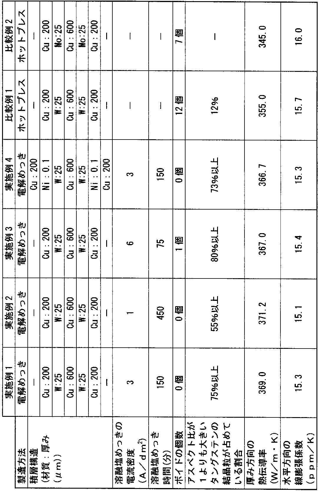
- the horizontal coefficient of linear expansion (ppm / ° C.) of the metal laminate structure of Example 1 was measured. The results are shown in Table 1. As shown in Table 1, the linear expansion coefficient in the horizontal direction of the metal laminated structure of Example 1 was 15.3 (ppm / ° C.). The horizontal coefficient of linear expansion (ppm / ° C.) was measured with a thermomechanical analyzer (TMA), measured from room temperature to 150 ° C., and the average value was calculated.
- TMA thermomechanical analyzer
- FIGS. FIG. 17 and FIG. 19 each show the vicinity of the interface between the tungsten layer and the copper layer of the metal laminated structure of Example 1, and FIG. 18 is an enlarged photograph of FIG.
- Example 2 A current having a current density of 1 A / dm 2 is passed between the tungsten plate 113 and the copper plate 114 for 450 minutes to perform constant-current electrolysis of the molten salt bath 8 to form a tungsten layer having a thickness of 25 ⁇ m on both sides of the copper plate 114.
- a metal laminated structure of Example 2 was produced in the same manner as Example 1 except that.
- the thermal conductivity in the thickness direction of the metal laminated structure of Example 2 is 371.2 (W / m ⁇ K), and the linear expansion coefficient in the horizontal direction is 15.1 (ppm / ° C. ),
- the aspect ratio was 3.4, and the number of voids was 0 (pieces).
- tungsten crystal grains having an aspect ratio larger than 1 accounted for 55% or more of the total number of tungsten crystal grains constituting the tungsten layer.
- Example 3 A current having a current density of 6 A / dm 2 is passed between the tungsten plate 113 and the copper plate 114 for 75 minutes to perform constant current electrolysis of the molten salt bath 8 to form a tungsten layer having a thickness of 25 ⁇ m on both sides of the copper plate 114.
- a metal laminated structure of Example 3 was produced in the same manner as Example 1 except that.
- Example 3 And about the metal laminated structure of Example 3 produced as mentioned above, it is the same as the metal laminated structure of Example 1, and heat conductivity (W / m * K) of a thickness direction, horizontal line The expansion coefficient (ppm / ° C.), the aspect ratio, and the number of voids (pieces) were determined. The results are shown in Table 1.
- Example 4 After a tungsten-copper-tungsten laminate was produced in the same manner as in Example 1, a nickel layer was formed on the surfaces of the tungsten layers formed on both surfaces of the copper plate 114 by electrolytic plating.
- the counter electrode was used as the anode
- the tungsten-copper-tungsten laminate was used as the cathode
- a current density of 10 A / dm 2 was passed between them for 3 minutes to perform electroplating at room temperature.
- nickel is deposited on the surfaces of the tungsten layers on both sides of the tungsten-copper-tungsten laminate to form an adhesion layer made of nickel having a thickness of 0.1 ⁇ m, and nickel-tungsten-copper-tungsten. -A nickel laminate was formed.
- Example 4 Thereafter, in the same manner as in Example 1, copper was deposited on each surface of the adhesion layer made of nickel by electroplating with a copper sulfate plating solution, and a copper-nickel-tungsten-copper-tungsten-nickel-copper laminate. The metal laminated structure of Example 4 was produced.
- Example 4 And about the metal laminated structure of Example 4 produced as mentioned above, it is the same as the metal laminated structure of Example 1, and heat conductivity (W / m * K) of a thickness direction, horizontal line The expansion coefficient (ppm / ° C.), the aspect ratio, and the number of voids (pieces) were determined. The results are shown in Table 1.
- the thermal conductivity in the thickness direction of the metal laminated structure of Example 4 is 366.7 (W / m ⁇ K), and the linear expansion coefficient in the horizontal direction is 15.3 (ppm / ° C. ), The aspect ratio was 5.4, and the number of voids was 0 (pieces).
- tungsten crystal grains having an aspect ratio larger than 1 accounted for 73% or more of the total number of tungsten crystal grains constituting the tungsten layer.
- the thermal conductivity in the thickness direction of the metal laminated structure of Comparative Example 1 is 355.0 (W / m ⁇ K), and the linear expansion coefficient in the horizontal direction is 15.7 (ppm / ° C.). ),
- the aspect ratio was 0.1, and the number of voids was 12 (pieces).
- tungsten crystal grains having an aspect ratio larger than 1 accounted for 12% of the total number of tungsten crystal grains constituting the tungsten layer.
- Comparative Example 2 Lamination of a five-layer structure of copper-molybdenum-copper-molybdenum-copper in the same manner as in Comparative Example 1 except that a commercially available rolled molybdenum foil having a thickness of 25 ⁇ m was used instead of a commercially available rolled tungsten foil having a thickness of 25 ⁇ m. A metal laminated structure of Comparative Example 2 made of a body was produced.
- the thermal conductivity in the thickness direction of the metal laminated structure of Comparative Example 2 is 345.0 (W / m ⁇ K), and the linear expansion coefficient in the horizontal direction is 16.0 (ppm / ° C.). ) And the number of voids was 7 (pieces).
- the aspect ratio of the tungsten crystal grains constituting the tungsten layer was 3.4 to 5.7. Met.
- tungsten crystal grains having an aspect ratio larger than 1 accounted for 50% or more of the total number of tungsten crystal grains constituting the tungsten layer.
- the aspect ratio of tungsten crystal grains constituting the tungsten layer was 0.1.
- tungsten crystal grains having an aspect ratio of 1 or less accounted for 50% or more of the total number of tungsten crystal grains constituting the tungsten layer.
- the metal laminated structures of Examples 1 to 4 in which the tungsten layer was formed by molten salt plating were compared with the metal laminated structure of Comparative Example 2 in which the molybdenum layer was formed by hot pressing.
- the coefficient of linear expansion in the horizontal direction was suppressed, and the thermal conductivity (W / m ⁇ K) in the thickness direction was high.
- the thickness direction It was confirmed that the thermal conductivity (W / m ⁇ K) can be increased and the linear expansion coefficient (ppm / ° C.) in the horizontal direction can be suppressed.
- the metal laminated structure and the method for producing the metal laminated structure of the present invention may be used for a heat sink of a semiconductor device, for example.
Landscapes
- Chemical & Material Sciences (AREA)
- Engineering & Computer Science (AREA)
- Metallurgy (AREA)
- Organic Chemistry (AREA)
- Materials Engineering (AREA)
- Electrochemistry (AREA)
- Chemical Kinetics & Catalysis (AREA)
- Mechanical Engineering (AREA)
- Crystallography & Structural Chemistry (AREA)
- Laminated Bodies (AREA)
- Cooling Or The Like Of Semiconductors Or Solid State Devices (AREA)
- Electroplating Methods And Accessories (AREA)
- Led Device Packages (AREA)
- Led Devices (AREA)
- Ceramic Engineering (AREA)
Abstract
Description
図1に、本発明の金属積層構造体の一例である実施の形態1の金属積層構造体の模式的な断面図を示す。ここで、金属積層構造体は、タングステンを含む第1の金属層1と、銅を含む第2の金属層2と、タングステンを含む第3の金属層3と、の3層構造の積層構造体から構成されている。
まず、図8の模式的構成図に示すように、タングステンを含む溶融塩浴8を容器7に収容する。溶融塩浴8は、溶融塩浴8の電解によりタングステンを析出することができるものであれば特に限定されないが、たとえば、フッ化カリウム(KF)と酸化ホウ素(B2O3)と酸化タングステン(WO3)とをたとえば67:26:7のモル比で混合した混合物を溶融して作製した溶融塩浴などを用いることができる。
まず、図9の模式的構成図に示すように、たとえば銅箔などの第2の金属層2が容器7に収容された溶融塩浴8中を通過するように、第2の金属層2を第1のロール31aと第2のロール31bとの間に掛け渡す。
図11に、本発明の金属積層構造体の他の一例である実施の形態2の金属積層構造体の模式的な断面図を示す。ここで、実施の形態2の金属積層構造体は、実施の形態1の第1の金属層1の第2の金属層2側とは反対側の表面上に銅を含む第4の金属層4が設置されているとともに、第3の金属層3の第2の金属層2側とは反対側の表面上に銅を含む第5の金属層5が設置されている5層構造とされている点に特徴がある。
まず、実施の形態1と同様に、図8に示すように、容器7中にタングステンを含む溶融塩浴8を準備し、溶融塩浴8中のタングステンをたとえば銅箔などの第2の金属層2の両面にそれぞれ析出させる。このような溶融塩浴めっきにより第2の金属層2の両面にそれぞれタングステンを含む第1の金属層1およびタングステンを含む第3の金属層3を形成する。
まず、図13の模式的構成図に示すように、たとえば銅箔などの第2の金属層2が容器7に収容された溶融塩浴8および容器7に収容された電気めっき液9中をそれぞれ通過するように銅箔を第1のロール31aと第2のロール31bとの間に掛け渡す。
図14に、本発明の金属積層構造体の他の一例である実施の形態3の金属積層構造体の模式的な断面図を示す。実施の形態3の金属積層構造体は、実施の形態2の金属積層構造体の第1の金属層1と第4の金属層4との間、および第3の金属層3と第5の金属層5との間にそれぞれ、コバルト(Co)、ニッケル(Ni)、クロム(Cr)および金(Au)からなる群から選択された少なくとも1種を含む金属層からなる密着層40をさらに備えていることを特徴とする。
まず、上述のようにして、実施の形態1の金属積層構造体を製造し、実施の形態1の金属積層構造体の第1の金属層1および第3の金属層3をアルカリ溶液に浸漬させることによって、第1の金属層1の表面および第3の金属層3の表面の脱脂工程を行なう。
図15に、本発明の金属積層構造体の他の一例である実施の形態4の金属積層構造体の模式的な断面図を示す。実施の形態4の金属積層構造体は、実施の形態2の金属積層構造体の第4の金属層4および第5の金属層5の表面にそれぞれ、たとえばニッケルを含む金属層41を備えていることに特徴がある。
KF粉末およびWO3粉末をそれぞれ耐圧容器に封入した後に、耐圧容器を500℃に保持し、耐圧容器の内部を2日間以上真空引きすることによってKF粉末およびWO3粉末をそれぞれ乾燥させた。
タングステン板113と銅板114との間に1A/dm2の電流密度の電流を450分間流して溶融塩浴8の定電流電解を行なって銅板114の両面にそれぞれ25μmの厚さのタングステン層を形成したこと以外は実施例1と同様にして実施例2の金属積層構造体を作製した。
タングステン板113と銅板114との間に6A/dm2の電流密度の電流を75分間流して溶融塩浴8の定電流電解を行なって銅板114の両面にそれぞれ25μmの厚さのタングステン層を形成したこと以外は実施例1と同様にして実施例3の金属積層構造体を作製した。
実施例1と同様にしてタングステン-銅-タングステンの積層体を作製した後に、銅板114の両面にそれぞれ形成されたタングステン層の表面に電解めっきによりニッケル層を形成した。
厚さ600μmの銅板の両面にそれぞれ、厚さ25μmの市販の圧延タングステン箔を設置し、さらに、両側の圧延タングステン箔のそれぞれの表面上に厚さ200μmの銅板を設置した積層体を作製した。
厚さ25μmの市販の圧延タングステン箔に代えて厚さ25μmの市販の圧延モリブデン箔を用いたこと以外は比較例1と同様にして、銅-モリブデン-銅-モリブデン-銅の5層構造の積層体からなる比較例2の金属積層構造体を作製した。
Claims (8)
- タングステンを含む第1の金属層(1)と、銅を含む第2の金属層(2)と、タングステンを含む第3の金属層(3)と、を備え、
前記第1の金属層(1)は前記第2の金属層(2)の第1の表面(2a)上に設置され、
前記第3の金属層(3)は前記第2の金属層(2)の前記第1の表面(2a)とは反対側の第2の表面(2b)上に設置されており、
前記第1の金属層(1)に含まれる前記タングステンの結晶粒(1a)は前記第2の金属層の前記第1の表面(2a)に対して垂直方向に伸長する柱状結晶であり、
前記第3の金属層(3)に含まれる前記タングステンの結晶粒(3a)が前記第2の金属層(2)の前記第2の表面(2b)に対して垂直方向に伸長する柱状結晶である、金属積層構造体(100)。 - 前記第1の金属層(1)の厚さおよび前記第3の金属層(3)の厚さがそれぞれ1μm以上200μm以下である、請求項1に記載の金属積層構造体(100)。
- 前記金属積層構造体(100)の縦断面における長さ500μmの領域内に存在する1μm以上のボイド(1b,3b)の個数が2個以下である、請求項1に記載の金属積層構造体(100)。
- 前記金属積層構造体(100)は3層以上の奇数層である、請求項1に記載に記載の金属積層構造体(100)。
- コバルト、ニッケル、クロムおよび金からなる群から選択された少なくとも1種を含む金属層(40)をさらに備えた、請求項1に記載に記載の金属積層構造体(100)。
- 前記金属積層構造体(100)の最表面が銅を含む金属層(4,5)である、請求項1に記載に記載の金属積層構造体(100)。
- 前記金属積層構造体(100)の最表面がニッケルを含む金属層(41)であり、前記ニッケルを含む金属層(41)の内側に銅を含む金属層(4,5)が設けられている、請求項1に記載に記載の金属積層構造体(100)。
- タングステンを含む第1の金属層(1)を銅を含む第2の金属層(2)の第1の表面(2a)上に溶融塩浴めっきにより形成する工程と、
タングステンを含む第3の金属層(3)を前記第2の金属層(2)の前記第1の表面(2a)とは反対側の第2の表面(2b)上に溶融塩浴めっきにより形成する工程と、を含む、金属積層構造体(100)の製造方法。
Priority Applications (4)
| Application Number | Priority Date | Filing Date | Title |
|---|---|---|---|
| US13/580,082 US8993121B2 (en) | 2010-02-19 | 2010-12-27 | Metal laminated structure and method for producing the same |
| KR1020127023924A KR101716924B1 (ko) | 2010-02-19 | 2010-12-27 | 금속 적층 구조체 및 금속 적층 구조체의 제조 방법 |
| EP10846190.6A EP2537963A4 (en) | 2010-02-19 | 2010-12-27 | METAL LAMINATE STRUCTURE AND MANUFACTURING METHOD THEREFOR |
| CN201080064177.8A CN102762779B (zh) | 2010-02-19 | 2010-12-27 | 金属叠层结构及其制造方法 |
Applications Claiming Priority (2)
| Application Number | Priority Date | Filing Date | Title |
|---|---|---|---|
| JP2010-034782 | 2010-02-19 | ||
| JP2010034782A JP5583985B2 (ja) | 2010-02-19 | 2010-02-19 | 金属積層構造体 |
Publications (1)
| Publication Number | Publication Date |
|---|---|
| WO2011102059A1 true WO2011102059A1 (ja) | 2011-08-25 |
Family
ID=44482668
Family Applications (1)
| Application Number | Title | Priority Date | Filing Date |
|---|---|---|---|
| PCT/JP2010/073556 Ceased WO2011102059A1 (ja) | 2010-02-19 | 2010-12-27 | 金属積層構造体および金属積層構造体の製造方法 |
Country Status (7)
| Country | Link |
|---|---|
| US (1) | US8993121B2 (ja) |
| EP (1) | EP2537963A4 (ja) |
| JP (1) | JP5583985B2 (ja) |
| KR (1) | KR101716924B1 (ja) |
| CN (1) | CN102762779B (ja) |
| TW (1) | TWI496681B (ja) |
| WO (1) | WO2011102059A1 (ja) |
Families Citing this family (8)
| Publication number | Priority date | Publication date | Assignee | Title |
|---|---|---|---|---|
| JP2013098481A (ja) * | 2011-11-04 | 2013-05-20 | Sumitomo Electric Device Innovations Inc | 半導体装置 |
| US20140069622A1 (en) * | 2012-07-09 | 2014-03-13 | Ko-Chun Chen | Heat dissipation composite and the use thereof |
| CN105798544B (zh) * | 2014-12-31 | 2018-10-02 | 北京有色金属研究总院 | 一种钨-铜复合材料及其制备方法 |
| WO2016111207A1 (ja) * | 2015-01-07 | 2016-07-14 | 新日鉄住金マテリアルズ株式会社 | 放熱基板 |
| CN110699724B (zh) * | 2019-09-18 | 2021-02-12 | 湖南纳菲尔新材料科技股份有限公司 | 一种高耐蚀镍钨基合金多层镀层及其制备工艺 |
| CN110983394B (zh) * | 2019-12-24 | 2021-02-19 | 湖南纳菲尔新材料科技股份有限公司 | 一种高强度紧固件高防腐电镀工艺 |
| JP7444814B2 (ja) * | 2021-04-27 | 2024-03-06 | Ngkエレクトロデバイス株式会社 | パッケージ |
| US12276017B2 (en) * | 2021-05-21 | 2025-04-15 | Vactronix Scientific, Llc | Engineered multi-dimensional metallurgical properties in PVD materials |
Citations (11)
| Publication number | Priority date | Publication date | Assignee | Title |
|---|---|---|---|---|
| JPH0280589A (ja) * | 1988-09-17 | 1990-03-20 | Nisshin Steel Co Ltd | 電気タングステンめっき浴およびその浴によるめっき方法 |
| JPH03218054A (ja) * | 1990-01-23 | 1991-09-25 | Mitsubishi Electric Corp | 発熱素子用基板 |
| JP2005097704A (ja) * | 2003-09-26 | 2005-04-14 | Honda Motor Co Ltd | 摺動部材 |
| JP2005105354A (ja) * | 2003-09-30 | 2005-04-21 | Honda Motor Co Ltd | 摺動部材 |
| WO2006038476A1 (ja) * | 2004-10-01 | 2006-04-13 | Sumitomo Electric Industries, Ltd. | 溶融塩浴、この溶融塩浴を用いて得られた析出物、金属製品の製造方法および金属製品 |
| JP2006127847A (ja) * | 2004-10-27 | 2006-05-18 | Sumitomo Electric Ind Ltd | 膜形成用配向基板および超電導線材 |
| JP3862737B1 (ja) | 2005-10-18 | 2006-12-27 | 栄樹 津島 | クラッド材およびその製造方法、クラッド材の成型方法、クラッド材を用いた放熱基板 |
| WO2008013279A1 (en) * | 2006-07-28 | 2008-01-31 | Kyocera Corporation | Electronic component storing package and electronic device |
| JP2008214728A (ja) * | 2007-03-07 | 2008-09-18 | Sumitomo Electric Ind Ltd | セラミックス膜の製造方法 |
| JP2009235462A (ja) * | 2008-03-26 | 2009-10-15 | Sumitomo Electric Ind Ltd | 溶融塩浴、溶融塩浴の製造方法およびタングステン析出物 |
| WO2011001795A1 (ja) * | 2009-06-30 | 2011-01-06 | 住友電気工業株式会社 | 金属積層構造体および金属積層構造体の製造方法 |
Family Cites Families (39)
| Publication number | Priority date | Publication date | Assignee | Title |
|---|---|---|---|---|
| US4025997A (en) * | 1975-12-23 | 1977-05-31 | International Telephone & Telegraph Corporation | Ceramic mounting and heat sink device |
| US4371589A (en) | 1976-08-24 | 1983-02-01 | Warner London Inc. | Process for depositing protective coating and articles produced |
| US4448854A (en) * | 1980-10-30 | 1984-05-15 | The United States Of America As Represented By The United States Department Of Energy | Coherent multilayer crystals and method of making |
| KR900005847B1 (ko) * | 1988-05-31 | 1990-08-13 | 삼성전관 주식회사 | 텅스텐 전극의 표면처리 방법 |
| JPH01305544A (ja) | 1988-06-03 | 1989-12-08 | Denki Kagaku Kogyo Kk | 半導体装置 |
| JPH02256262A (ja) | 1988-12-14 | 1990-10-17 | Sumitomo Metal Ind Ltd | 半導体素子用ヒートシンク |
| JPH04230063A (ja) | 1990-12-27 | 1992-08-19 | Aichi Steel Works Ltd | 多層ヒートシンク |
| JP2860037B2 (ja) | 1993-03-15 | 1999-02-24 | 東京タングステン株式会社 | 半導体装置用放熱基板の製造方法 |
| JPH07211822A (ja) | 1994-01-24 | 1995-08-11 | Kyocera Corp | 半導体素子収納用パッケージ |
| US5445106A (en) * | 1994-10-03 | 1995-08-29 | General Electric Company | Method for making high thermal conducting diamond |
| US5525815A (en) * | 1994-10-03 | 1996-06-11 | General Electric Company | Diamond film structure with high thermal conductivity |
| JPH08222658A (ja) | 1995-02-17 | 1996-08-30 | Sumitomo Electric Ind Ltd | 半導体素子用パッケージ及びその製造方法 |
| JPH1012767A (ja) | 1996-06-19 | 1998-01-16 | Tokyo Tungsten Co Ltd | 積層構造放熱基板及びその製造方法 |
| JPH11284111A (ja) | 1998-03-30 | 1999-10-15 | Sumitomo Special Metals Co Ltd | ヒートシンク部材及びその製造方法、並びにヒートシンク部材を用いた半導体パッケージ |
| JP2000124370A (ja) | 1998-10-15 | 2000-04-28 | Sumitomo Metal Electronics Devices Inc | 半導体装置用パッケージ |
| JP3505704B2 (ja) | 1999-05-10 | 2004-03-15 | 株式会社アライドマテリアル | 放熱基板およびその製造方法 |
| US6352014B1 (en) | 1999-12-15 | 2002-03-05 | International Business Machines Corporation | Method for making punches using multi-layer ceramic technology |
| US6965199B2 (en) | 2001-03-27 | 2005-11-15 | The University Of North Carolina At Chapel Hill | Coated electrode with enhanced electron emission and ignition characteristics |
| JP2003037204A (ja) | 2001-07-25 | 2003-02-07 | Kyocera Corp | 半導体素子収納用パッケージ |
| US20040140474A1 (en) | 2002-06-25 | 2004-07-22 | Matsushita Electric Industrial Co., Ltd. | Semiconductor light-emitting device, method for fabricating the same and method for bonding the same |
| JP2004088083A (ja) | 2002-06-25 | 2004-03-18 | Matsushita Electric Ind Co Ltd | 半導体発光素子、その製造方法及びその実装方法 |
| TW200500199A (en) * | 2003-02-12 | 2005-01-01 | Furukawa Circuit Foil | Copper foil for fine patterned printed circuits and method of production of same |
| JP2004249589A (ja) | 2003-02-20 | 2004-09-09 | Toshiba Corp | 銅−モリブデン複合材料およびそれを用いたヒートシンク |
| CN100584251C (zh) | 2003-08-13 | 2010-01-27 | 全包层金属制品公司 | 具有均匀传热特性的结合金属组件及其制造方法 |
| US7279407B2 (en) * | 2004-09-02 | 2007-10-09 | Micron Technology, Inc. | Selective nickel plating of aluminum, copper, and tungsten structures |
| JP2006100640A (ja) | 2004-09-30 | 2006-04-13 | Hitachi Metals Ltd | セラミックス回路基板及びこれを用いたパワー半導体モジュール |
| WO2006057231A1 (ja) * | 2004-11-24 | 2006-06-01 | Sumitomo Electric Industries, Ltd. | 溶融塩浴、析出物および金属析出物の製造方法 |
| US8318519B2 (en) | 2005-01-11 | 2012-11-27 | SemiLEDs Optoelectronics Co., Ltd. | Method for handling a semiconductor wafer assembly |
| US9390999B2 (en) | 2005-03-23 | 2016-07-12 | Noriaki Kawamura | Metal substrate/metal impregnated carbon composite material structure and method for manufacturing said structure |
| TWI254419B (en) | 2005-04-08 | 2006-05-01 | Univ Nat Chiao Tung | Compound semiconductor device having copper metallization |
| JP4711724B2 (ja) | 2005-04-19 | 2011-06-29 | 学校法人同志社 | 溶融塩めっき用電解浴及び該電解浴を用いた溶融塩めっき方法 |
| US7695808B2 (en) | 2005-11-07 | 2010-04-13 | 3M Innovative Properties Company | Thermal transfer coating |
| JP4867388B2 (ja) | 2006-02-21 | 2012-02-01 | トヨタ自動車株式会社 | 熱電発電装置 |
| JP2007327081A (ja) | 2006-06-06 | 2007-12-20 | Toyota Central Res & Dev Lab Inc | 接着方法、半導体装置の製造方法、及び半導体装置 |
| JP4930026B2 (ja) * | 2006-12-13 | 2012-05-09 | 富士ゼロックス株式会社 | 積層体、無端状ベルト、定着装置及び画像形成装置 |
| US20080298024A1 (en) * | 2007-05-31 | 2008-12-04 | A.L.M.T. Corp. | Heat spreader and method for manufacturing the same, and semiconductor device |
| JP5568883B2 (ja) * | 2009-03-27 | 2014-08-13 | 住友電気工業株式会社 | 溶融塩浴および溶融塩浴の製造方法 |
| JP5481634B2 (ja) * | 2009-10-14 | 2014-04-23 | 多摩川精機株式会社 | 慣性センサを収容するモールド構造およびそれを用いたセンサシステム |
| JP5580772B2 (ja) | 2011-04-07 | 2014-08-27 | 住友電気工業株式会社 | 金属積層構造体の製造方法 |
-
2010
- 2010-02-19 JP JP2010034782A patent/JP5583985B2/ja not_active Expired - Fee Related
- 2010-12-27 CN CN201080064177.8A patent/CN102762779B/zh not_active Expired - Fee Related
- 2010-12-27 WO PCT/JP2010/073556 patent/WO2011102059A1/ja not_active Ceased
- 2010-12-27 US US13/580,082 patent/US8993121B2/en not_active Expired - Fee Related
- 2010-12-27 EP EP10846190.6A patent/EP2537963A4/en not_active Withdrawn
- 2010-12-27 KR KR1020127023924A patent/KR101716924B1/ko not_active Expired - Fee Related
-
2011
- 2011-02-18 TW TW100105393A patent/TWI496681B/zh not_active IP Right Cessation
Patent Citations (11)
| Publication number | Priority date | Publication date | Assignee | Title |
|---|---|---|---|---|
| JPH0280589A (ja) * | 1988-09-17 | 1990-03-20 | Nisshin Steel Co Ltd | 電気タングステンめっき浴およびその浴によるめっき方法 |
| JPH03218054A (ja) * | 1990-01-23 | 1991-09-25 | Mitsubishi Electric Corp | 発熱素子用基板 |
| JP2005097704A (ja) * | 2003-09-26 | 2005-04-14 | Honda Motor Co Ltd | 摺動部材 |
| JP2005105354A (ja) * | 2003-09-30 | 2005-04-21 | Honda Motor Co Ltd | 摺動部材 |
| WO2006038476A1 (ja) * | 2004-10-01 | 2006-04-13 | Sumitomo Electric Industries, Ltd. | 溶融塩浴、この溶融塩浴を用いて得られた析出物、金属製品の製造方法および金属製品 |
| JP2006127847A (ja) * | 2004-10-27 | 2006-05-18 | Sumitomo Electric Ind Ltd | 膜形成用配向基板および超電導線材 |
| JP3862737B1 (ja) | 2005-10-18 | 2006-12-27 | 栄樹 津島 | クラッド材およびその製造方法、クラッド材の成型方法、クラッド材を用いた放熱基板 |
| WO2008013279A1 (en) * | 2006-07-28 | 2008-01-31 | Kyocera Corporation | Electronic component storing package and electronic device |
| JP2008214728A (ja) * | 2007-03-07 | 2008-09-18 | Sumitomo Electric Ind Ltd | セラミックス膜の製造方法 |
| JP2009235462A (ja) * | 2008-03-26 | 2009-10-15 | Sumitomo Electric Ind Ltd | 溶融塩浴、溶融塩浴の製造方法およびタングステン析出物 |
| WO2011001795A1 (ja) * | 2009-06-30 | 2011-01-06 | 住友電気工業株式会社 | 金属積層構造体および金属積層構造体の製造方法 |
Non-Patent Citations (1)
| Title |
|---|
| See also references of EP2537963A4 |
Also Published As
| Publication number | Publication date |
|---|---|
| EP2537963A1 (en) | 2012-12-26 |
| TW201136757A (en) | 2011-11-01 |
| KR101716924B1 (ko) | 2017-03-15 |
| US8993121B2 (en) | 2015-03-31 |
| KR20120130211A (ko) | 2012-11-29 |
| JP5583985B2 (ja) | 2014-09-03 |
| JP2011171564A (ja) | 2011-09-01 |
| CN102762779A (zh) | 2012-10-31 |
| TWI496681B (zh) | 2015-08-21 |
| CN102762779B (zh) | 2015-08-05 |
| US20120315502A1 (en) | 2012-12-13 |
| EP2537963A4 (en) | 2016-05-04 |
Similar Documents
| Publication | Publication Date | Title |
|---|---|---|
| JP5583985B2 (ja) | 金属積層構造体 | |
| WO2011001795A1 (ja) | 金属積層構造体および金属積層構造体の製造方法 | |
| JP2014099637A (ja) | リードフレーム及びその製造方法 | |
| US9299888B2 (en) | Clad material for LED light-emitting element holding substrate, and method for manufacturing same | |
| JP2011146567A (ja) | Ledチップとリードフレームとの接合方法 | |
| TW201007973A (en) | A light emitting device containing a composite electroplated substrate | |
| JP2011014917A (ja) | 金属積層構造体 | |
| JP5580772B2 (ja) | 金属積層構造体の製造方法 | |
| JP5428520B2 (ja) | Led素子およびled素子の製造方法 | |
| JP2007081088A (ja) | 窒化物系半導体発光素子 | |
| JP4799975B2 (ja) | 窒化物系半導体発光素子及びその製造方法 | |
| JP5606920B2 (ja) | エピタキシャル成長膜形成用高分子積層基板およびその製造方法 | |
| JP5436349B2 (ja) | Ledチップとリードフレームとの接合方法 | |
| JP4749809B2 (ja) | 窒化物系半導体発光素子 | |
| KR101372205B1 (ko) | 리드 프레임 및 그 제조방법 | |
| KR101560932B1 (ko) | 오엘이디용 금속봉지재 및 그의 제조방법 | |
| JP7831281B2 (ja) | アルミニウム系ろう材の製造方法 | |
| JP5763718B2 (ja) | エピタキシャル膜形成用配向基板及びその製造方法 | |
| JP2016010841A (ja) | 電着ワイヤー工具及び電着ワイヤー工具の製造方法 | |
| JP2012169058A (ja) | 酸化物超電導線材 | |
| KR20130042787A (ko) | 고열전도 클래드 메탈 제조방법 | |
| TW201230401A (en) | Vertical type light-emitting diode and manufacturing method thereof |
Legal Events
| Date | Code | Title | Description |
|---|---|---|---|
| WWE | Wipo information: entry into national phase |
Ref document number: 201080064177.8 Country of ref document: CN |
|
| 121 | Ep: the epo has been informed by wipo that ep was designated in this application |
Ref document number: 10846190 Country of ref document: EP Kind code of ref document: A1 |
|
| NENP | Non-entry into the national phase |
Ref country code: DE |
|
| WWE | Wipo information: entry into national phase |
Ref document number: 13580082 Country of ref document: US |
|
| WWE | Wipo information: entry into national phase |
Ref document number: 2010846190 Country of ref document: EP |
|
| ENP | Entry into the national phase |
Ref document number: 20127023924 Country of ref document: KR Kind code of ref document: A |