WO2011111989A2 - 금속접합 세라믹기판 - Google Patents
금속접합 세라믹기판 Download PDFInfo
- Publication number
- WO2011111989A2 WO2011111989A2 PCT/KR2011/001609 KR2011001609W WO2011111989A2 WO 2011111989 A2 WO2011111989 A2 WO 2011111989A2 KR 2011001609 W KR2011001609 W KR 2011001609W WO 2011111989 A2 WO2011111989 A2 WO 2011111989A2
- Authority
- WO
- WIPO (PCT)
- Prior art keywords
- ceramic substrate
- metal layer
- metal
- cutting line
- bonded
- Prior art date
- Legal status (The legal status is an assumption and is not a legal conclusion. Google has not performed a legal analysis and makes no representation as to the accuracy of the status listed.)
- Ceased
Links
Images


Classifications
-
- H—ELECTRICITY
- H10—SEMICONDUCTOR DEVICES; ELECTRIC SOLID-STATE DEVICES NOT OTHERWISE PROVIDED FOR
- H10W—GENERIC PACKAGES, INTERCONNECTIONS, CONNECTORS OR OTHER CONSTRUCTIONAL DETAILS OF DEVICES COVERED BY CLASS H10
- H10W40/00—Arrangements for thermal protection or thermal control
- H10W40/20—Arrangements for cooling
- H10W40/25—Arrangements for cooling characterised by their materials
- H10W40/255—Arrangements for cooling characterised by their materials having a laminate or multilayered structure, e.g. direct bond copper [DBC] ceramic substrates
-
- C—CHEMISTRY; METALLURGY
- C04—CEMENTS; CONCRETE; ARTIFICIAL STONE; CERAMICS; REFRACTORIES
- C04B—LIME, MAGNESIA; SLAG; CEMENTS; COMPOSITIONS THEREOF, e.g. MORTARS, CONCRETE OR LIKE BUILDING MATERIALS; ARTIFICIAL STONE; CERAMICS; REFRACTORIES; TREATMENT OF NATURAL STONE
- C04B37/00—Joining burned ceramic articles with other burned ceramic articles or other articles by heating
- C04B37/02—Joining burned ceramic articles with other burned ceramic articles or other articles by heating with metallic articles
- C04B37/023—Joining burned ceramic articles with other burned ceramic articles or other articles by heating with metallic articles characterised by the interlayer used
- C04B37/026—Joining burned ceramic articles with other burned ceramic articles or other articles by heating with metallic articles characterised by the interlayer used consisting of metals or metal salts
-
- H—ELECTRICITY
- H10—SEMICONDUCTOR DEVICES; ELECTRIC SOLID-STATE DEVICES NOT OTHERWISE PROVIDED FOR
- H10W—GENERIC PACKAGES, INTERCONNECTIONS, CONNECTORS OR OTHER CONSTRUCTIONAL DETAILS OF DEVICES COVERED BY CLASS H10
- H10W70/00—Package substrates; Interposers; Redistribution layers [RDL]
- H10W70/60—Insulating or insulated package substrates; Interposers; Redistribution layers
- H10W70/67—Insulating or insulated package substrates; Interposers; Redistribution layers characterised by their insulating layers or insulating parts
- H10W70/69—Insulating materials thereof
- H10W70/692—Ceramics or glasses
-
- C—CHEMISTRY; METALLURGY
- C04—CEMENTS; CONCRETE; ARTIFICIAL STONE; CERAMICS; REFRACTORIES
- C04B—LIME, MAGNESIA; SLAG; CEMENTS; COMPOSITIONS THEREOF, e.g. MORTARS, CONCRETE OR LIKE BUILDING MATERIALS; ARTIFICIAL STONE; CERAMICS; REFRACTORIES; TREATMENT OF NATURAL STONE
- C04B2237/00—Aspects relating to ceramic laminates or to joining of ceramic articles with other articles by heating
- C04B2237/30—Composition of layers of ceramic laminates or of ceramic or metallic articles to be joined by heating, e.g. Si substrates
- C04B2237/32—Ceramic
- C04B2237/34—Oxidic
- C04B2237/343—Alumina or aluminates
-
- C—CHEMISTRY; METALLURGY
- C04—CEMENTS; CONCRETE; ARTIFICIAL STONE; CERAMICS; REFRACTORIES
- C04B—LIME, MAGNESIA; SLAG; CEMENTS; COMPOSITIONS THEREOF, e.g. MORTARS, CONCRETE OR LIKE BUILDING MATERIALS; ARTIFICIAL STONE; CERAMICS; REFRACTORIES; TREATMENT OF NATURAL STONE
- C04B2237/00—Aspects relating to ceramic laminates or to joining of ceramic articles with other articles by heating
- C04B2237/30—Composition of layers of ceramic laminates or of ceramic or metallic articles to be joined by heating, e.g. Si substrates
- C04B2237/32—Ceramic
- C04B2237/36—Non-oxidic
- C04B2237/365—Silicon carbide
-
- C—CHEMISTRY; METALLURGY
- C04—CEMENTS; CONCRETE; ARTIFICIAL STONE; CERAMICS; REFRACTORIES
- C04B—LIME, MAGNESIA; SLAG; CEMENTS; COMPOSITIONS THEREOF, e.g. MORTARS, CONCRETE OR LIKE BUILDING MATERIALS; ARTIFICIAL STONE; CERAMICS; REFRACTORIES; TREATMENT OF NATURAL STONE
- C04B2237/00—Aspects relating to ceramic laminates or to joining of ceramic articles with other articles by heating
- C04B2237/30—Composition of layers of ceramic laminates or of ceramic or metallic articles to be joined by heating, e.g. Si substrates
- C04B2237/32—Ceramic
- C04B2237/36—Non-oxidic
- C04B2237/366—Aluminium nitride
-
- C—CHEMISTRY; METALLURGY
- C04—CEMENTS; CONCRETE; ARTIFICIAL STONE; CERAMICS; REFRACTORIES
- C04B—LIME, MAGNESIA; SLAG; CEMENTS; COMPOSITIONS THEREOF, e.g. MORTARS, CONCRETE OR LIKE BUILDING MATERIALS; ARTIFICIAL STONE; CERAMICS; REFRACTORIES; TREATMENT OF NATURAL STONE
- C04B2237/00—Aspects relating to ceramic laminates or to joining of ceramic articles with other articles by heating
- C04B2237/30—Composition of layers of ceramic laminates or of ceramic or metallic articles to be joined by heating, e.g. Si substrates
- C04B2237/32—Ceramic
- C04B2237/36—Non-oxidic
- C04B2237/368—Silicon nitride
-
- C—CHEMISTRY; METALLURGY
- C04—CEMENTS; CONCRETE; ARTIFICIAL STONE; CERAMICS; REFRACTORIES
- C04B—LIME, MAGNESIA; SLAG; CEMENTS; COMPOSITIONS THEREOF, e.g. MORTARS, CONCRETE OR LIKE BUILDING MATERIALS; ARTIFICIAL STONE; CERAMICS; REFRACTORIES; TREATMENT OF NATURAL STONE
- C04B2237/00—Aspects relating to ceramic laminates or to joining of ceramic articles with other articles by heating
- C04B2237/30—Composition of layers of ceramic laminates or of ceramic or metallic articles to be joined by heating, e.g. Si substrates
- C04B2237/40—Metallic
- C04B2237/402—Aluminium
-
- C—CHEMISTRY; METALLURGY
- C04—CEMENTS; CONCRETE; ARTIFICIAL STONE; CERAMICS; REFRACTORIES
- C04B—LIME, MAGNESIA; SLAG; CEMENTS; COMPOSITIONS THEREOF, e.g. MORTARS, CONCRETE OR LIKE BUILDING MATERIALS; ARTIFICIAL STONE; CERAMICS; REFRACTORIES; TREATMENT OF NATURAL STONE
- C04B2237/00—Aspects relating to ceramic laminates or to joining of ceramic articles with other articles by heating
- C04B2237/30—Composition of layers of ceramic laminates or of ceramic or metallic articles to be joined by heating, e.g. Si substrates
- C04B2237/40—Metallic
- C04B2237/407—Copper
-
- C—CHEMISTRY; METALLURGY
- C04—CEMENTS; CONCRETE; ARTIFICIAL STONE; CERAMICS; REFRACTORIES
- C04B—LIME, MAGNESIA; SLAG; CEMENTS; COMPOSITIONS THEREOF, e.g. MORTARS, CONCRETE OR LIKE BUILDING MATERIALS; ARTIFICIAL STONE; CERAMICS; REFRACTORIES; TREATMENT OF NATURAL STONE
- C04B2237/00—Aspects relating to ceramic laminates or to joining of ceramic articles with other articles by heating
- C04B2237/50—Processing aspects relating to ceramic laminates or to the joining of ceramic articles with other articles by heating
- C04B2237/86—Joining of two substrates at their largest surfaces, one surface being complete joined and covered, the other surface not, e.g. a small plate joined at it's largest surface on top of a larger plate
Definitions
- the present invention relates to a ceramic substrate, and more particularly to a metal bonded ceramic substrate having a structure that can improve the accuracy of the circuit pattern during manufacturing, improve the productivity and process efficiency of the semiconductor mounting process.
- metals such as copper (Cu) and aluminum (Al) are bonded to substrates of ceramic materials such as alumina (Al 2 O 3 ), aluminum nitride (AlN), silicon carbide (SiC) and silicon nitride (Si 3 N 4 ). So-called metal bonded ceramic substrates are widely used and used as component parts of semiconductor devices.
- a method of integrally joining a ceramic substrate and a metal circuit board wherein a metal such as copper is placed in contact with the ceramic substrate and heated to a temperature lower than the melting point of copper (1083 ° C) and higher than the eutectic point of copper and oxygen (1065 ° C).
- Direct bonding copper (DBC) method for directly bonding a copper plate to a substrate has been developed and commercialized. Recently, in order to maintain more heat dissipation and strong mechanical bonding properties, a metal circuit board is bonded through a solder material layer. Ceramic circuit boards manufactured by the active metal method have also been developed and applied to power semiconductors that require high reliability.
- the metal bonded ceramic substrate is manufactured by bonding a metal plate to a large ceramic substrate and manufacturing a desired circuit pattern by chemically etching a metal, which is a general pattern implementation method of a printed circuit board.
- This method can manufacture several arrays of circuit boards at the same time and finally cut them into individual products through laser processing such as carbon dioxide.
- the individual circuit board located at the outermost part of the cut individual circuit boards differs from the individual circuit board located at the center of the pattern, and is heat-treated after the braze layer is printed on the individual products to mount the semiconductor device. In this case, it is more difficult to meet the proper temperature condition than the individual circuit board.
- the metal-bonded ceramic substrate is warped to generate a large problem in applying an automated process.
- an object of the present invention is to solve the problems of the prior art as described above, and to improve the dimensional accuracy during the etching process for forming a circuit pattern, advantageous bending occurrence and strength in printing a brazing filler metal layer for mounting a semiconductor device.
- a metal bonded ceramic substrate having a complex array structure effective to maintain a stable process and through the improvement of the temperature uniformity during heat treatment of the brazing material layer.
- a metal layer is bonded to the surface to form a circuit pattern, the metal layer is a metal bonded ceramic substrate is arranged in a plurality of columns and rows, At least one surface of the ceramic substrate is characterized in that the additional metal layer is formed along the edge so as to be located outside the metal layer.
- the spacing between the metal layers is the same as the spacing between the outermost metal layer and the additional metal layer.
- At least one cutting line is formed between the metal layer and between the metal layer and the additional metal layer.
- the cutting line is characterized in that the metal layer is composed of an outer cutting line formed between the edge and the inner cutting line formed between the metal layer.
- the additional metal layer is characterized in that the cutting channel is formed in a portion corresponding to the extension of the boundary of the metal layer arranged in a plurality of columns and rows.
- the inner cutting line extends only to the edge of the metal layer, and the outer cutting line extends to the edge of the ceramic substrate through the cutting channel.
- the outer cutting line and the inner cutting line are characterized in that extend through the cutting channel to the edge of the ceramic substrate.
- the ceramic substrate is made of a ceramic material of alumina (Al 2 O 3), aluminum nitride (AlN), silicon carbide (SiC) or silicon nitride (Si 3 N 4), and the metal layer 20 is made of copper or aluminum.
- the additional metal layer is formed to have a different area and shape on the upper and lower surfaces of the ceramic substrate, respectively.
- the present invention it is possible to improve the dimensional accuracy by reducing the variation of the circuit pattern during the etching process for forming the circuit, and to reduce the temperature deviation during heat treatment of the brazing filler metal layer for mounting the semiconductor chip, thereby improving the bonding characteristics of the semiconductor chip.
- the warpage caused by the difference in thermal expansion coefficient between the metal and the ceramic can be alleviated or artificially controlled.
- FIGS. 1A to 1F are schematic views showing a manufacturing process of a metal bonded ceramic substrate.
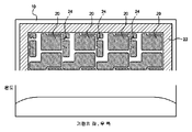
- Figure 2 is a plan view showing a conventional metal bonded ceramic substrate.
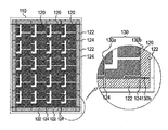
- Figure 3 is a plan view showing a metal bonded ceramic substrate according to an embodiment of the present invention.
- FIGS. 2 and 3 are views of a portion indicated by a dotted line in FIGS. 2 and 3.
- FIG. 5 is a graph schematically showing a temperature distribution during heat treatment of a conventional metal bonded ceramic substrate.
- FIG. 6 is a graph schematically showing a temperature distribution during heat treatment of a metal bonded ceramic substrate according to an embodiment of the present invention.
- FIG. 8 is a graph schematically showing the stress distribution on the upper and lower surfaces of a conventional metal bonded ceramic substrate.
- Figure 9 is a schematic diagram showing that warping occurs in a conventional metal bonded ceramic substrate.
- FIG. 10 is a plan view showing a metal bonded ceramic substrate according to another embodiment of the present invention.
- FIG. 11 is a plan view showing a metal bonded ceramic substrate according to another embodiment of the present invention.
- the configuration indicated by the reference numeral 10 will be expressed in two terms, ceramic substrate, metal bonded ceramic substrate, and the configuration indicated by the reference numeral 20 will be expressed in two terms, metal or metal layer.
- FIGS. 1A to 1F a manufacturing process of a metal bonded ceramic substrate will be described.
- the metal 20 is first placed in contact with the ceramic substrate 10 and then directly bonded (DBC).
- DBC directly bonded
- 1A is bonded by a method or an active metal method, and the bonded metal bonded ceramic substrate 10 is coated with a photosensitive film 30 called a dry film to cure only necessary portions through ultraviolet exposure (see FIG. 1B). ).
- the uncured portion of the metal layer 20 bonded and bonded to the ceramic substrate 10 is developed as shown in FIG. 1C, and the ceramic is removed through an etching process (see FIG. 1D) to remove unnecessary portions by acidic chemicals.
- a circuit pattern is formed on the substrate 10.
- the photosensitive film 30 is removed by a peeling process (see FIG. 1E), and finally a circuit pattern is formed by the metal layer 20 bonded to the ceramic substrate 10 through an etching process.
- the ceramic is melted and cut using a carbon dioxide laser or the like that generates strong light energy (see FIG. 1F).
- the metal bonded ceramic substrate 10 made by the manufacturing process described above may be designed in various arrangements according to the design method of the manufacturer or the needs of the consumer.
- the metal layer 20 may be bonded to both surfaces of the ceramic substrate 10 such that the circuit patterns are formed to be symmetrical with each other.
- the circuit pattern is formed on one surface and the metal layer 20 is not a circuit pattern on the other surface. It may be formed to occupy.
- FIG. 2 is a plan view showing a conventional metal bonded ceramic substrate
- FIG. 3 is a plan view showing a metal bonded ceramic substrate according to an embodiment of the present invention.
- FIG. 2 and 3 show a comparison between a metal bonded ceramic substrate according to the prior art and the present invention.
- a plurality of metal layers 20 are arranged in one column and one row on one surface of the ceramic substrate 10.
- all of the metal layers 20 that do not form the circuit pattern are removed.
- all unnecessary portions corresponding to the outside of the metal layer 20 are removed.
- an additional metal layer 22 is bonded to the outer side of the metal layer 20.
- the ceramic substrate 10 and the metal layer 20 may be made of various materials.
- the ceramic substrate 10 is made of ceramic materials such as alumina (Al 2 O 3 ), aluminum nitride (AlN), silicon carbide (SiC), and silicon nitride (Si 3 N 4 ), and the metal layer 20 ) Is made of copper (Cu) or aluminum (Al).
- the additional metal layer 22 is formed along the edge of the ceramic substrate 10, and may be bonded to at least one surface of the ceramic substrate 10.
- the additional metal layer 22 surrounds the outer portion of the metal layer 20 in a strap shape.
- the formed additional metal layer 22 has the advantage of improving the dimensional accuracy of the ceramic substrate 10 and reducing the temperature deviation during heat treatment to improve the bonding characteristics of the semiconductor chip. Detailed description thereof will be given below.
- cutting lines 24 are formed between the metal layers 20.
- the cutting line 24 is also formed between the metal layer 20 and the additional metal layer 22.
- the cutting lines 24 are portions formed to facilitate cutting of the metal layers 20, respectively.
- the spacing between the metal layer 20 is preferably formed equal to the spacing between the outermost metal layer 20 and the additional metal layer 22.
- the cutting line 24 is formed along a central portion between the metal layer 20 and a central portion between the outermost metal layer 20 and the additional metal layer 22.
- FIGS. 2 and 3 are views of a portion indicated by the dotted lines of FIGS. 2 and 3.
- dimension 1 the distance between the outermost metal layer 20 and the cutting line 24 is referred to as dimension 1 (L1), and the distance between the metal layer 20 and the cutting line 24 located inside is determined. Assume dimension 2 (L2).
- the metal bonded ceramic substrate 10 may be etched under the same conditions as the center portion (the portion where the metal layer is formed).
- the size of the dimension 1 and the dimension 2 may be the same, resulting in an improvement in the dimensional accuracy of the circuit pattern.
- Table 1 shows the circuit dimensions of the metal bonded ceramic substrate, and the conventional dimension 1 is about 0.1 mm larger than the dimension 2 and the dimension 1 of the present invention is almost the same as the dimension 2. This is due to the difference between the conventional metal bonded ceramic substrate which failed to equally match the environment of adjacent parts when etching the metal layer 20 and the metal bonded ceramic substrate of the present invention in which the metal layer 20 is positioned at the same distance from the adjacent parts. appear.
- FIG. 5 is a graph schematically showing a temperature distribution during heat treatment of a conventional metal bonded ceramic substrate
- FIG. 6 schematically shows a temperature distribution during heat treatment of a metal bonded ceramic substrate according to an embodiment of the present invention. The graph shown is shown.
- a solder material layer is formed on the surface of the ceramic substrate through a printing method, and the semiconductor chip is placed on the solder material layer and subjected to a bonding process.
- the temperature is maintained at 150 to 350 ° C. for about 10 to 30 minutes in a continuous heat treatment facility, the solder material layer may melt to strongly bond the semiconductor chip and the ceramic substrate 10.
- the difference in the melting degree of the brazing material layer occurs according to the deviation of the temperature received by the ceramic substrate 10 during the heat treatment.
- the temperature deviation is large, the brazing material layer does not melt, and thus the bonding is not performed normally.
- heat is concentrated, a spreading phenomenon of the brazing filler metal layer occurs and an air layer is formed therein, thereby deteriorating a bonding property.
- Table 2 shows the wettability of the brazing filler metal layer at positions (1) and (2) of FIG. 7.
- the difference between position (1) (outer part) and position (2) (middle part) is about 10%, which not only lowers the bonding characteristics with the semiconductor chip but also the process conditions. It also works against you.
- the difference in positions (1) and (2) is less than about 1%, and the average wettability is less than 5%, so that wettability can be remarkably improved compared with the prior art.
- Position 1 Position 2 Position 1 Position 2 One 21.4% 11.2% 4.2% 3.8% 2 18.5% 8.0% 3.6% 3.4% 3 19.5% 8.8% 5.4% 3.9% 4 21.2% 5.5% 4.8% 3.8% 5 18.8% 9.8% 4.2% 3.2% 6 17.5% 8.5% 4.8% 3.6% 7 19.2% 7.6% 5.5% 3.7% 8 20.1% 9.8% 4.5% 3.5% 9 20.5% 10.2% 3.8% 3.7% 10 22.6% 8.4% 4.1% 3.8% Average 19.93% 8.78% 4.49% 3.64%
- FIG. 8 a graph schematically showing stress distributions on the upper and lower surfaces of the conventional metal bonded ceramic substrate is shown in FIG. 8, and FIG. 9 is a schematic view showing that warpage occurs in the conventional metal bonded ceramic substrate.
- a semiconductor device is mounted on an upper surface of a metal bonded ceramic substrate, and various types of circuit patterns for connecting circuits and circuits, circuits, and semiconductor devices are realized through wire bonding.
- a simple pattern of a rectangular shape is formed on the lower surface without forming a complicated pattern in order to effectively radiate heat to a portion bonded to the heat sink.
- an additional metal layer 22 is further formed as described above to minimize the occurrence of such warpage.
- the area and shape of the additional metal layer 22 formed as described above the occurrence of warpage can be alleviated more, and the direction of the warpage desired can be further adjusted.
- Figure 10 is a plan view showing a metal bonded ceramic substrate according to another embodiment of the present invention
- Figure 11 is a plan view showing a metal bonded ceramic substrate according to another embodiment of the present invention.
- the same components as in the above-described embodiment are denoted by the reference numerals of 100, and detailed description thereof will be omitted.
- the additional metal layer 122 is not connected by one strap, and the cutting channel 124 is formed between the additional metal layers 122.
- the cutting channel 124 represents a portion corresponding to an extension line of the boundary of the metal layer 120.
- the cutting line 130 is composed of an inner cutting line 130a and an outer cutting line 130b.
- the outer cutting line 130b represents a cutting line located at an edge (outermost) of the metal layer 120 arranged in a plurality of columns and rows, and the inner cutting line 130a is a cutting line located inside.
- the cutting line formed between 122) is shown.
- the inner cutting line 130a does not extend to the cutting channel 124, and only the outer cutting line 130b extends to the cutting channel 124.
- the outer cutting line 130b preferably extends to the cutting channel 124 only in portions (upper and lower or left and right portions in FIG. 10) corresponding to both sides, rather than extending to the cutting channel 124. That is, at least a portion of the outer cutting line 130b extends into the cutting channel 124. This is to cut portions corresponding to both sides when cutting the additional metal layer 122, respectively, and to prevent the additional metal layer 122 positioned vertically after the cutting from being arbitrarily cut with the portion of the metal layer 120.
Landscapes
- Chemical & Material Sciences (AREA)
- Engineering & Computer Science (AREA)
- Ceramic Engineering (AREA)
- Materials Engineering (AREA)
- Structural Engineering (AREA)
- Organic Chemistry (AREA)
- Structure Of Printed Boards (AREA)
- Ceramic Products (AREA)
- Cooling Or The Like Of Semiconductors Or Solid State Devices (AREA)
Abstract
본 발명은 금속접합 세라믹기판에 관한 것이다. 본 발명은 표면에 금속층이 접합되어 회로패턴을 형성하는 세라믹기판에 관한 것이다. 회로패턴을 형성하는 금속층은 다수개가 열 및 행으로 배치된다. 그리고, 세라믹기판의 적어도 일면에는 금속층의 외곽에 위치하도록 추가 금속층이 가장자리를 따라 형성된다. 또한, 금속층 사이의 간격은 금속층과 추가 금속층 사이의 간격과 동일하게 형성됨이 바람직하다. 이와 같은 본 발명에 의하면, 본 발명에 의하면, 회로를 형성하기 위한 에칭공정 중 회로패턴의 편차를 줄여 치수 정밀도를 개선하고, 반도체 칩을 실장하기 위한 납재층 열처리 시 온도편차를 줄여 반도체 칩의 접합특성을 향상시킬 수 있으며, 금속과 세라믹의 열팽창계수 차이에 의해 발생되는 휨을 완화 또는 인위적으로 조절할 수 있는 효과가 있다.
Description
본 발명은 세라믹기판에 관한 것으로, 더욱 상세하게는 제조 시에 회로패턴의 정밀도를 개선하고 반도체 소장 실장공정의 생산성 향상과 공정효율을 높일 수 있는 구조를 가진 금속접합 세라믹기판에 관한 것이다.
종래부터 구리(Cu), 알루미늄(Al)과 같은 금속이 알루미나(Al2O3), 질화알루미늄(AlN), 탄화규소(SiC) 및 질화규소(Si3N4)와 같은 세라믹 소재의 기판에 접합된, 소위 금속접합 세라믹기판이 광범위하게 보급되어 반도체장치의 구성부품으로서 사용되고 있다.
세라믹기판과 금속회로판을 일체로 접합하는 방법으로서, 구리와 같은 금속을 세라믹기판에 접촉 배치한 후 구리의 융점(1083℃)보다는 낮고 구리 및 산소의 공융점(1065℃)보다는 높은 온도로 가열하여 구리판을 기판에 직접 접합시키는 직접접합(Direct bonding copper: DBC)방법이 개발되어 상용화되고 있으며, 최근 들어 보다 많은 열방출 및 강한 기계적인 접합물성을 유지하기 위해 금속회로기판을 납재층을 통하여 접합하는 활성 금속법에 의해 제조된 세라믹 회로기판 역시 개발되어 고신뢰성을 요구하는 전력반도체에 적용되고 있다.
상기 금속접합 세라믹기판은 최근 들어 제조 시에 대형 세라믹기판에 금속판을 접합 시킨 후 원하고자 하는 회로패턴을 인쇄회로기판의 일반적인 패턴구현방식인 화학적으로 금속을 에칭시키는 공법에 의해 구현한다. 이러한 방법은 여러 개의 배열의 회로기판을 동시에 제조할 수 있으며 최종적으로 이산화탄소 등의 레이저 가공을 통해 개별 제품으로 절단하여 사용되어진다.
하지만, 절단된 개별회로기판 중 최 외곽에 위치한 개별회로기판은 패턴의 치수가 중앙부위에 위치한 개별회로기판과 차이가 발생하며 반도체소자를 실장하기 위해 개별제품에 대해서 납재층이 인쇄된 후 열처리되는데, 이때 개별회로기판에 비해 적정 온도조건을 맞추는데 어려움이 있다. 또한, 상하부의 패턴의 유효면적 차이에 의하여 금속접합 세라믹기판은 휨이 발생하여 자동화 공정을 적용하기에 큰 문제점이 발생한다.
따라서, 본 발명의 목적은 상기한 바와 같은 종래 기술의 문제점을 해결하기 위한 것으로, 회로패턴 형성을 위한 에칭 공정 중에 치수정밀도를 개선하며 반도체소자를 실장하기 위한 납재층 인쇄 시에 유리한 휨 발생과 강도에 대한 개선을 통한 안정적인 공정진행과 납재층의 열처리 시에 온도 균일성을 유지하는데 효과적인 복합배열 구조를 가진 금속접합 세라믹기판을 제공하기 위한 것이다.
본 발명이 이루고자 하는 기술적 과제들은 이상에서 언급한 기술적 과제들로 제한되지 않으며, 언급되지 않은 또 다른 기술적 과제들은 아래의 기재로부터 본 발명이 속하는 기술분야에서 통상의 지식을 가진 자에게 명확하게 이해될 수 있을 것이다.
상기한 바와 같은 목적을 달성하기 위한 본 발명의 특징에 따르면, 본 발명은 표면에 금속층이 접합되어 회로패턴을 형성하고, 상기 금속층은 다수개가 열 및 행으로 배치되는 금속접합 세라믹기판에 있어서, 상기 세라믹기판의 적어도 일면에는 상기 금속층의 외곽에 위치하도록 추가 금속층이 가장자리를 따라 형성됨을 특징으로 한다.
상기 금속층 사이의 간격은 최외곽에 위치한 금속층과 추가 금속층 사이의 간격과 동일하게 형성됨을 특징으로 한다.
상기 금속층의 사이 및 상기 금속층과 추가 금속층의 사이에는 적어도 하나 이상의 절단 라인이 형성됨을 특징으로 한다.
상기 절단 라인은 상기 금속층이 가장자리에 형성된 외부 절단 라인과 상기 금속층의 사이에 형성된 내부 절단 라인으로 구성됨을 특징으로 한다.
상기 추가 금속층에는 다수개가 열 및 행으로 배치되는 상기 금속층의 경계의 연장선에 해당하는 부분에 절단 채널이 형성됨을 특징으로 한다.
상기 내부 절단 라인은 상기 금속층의 가장자리까지만 연장되고, 상기 외부 절단 라인은 상기 절단 채널을 통해 세라믹기판의 가장자리까지 연장됨을 특징으로 한다.
상기 외부 절단 라인 및 내부 절단 라인은 상기 절단 채널을 통해 세라믹기판의 가장자리까지 연장됨을 특징으로 한다.
상기 세라믹기판은 알루미나(Al2O3), 질화알루미늄(AlN), 탄화규소(SiC) 또는 질화규소(Si3N4)의 세라믹소재로 만들어지고, 상기 금속층(20)은 구리 또는 알루미늄으로 만들어짐을 특징으로 한다.
상기 추가 금속층은 상기 세라믹기판의 상면 및 하면에 각각 다른 면적과 형상을 가지도록 형성됨을 특징으로 한다.
본 발명에 의하면, 회로를 형성하기 위한 에칭공정 중 회로패턴의 편차를 줄여 치수 정밀도를 개선하고, 반도체 칩을 실장하기 위한 납재층 열처리 시 온도편차를 줄여 반도체 칩의 접합특성을 향상시킬 수 있으며, 금속과 세라믹의 열팽창계수 차이에 의해 발생되는 휨을 완화 또는 인위적으로 조절할 수 있는 효과가 있다.
도 1a 내지 도 1f는 금속접합 세라믹기판의 제조 공정을 개략적으로 보인 모식도.
도 2는 종래의 금속접합 세라믹기판을 보인 평면도.
도 3은 본 발명의 일 실시예에 따른 금속접합 세라믹기판을 보인 평면도.
도 4는 도 2 및 도 3의 점선으로 표시한 부분의 확대도.
도 5는 종래의 금속접합 세라믹기판의 열처리 시 온도분포를 개략적으로 보인 그래프.
도 6은 본 발명의 일 실시예에 따른 금속접합 세라믹기판의 열처리 시 온도분포를 개략적으로 보인 그래프.
도 7은 금속접합 세라믹기판의 납재층 열처리 후의 엑스레이 사진.
도 8은 종래의 금속접합 세라믹기판의 상면과 하면의 응력분포를 개략적으로 보인 그래프.
도 9는 종래의 금속접합 세라믹기판에서 휨이 발생한 것을 보인 모식도.
도 10은 본 발명의 다른 실시예에 따른 금속접합 세라믹기판을 보인 평면도.
도 11은 본 발명의 또 다른 실시예에 따른 금속접합 세라믹기판을 보인 평면도.
이하에서는 본 발명에 의한 금속접합 세라믹기판의 일 실시예를 첨부된 도면을 참고하여 상세하게 설명한다.
설명에 앞서 이하에서 도면부호 10으로 표시된 구성은 세라믹기판, 금속접합 세라믹기판의 두 가지 용어로 표현하며, 도면부호 20으로 표시된 구성은 금속 또는 금속층의 두 가지 용어로 표현하도록 한다.
먼저, 도 1a 내지 도 1f를 참조하여 금속접합 세라믹기판의 제조 공정을 살펴보면, 일반적인 금속접합 세라믹기판의 제조 공정에서는 최초에 금속(20)을 세라믹기판(10)에 접촉 배치한 후에 직접접합(DBC) 방법 또는 활성 금속법에 의해 도 1a와 같이 접합이 되고, 접합이 된 금속접합 세라믹기판(10)을 드라이 필름이라는 감광성 필름(30)을 입혀 자외선 노광을 통해 필요한 부분만을 경화시킨다(도 1b 참조).
다음으로, 상기 세라믹기판(10)에 접합되어 형성된 금속층(20)에서 경화되지 않은 부분을 도 1c와 같이 현상을 하고, 산성약품에 의해 불필요한 부분을 제거하는 에칭공정(도 1d 참조)을 통해 세라믹기판(10)에 회로패턴을 형성한다. 그리고, 상기 감광성 필름(30)은 박리공정(도 1e 참조)에 의해 제거되고, 최종적으로 회로패턴은 에칭공정을 통해 세라믹기판(10)에 접합된 금속층(20)에 의해 형성된다.
최종적으로, 세라믹기판(10)에 일정한 형태로 배치된 회로패턴을 개별적으로 절단하기 위해 강한 광 에너지를 발생시키는 이산화탄소 레이저 등을 사용하여 세라믹을 녹여 절단(도 1f 참조)을 하게 된다. 이상에서 설명한 제조 공정에 의해 만들어진 금속접합 세라믹기판(10)은 제조자의 설계방법 또는 수요자의 요구에 따라 다양한 배열로 설계될 수 있다.
예를 들어, 세라믹기판(10)의 양면에 서로 대칭되도록 회로패턴이 형성되도록 금속층(20)을 접합할 수도 있고, 일면에는 회로패턴이 형성되고 타면에는 회로패턴이 아닌 금속층(20)이 전체를 차지하도록 형성될 수도 있다.
다음으로, 도 2에는 종래의 금속접합 세라믹기판을 보인 평면도가 도시되어 있고, 도 3에는 본 발명의 일 실시예에 따른 금속접합 세라믹기판을 보인 평면도가 도시되어 있다.
이를 참조하면, 도 2 및 도 3은 종래와 본 발명에 의한 금속접합 세라믹기판을 비교한 것을 보인 것이다. 종래에는 세라믹기판(10)의 일면에 다수개의 금속층(20)이 열 및 행으로 배치되어 있는 것을 알 수 있다. 여기에서 회로패턴을 형성하지 않는 금속층(20)은 모두 제거된다. 즉, 상기 금속층(20)의 외곽에 해당하는 불필요한 부분은 모두 제거된다. 하지만, 도 3을 참조하면, 본 발명에 의한 금속접합 세라믹기판에서는 금속층(20)의 외곽에 추가 금속층(22)이 접합되어 구비된다.
상기 세라믹기판(10) 및 금속층(20)은 다양한 소재로 만들어질 수 있다. 예를 들어, 상기 세라믹기판(10)은 알루미나(Al2O3), 질화알루미늄(AlN), 탄화규소(SiC) 및 질화규소(Si3N4) 등의 세라믹소재로 만들어지고, 상기 금속층(20)은 구리(Cu) 또는 알루미늄(Al)으로 만들어진다.
상기 추가 금속층(22)은 상기 세라믹기판(10)의 가장자리를 따라 형성되는 것으로서, 세라믹기판(10)의 적어도 일면에 접합되어 형성될 수 있다. 상기 추가 금속층(22)은 스트랩 형상으로 금속층(20)의 외곽을 감싸게 된다. 이와 같은 형성된 추가 금속층(22)은 세라믹기판(10)의 치수 정밀도를 개선하고 열처리 시 온도편차를 줄여 반도체 칩의 접합특성을 향상시킬 수 있는 이점이 있다. 이에 대한 구체적인 설명은 이하에서 하기로 한다.
한편, 상기 금속층(20)의 사이에는 각각 절단 라인(24)이 형성되어 있다. 또한, 상기 절단 라인(24)은 금속층(20)과 추가 금속층(22)의 사이에도 형성된다. 상기 절단 라인(24)은 금속층(20)을 각각 절단하기 쉽게 하기 위해 형성된 부분이다.
본 실시예에서 세라믹기판(10)의 치수 정밀도를 개선하기 위해 상기 금속층(20) 사이의 간격은 최외곽에 위치한 금속층(20)과 추가 금속층(22) 사이의 간격과 동일하게 형성됨이 바람직하다. 그리고, 상기 금속층(20) 사이의 중앙부와, 최외곽에 위치한 금속층(20)과 추가 금속층(22) 사이의 중앙부를 따라 상기 절단 라인(24)이 형성된다.
도 4에는 도 2 및 도 3의 점선으로 표시한 부분의 확대도가 도시되어 있다.
이를 참조하면, 도 4에서 가장 외곽에 위치한 금속층(20)과 절단 라인(24) 사이의 간격을 치수 1(L1)이라 하고, 내측에 위치한 금속층(20)과 절단 라인(24) 사이의 간격을 치수 2(L2)라 가정한다.
금속접합 세라믹기판(10)에서 회로패턴의 정밀도가 매우 중요하기 때문에 과거에는 회로패턴의 형상을 금형으로 프레싱하여 단일기판에 직접 접합하여 제조하였지만, 최근에는 도 1에서 언급하였듯이 에칭공법을 적용하여 원하고자 하는 회로패턴 만을 남겨두고 나머지 불필요한 부분을 화학적인 반응을 통해 제거한다. 이때 종래의 금속접합 세라믹기판(10, 도 2)은 최외곽에 추가 금속층(22)이 형성되어 있지 않으므로, 가운데 부분(금속층이 형성된 부분)보다 에칭의 진행 속도가 빨라 치수 1은 치수 2보다 항상 크게 나타나는 문제가 있었다.
하지만, 본 발명에 의한 금속접합 세라믹기판(10, 도 3)에서는 최외곽에 추가 금속층(22)이 형성되어 있으므로 가운데 부분(금속층이 형성된 부분)과 동일한 조건으로 에칭이 될 수 있다. 이와 같이 본 발명에 의한 금속접합 세라믹기판(10)에서는 치수 1과 치수 2의 크기가 동일하게 나타날 수 있게 되므로 회로패턴의 치수 정밀도가 향상되는 결과를 가져온다.
하기 [표 1]은 금속접합 세라믹기판의 회로치수를 나타낸 것으로서, 종래의 치수 1은 치수 2에 비해서 약 0.1mm가 크고 본 발명의 치수 1은 치수 2와 거의 동일하게 나타난다. 이는 금속층(20)을 에칭 시 상호 인접한 부위의 환경을 동일하게 맞추지 못한 종래의 금속접합 세라믹기판과, 상호 인접한 부위에 동일한 거리에 금속층(20)을 위치시킨 본 발명의 금속접합 세라믹기판의 차이로부터 나타난다.
표 1
| 번호 | 종래 | 본 발명 | ||
| 치수1 | 치수2 | 치수1 | 치수2 | |
| 설계값 | 0.6 | 0.6 | 0.6 | 0.6 |
| 1 | 0.702 | 0.613 | 0.608 | 0.611 |
| 2 | 0.712 | 0.610 | 0.604 | 0.608 |
| 3 | 0.708 | 0.621 | 0.602 | 0.620 |
| 4 | 0.692 | 0.619 | 0.609 | 0.622 |
| 5 | 0.699 | 0.601 | 0.611 | 0.601 |
| 6 | 0.705 | 0.602 | 0.622 | 0.598 |
| 7 | 0.712 | 0.605 | 0.611 | 0.621 |
| 8 | 0.705 | 0.607 | 0.617 | 0.609 |
| 9 | 0.704 | 0.611 | 0.611 | 0.611 |
| 10 | 0.698 | 0.605 | 0.608 | 0.624 |
| 평균 | 0.704 | 0.609 | 0.610 | 0.613 |
다음으로, 도 5에는 종래의 금속접합 세라믹기판의 열처리 시 온도분포를 개략적으로 보인 그래프가 도시되어 있고, 도 6에는 본 발명의 일 실시예에 따른 금속접합 세라믹기판의 열처리 시 온도분포를 개략적으로 보인 그래프가 도시되어 있다.
이를 참조하면, 금속접합 세라믹기판 위에 반도체 칩을 실장하기 위해서 납재층이 세라믹기판의 표면에 인쇄방법을 통해 형성되며, 납재층 위에 반도체 칩을 위치시키고 이를 접합시키는 공정을 거치게 된다. 이때 연속적인 열처리 설비에서 약 10 내지 30분 정도에서 150 내지 350℃ 에서 온도을 유지시키면 납재층이 녹아서 반도체 칩과 세라믹기판(10)이 강하게 접합될 수 있다.
여기에서, 열처리 시 세라믹기판(10)이 받는 온도의 편차에 따라서 납재층의 녹는 정도의 차이가 발생하게 되는데, 온도편차가 크게 나타날 경우에는 납재층이 녹지 않아 접합이 정상적으로 이루어지지 않으며, 과도하게 열이 집중될 경우에는 납재층의 번짐 현상이 발생하고 내부에 공기층이 형성되어 접합특성이 떨어지는 문제가 있다.
도 5를 참조하면, 종래의 금속접합 세라믹기판에서는 가장자리 영역에 추가 금속층(22)이 형성되지 않으므로, 단일 기판 내에서 온도분포 차이가 발생하여 열처리 시 상기한 바와 같이 납재층의 접합특성이 떨어지는 문제가 있다.
반면에 도 6을 참조하면, 본 발명에 의한 금속접합 세라믹기판에서는 가장자리 영역에 추가 금속층(22)이 형성되므로, 세라믹기판(10)의 폭방향으로 온도분포가 비교적 균등하게 나타난다. 따라서, 열처리 시 납재층의 녹는 정도가 고르게 되어 납재층의 접합특성이 향상되고 열처리 특성이 개선되는 이점이 있다.
도 7을 참조하면, 종래와 같이 온도분포 차이가 발생할 때 실제 납재층의 접합면적을 엑스레이(X-ray)로 촬영한 것으로서, 미접합된 부위와 내부 공기층(void)이 형성되어 있는 것을 확인할 수 있다.
하기 [표 2]는 도 7의 (1)번 위치와 (2)번 위치에서의 납재층의 젖음성을 보인 것이다. 이를 참조하면, 종래의 경우에는 (1)번 위치(외곽부분)와 (2)번 위치(중간부분)의 차이가 약 10% 정도로 나타나며 이는 반도체 칩과의 접합특성을 현저하게 낮출뿐만 아니라 공정 조건을 선정하는 데에도 불리하게 작용한다. 반면에, 본 발명에서는 (1)번과 (2)번 위치에서의 차이가 대략 1% 미만이고, 젖음성의 평균치가 5% 미만이어서 젖음성이 종래에 비해 현저하게 개선될 수 있다.
표 2
| 번호 | 종래 | 본 발명 | ||
| 1번 위치 | 2번 위치 | 1번 위치 | 2번 위치 | |
| 1 | 21.4% | 11.2% | 4.2% | 3.8% |
| 2 | 18.5% | 8.0% | 3.6% | 3.4% |
| 3 | 19.5% | 8.8% | 5.4% | 3.9% |
| 4 | 21.2% | 5.5% | 4.8% | 3.8% |
| 5 | 18.8% | 9.8% | 4.2% | 3.2% |
| 6 | 17.5% | 8.5% | 4.8% | 3.6% |
| 7 | 19.2% | 7.6% | 5.5% | 3.7% |
| 8 | 20.1% | 9.8% | 4.5% | 3.5% |
| 9 | 20.5% | 10.2% | 3.8% | 3.7% |
| 10 | 22.6% | 8.4% | 4.1% | 3.8% |
| 평균 | 19.93% | 8.78% | 4.49% | 3.64% |
다음으로, 도 8에는 종래의 금속접합 세라믹기판의 상면과 하면의 응력분포를 개략적으로 보인 그래프가 도시되어 있고, 도 9에는 종래의 금속접합 세라믹기판에서 휨이 발생한 것을 보인 모식도가 도시되어 있다.
일반적으로 금속접합 세라믹기판의 상면에는 반도체 소자가 실장되고 와이어 본딩(Wire bonding)을 통해 회로와 회로, 회로와 반도체 소자를 연결해주기 위한 다양한 형태의 회로패턴이 구현된다. 반면에, 하면에는 방열판과 접합되는 부위로 방열을 효과적으로 이루기 위해 복잡한 패턴을 형성하지 않고 직사각형 모양의 단순한 패턴이 형성된다.
도 8을 참조하면, 종래의 금속접합 세라믹기판에서는 상면과 하면에서는 구리(약 16.7×10⁻⁶/℃)와 세라믹(AIN: 4.6×10⁻⁶/℃, Alumina: 6.8×10⁻⁶/℃)의 큰 열팽창계수의 차이에 의해 응력분포가 다르게 나타난다. 즉, 회로패턴이 다양하게 형성된 상면의 경우에는 응력이 완화되어 있으며 하면의 경우에는 회로패턴의 끊김이 없어 큰 응력이 전반적으로 발생함을 알 수 있다.
이와 같은 응력분포에 의해 종래의 금속접합 세라믹기판에서는 도 9에서와 같이 휨이 발생하게 된다. 본 발명에서는 이러한 휨의 발생을 최소화하기 위해 상술한 바와 같이 추가 금속층(22)이 더 형성되어 있다. 이와 같이 형성된 추가 금속층(22)의 면적 및 형상을 다양하게 함으로써 휨의 발생을 보다 완화시킬 수 있고, 더 나아가 원하고자 하는 휨의 방향을 조절할 수 있게 된다.
한편, 도 10에는 본 발명의 다른 실시예에 따른 금속접합 세라믹기판을 보인 평면도가 도시되어 있고, 도 11에는 본 발명의 또 다른 실시예에 따른 금속접합 세라믹기판을 보인 평면도가 도시되어 있다. 본 도면에서 상술한 실시예와 동일한 구성요소에 대해서는 백번 대의 도면부호를 부여하고 이에 대한 자세한 설명은 생략하기로 한다.
먼저, 도 10을 참조하면, 상술한 실시예와 달리, 추가 금속층(122)이 하나의 스트랩으로 연결되어 있지 않고 추가 금속층(122)의 사이에 절단 채널(124)이 형성된다. 상기 절단 채널(124)은 상기 금속층(120)의 경계의 연장선에 해당하는 부분을 나타낸다.
상기 절단 라인(130)은 내부 절단 라인(130a)과 외부 절단 라인(130b)으로 구성된다. 상기 외부 절단 라인(130b)은 다수개의 열 및 행으로 배치된 금속층(120)의 가장자리(최외곽)에 위치한 절단 라인을 나타내고, 상기 내부 절단 라인(130a)은 내측에 위치한 절단 라인으로서 상기 금속층(122)의 사이에 형성된 절단 라인을 나타낸다.
도 10에 도시된 실시예에서는 상기 내부 절단 라인(130a)은 상기 절단 채널(124)로 연장되지 않고, 외부 절단 라인(130b)만 절단 채널(124)로 연장되도록 형성된다. 여기에서, 상기 외부 절단 라인(130b)은 모두 절단 채널(124)로 연장되는 것보다는 양측에 해당하는 부분(도 10에서 상하부분 또는 좌우부분)만 절단 채널(124)로 연장되는 것이 바람직하다. 즉, 상기 외부 절단 라인(130b) 중에 적어도 일부가 절단 채널(124)로 연장된다. 이는 상기 추가 금속층(122)을 각각 절단할 때 양측에 해당하는 부분을 먼저 절단하고, 절단 후에도 수직하게 위치한 추가 금속층(122)이 금속층(120) 부분과 임의로 절단되지 않도록 하기 위함이다.
다음으로, 도 11에 도시된 실시예에서는 외부 절단 라인(130b)뿐만 아니라 내부 절단 라인(130a) 모두가 상기 절단 채널(124)을 통해 상기 세라믹기판(110)의 가장자리까지 연장된다.
본 발명의 권리범위는 위에서 설명된 실시예에 한정되지 않고 청구범위에 기재된 바에 의해 정의되며, 본 발명의 기술분야에서 통상의 지식을 가진 자가 청구범위에 기재된 권리범위 내에서 다양한 변형과 개작을 할 수 있다는 것은 자명하다.
Claims (9)
- 표면에 금속층이 접합되어 회로패턴을 형성하고, 상기 금속층은 다수개가 열 및 행으로 배치되는 금속접합 세라믹기판에 있어서,상기 세라믹기판의 적어도 일면에는 상기 금속층의 외곽에 위치하도록 추가 금속층이 가장자리를 따라 형성됨을 특징으로 하는 금속접합 세라믹기판.
- 제 1 항에 있어서,상기 금속층 사이의 간격은 최외곽에 위치한 금속층과 추가 금속층 사이의 간격과 동일하게 형성됨을 특징으로 하는 금속접합 세라믹기판.
- 제 1 항에 있어서,상기 금속층의 사이 및 상기 금속층과 추가 금속층의 사이에는 적어도 하나 이상의 절단 라인이 형성됨을 특징으로 하는 금속접합 세라믹기판.
- 제 3 항에 있어서,상기 절단 라인은 상기 금속층이 가장자리에 형성된 외부 절단 라인과 상기 금속층의 사이에 형성된 내부 절단 라인으로 구성됨을 특징으로 하는 금속접합 세라믹기판.
- 제 4 항에 있어서,상기 추가 금속층에는 다수개가 열 및 행으로 배치되는 상기 금속층의 경계의 연장선에 해당하는 부분에 절단 채널이 형성됨을 특징으로 하는 금속접합 세라믹기판.
- 제 5 항에 있어서,상기 내부 절단 라인은 상기 금속층의 가장자리까지만 연장되고, 상기 외부 절단 라인은 상기 절단 채널을 통해 세라믹기판의 가장자리까지 연장됨을 특징으로 하는 금속접합 세라믹기판.
- 제 5 항에 있어서,상기 외부 절단 라인 및 내부 절단 라인은 상기 절단 채널을 통해 세라믹기판의 가장자리까지 연장됨을 특징으로 하는 금속접합 세라믹기판.
- 제 1 항에 있어서,상기 세라믹기판은 알루미나(Al2O3), 질화알루미늄(AlN), 탄화규소(SiC) 또는 질화규소(Si3N4)의 세라믹소재로 만들어지고, 상기 금속층(20)은 구리 또는 알루미늄으로 만들어짐을 특징으로 하는 금속접합 세라믹기판.
- 제 1 항에 있어서,상기 추가 금속층은 상기 세라믹기판의 상면 및 하면에 각각 다른 면적과 형상을 가지도록 형성됨을 특징으로 하는 금속접합 세라믹기판.
Priority Applications (2)
| Application Number | Priority Date | Filing Date | Title |
|---|---|---|---|
| EP11753594.8A EP2546870A4 (en) | 2010-03-09 | 2011-03-09 | Metal-bonded ceramic substrate |
| JP2012556974A JP5642808B2 (ja) | 2010-03-09 | 2011-03-09 | 金属接合セラミック基板 |
Applications Claiming Priority (2)
| Application Number | Priority Date | Filing Date | Title |
|---|---|---|---|
| KR10-2010-0020879 | 2010-03-09 | ||
| KR1020100020879A KR101675727B1 (ko) | 2010-03-09 | 2010-03-09 | 금속접합 세라믹기판 |
Publications (2)
| Publication Number | Publication Date |
|---|---|
| WO2011111989A2 true WO2011111989A2 (ko) | 2011-09-15 |
| WO2011111989A3 WO2011111989A3 (ko) | 2012-01-05 |
Family
ID=44563992
Family Applications (1)
| Application Number | Title | Priority Date | Filing Date |
|---|---|---|---|
| PCT/KR2011/001609 Ceased WO2011111989A2 (ko) | 2010-03-09 | 2011-03-09 | 금속접합 세라믹기판 |
Country Status (4)
| Country | Link |
|---|---|
| EP (1) | EP2546870A4 (ko) |
| JP (1) | JP5642808B2 (ko) |
| KR (1) | KR101675727B1 (ko) |
| WO (1) | WO2011111989A2 (ko) |
Cited By (5)
| Publication number | Priority date | Publication date | Assignee | Title |
|---|---|---|---|---|
| US20160192476A1 (en) * | 2014-12-29 | 2016-06-30 | Kcc Corporation | Warpage-preventing structure of substrate |
| CN108059485A (zh) * | 2017-12-05 | 2018-05-22 | 天津荣事顺发电子有限公司 | 一种微型超薄氮化铝陶瓷电路板及制备方法 |
| WO2020222501A1 (ko) * | 2019-05-02 | 2020-11-05 | 주식회사 아모센스 | 세라믹 기판 및 그의 제조방법 |
| CN113614261A (zh) * | 2019-03-25 | 2021-11-05 | 京瓷株式会社 | 电路衬底及具备它的散热衬底或电子设备 |
| CN113764292A (zh) * | 2021-11-08 | 2021-12-07 | 上海曦智科技有限公司 | 半导体装置及其制造方法 |
Families Citing this family (4)
| Publication number | Priority date | Publication date | Assignee | Title |
|---|---|---|---|---|
| JP2719412B2 (ja) | 1989-08-02 | 1998-02-25 | 三洋電機株式会社 | 赤外線制御装置 |
| CN112189382A (zh) * | 2018-05-23 | 2021-01-05 | 住友电木株式会社 | 电路基板的制造方法 |
| KR102244833B1 (ko) | 2019-12-10 | 2021-04-27 | 주식회사 유텔 | 적층형 lcp 전자소자 |
| CN117116775B (zh) * | 2023-09-25 | 2024-03-26 | 江苏富乐华半导体科技股份有限公司 | 一种厚金属层陶瓷基板的图形设计方法 |
Family Cites Families (8)
| Publication number | Priority date | Publication date | Assignee | Title |
|---|---|---|---|---|
| DE69021438T2 (de) * | 1989-05-16 | 1996-01-25 | Marconi Gec Ltd | Verfahren zur Herstellung einer Flip-Chip-Lötstruktur für Anordnungen mit Gold-Metallisierung. |
| JP2876989B2 (ja) * | 1994-05-31 | 1999-03-31 | 松下電工株式会社 | プリント配線板の製造方法 |
| JP4077888B2 (ja) * | 1995-07-21 | 2008-04-23 | 株式会社東芝 | セラミックス回路基板 |
| EP0935286A4 (en) * | 1997-05-26 | 2008-04-09 | Sumitomo Electric Industries | COPPER CIRCUIT CONNECTING SUBSTRATE AND ITS MANUFACTURE |
| JP4168114B2 (ja) * | 2001-09-28 | 2008-10-22 | Dowaホールディングス株式会社 | 金属−セラミックス接合体 |
| JP2007019123A (ja) * | 2005-07-06 | 2007-01-25 | Sumitomo Metal Electronics Devices Inc | セラミック回路基板集合体 |
| JP3993619B2 (ja) * | 2005-07-06 | 2007-10-17 | 株式会社住友金属エレクトロデバイス | セラミック回路基板集合体 |
| JP2007324277A (ja) * | 2006-05-31 | 2007-12-13 | Sumitomo Metal Electronics Devices Inc | セラミック回路基板集合体 |
-
2010
- 2010-03-09 KR KR1020100020879A patent/KR101675727B1/ko active Active
-
2011
- 2011-03-09 JP JP2012556974A patent/JP5642808B2/ja active Active
- 2011-03-09 WO PCT/KR2011/001609 patent/WO2011111989A2/ko not_active Ceased
- 2011-03-09 EP EP11753594.8A patent/EP2546870A4/en not_active Withdrawn
Non-Patent Citations (2)
| Title |
|---|
| None |
| See also references of EP2546870A4 |
Cited By (10)
| Publication number | Priority date | Publication date | Assignee | Title |
|---|---|---|---|---|
| US20160192476A1 (en) * | 2014-12-29 | 2016-06-30 | Kcc Corporation | Warpage-preventing structure of substrate |
| US9839120B2 (en) * | 2014-12-29 | 2017-12-05 | Kcc Corporation | Warpage-preventing structure of substrate |
| CN108059485A (zh) * | 2017-12-05 | 2018-05-22 | 天津荣事顺发电子有限公司 | 一种微型超薄氮化铝陶瓷电路板及制备方法 |
| CN108059485B (zh) * | 2017-12-05 | 2023-06-13 | 上海铠琪科技有限公司 | 一种微型超薄氮化铝陶瓷电路板及制备方法 |
| CN113614261A (zh) * | 2019-03-25 | 2021-11-05 | 京瓷株式会社 | 电路衬底及具备它的散热衬底或电子设备 |
| WO2020222501A1 (ko) * | 2019-05-02 | 2020-11-05 | 주식회사 아모센스 | 세라믹 기판 및 그의 제조방법 |
| US20220208697A1 (en) * | 2019-05-02 | 2022-06-30 | Amosense Co., Ltd. | Ceramic substrate and manufacturing method therefor |
| US12183689B2 (en) * | 2019-05-02 | 2024-12-31 | Amosense Co., Ltd. | Ceramic substrate and manufacturing method therefor |
| CN113764292A (zh) * | 2021-11-08 | 2021-12-07 | 上海曦智科技有限公司 | 半导体装置及其制造方法 |
| CN113764292B (zh) * | 2021-11-08 | 2022-03-01 | 上海曦智科技有限公司 | 半导体装置及其制造方法 |
Also Published As
| Publication number | Publication date |
|---|---|
| KR20110101692A (ko) | 2011-09-16 |
| WO2011111989A3 (ko) | 2012-01-05 |
| JP5642808B2 (ja) | 2014-12-17 |
| KR101675727B1 (ko) | 2016-11-14 |
| JP2013522872A (ja) | 2013-06-13 |
| EP2546870A2 (en) | 2013-01-16 |
| EP2546870A4 (en) | 2017-11-29 |
Similar Documents
| Publication | Publication Date | Title |
|---|---|---|
| WO2011111989A2 (ko) | 금속접합 세라믹기판 | |
| US5616958A (en) | Electronic package | |
| JP2976917B2 (ja) | 半導体装置 | |
| CN102132403B (zh) | 模制超薄半导体管芯封装和使用该封装的系统及其制造方法 | |
| CN1205548A (zh) | 用于引线连接式芯片的有机芯片载体 | |
| CN103828079B (zh) | 承载设备、具有承载设备的电气设备和其制造方法 | |
| US11676882B2 (en) | Method of manufacturing power module substrate board and ceramic-copper bonded body | |
| WO2023163439A1 (ko) | 세라믹 기판 유닛 및 그 제조방법 | |
| WO2014051233A2 (en) | Printed circuit board | |
| WO2023163438A1 (ko) | 세라믹 기판 유닛 및 그 제조방법 | |
| WO2022203288A1 (ko) | 파워모듈 및 그 제조방법 | |
| KR101733442B1 (ko) | 기판의 휨 방지 구조체 | |
| WO2024063410A1 (ko) | 히트싱크 일체형 파워모듈용 기판 및 그 제조방법 | |
| WO2017155249A1 (ko) | 세라믹 기판 제조용 적층 시스템 및 이를 이용한 세라믹 기판의 제조 방법 | |
| WO2016028098A1 (ko) | 메탈 코어 인쇄회로기판 및 그 제조 방법 | |
| WO2020149587A1 (ko) | 방열판재 | |
| KR102923480B1 (ko) | 세라믹 기판 유닛 및 그 제조방법 | |
| KR102855285B1 (ko) | 세라믹 기판 유닛 및 그 제조방법 | |
| TWI851015B (zh) | 內埋陶瓷基板之電路板結構及其製程 | |
| JP4641635B2 (ja) | ヒートシンク集合体 | |
| JP2000082762A (ja) | 半導体装置 | |
| WO2024136625A1 (ko) | 전자 패키지 및 전자 패키지 제조방법 | |
| WO2024210582A2 (ko) | 다층 금속접합 세라믹 기판 및 그 제조방법 | |
| JPS5931091A (ja) | 混成集積回路装置 | |
| JP2022149755A (ja) | 多数個取り基板及び配線基板並びに電子部品 |
Legal Events
| Date | Code | Title | Description |
|---|---|---|---|
| 121 | Ep: the epo has been informed by wipo that ep was designated in this application |
Ref document number: 11753594 Country of ref document: EP Kind code of ref document: A2 |
|
| WWE | Wipo information: entry into national phase |
Ref document number: 2012556974 Country of ref document: JP |
|
| NENP | Non-entry into the national phase |
Ref country code: DE |
|
| WWE | Wipo information: entry into national phase |
Ref document number: 2011753594 Country of ref document: EP |