WO2012104902A1 - Dispositif à semi-conducteurs et son procédé de fabrication - Google Patents
Dispositif à semi-conducteurs et son procédé de fabrication Download PDFInfo
- Publication number
- WO2012104902A1 WO2012104902A1 PCT/JP2011/000530 JP2011000530W WO2012104902A1 WO 2012104902 A1 WO2012104902 A1 WO 2012104902A1 JP 2011000530 W JP2011000530 W JP 2011000530W WO 2012104902 A1 WO2012104902 A1 WO 2012104902A1
- Authority
- WO
- WIPO (PCT)
- Prior art keywords
- semiconductor device
- gate electrode
- film
- substrate
- less
- Prior art date
- Legal status (The legal status is an assumption and is not a legal conclusion. Google has not performed a legal analysis and makes no representation as to the accuracy of the status listed.)
- Ceased
Links
Images



Classifications
-
- H—ELECTRICITY
- H10—SEMICONDUCTOR DEVICES; ELECTRIC SOLID-STATE DEVICES NOT OTHERWISE PROVIDED FOR
- H10D—INORGANIC ELECTRIC SEMICONDUCTOR DEVICES
- H10D64/00—Electrodes of devices having potential barriers
- H10D64/20—Electrodes characterised by their shapes, relative sizes or dispositions
- H10D64/27—Electrodes not carrying the current to be rectified, amplified, oscillated or switched, e.g. gates
- H10D64/311—Gate electrodes for field-effect devices
- H10D64/411—Gate electrodes for field-effect devices for FETs
- H10D64/511—Gate electrodes for field-effect devices for FETs for IGFETs
- H10D64/514—Gate electrodes for field-effect devices for FETs for IGFETs characterised by the insulating layers
-
- H—ELECTRICITY
- H10—SEMICONDUCTOR DEVICES; ELECTRIC SOLID-STATE DEVICES NOT OTHERWISE PROVIDED FOR
- H10D—INORGANIC ELECTRIC SEMICONDUCTOR DEVICES
- H10D30/00—Field-effect transistors [FET]
- H10D30/01—Manufacture or treatment
- H10D30/021—Manufacture or treatment of FETs having insulated gates [IGFET]
- H10D30/031—Manufacture or treatment of FETs having insulated gates [IGFET] of thin-film transistors [TFT]
- H10D30/0312—Manufacture or treatment of FETs having insulated gates [IGFET] of thin-film transistors [TFT] characterised by the gate electrodes
- H10D30/0316—Manufacture or treatment of FETs having insulated gates [IGFET] of thin-film transistors [TFT] characterised by the gate electrodes of lateral bottom-gate TFTs comprising only a single gate
-
- H—ELECTRICITY
- H10—SEMICONDUCTOR DEVICES; ELECTRIC SOLID-STATE DEVICES NOT OTHERWISE PROVIDED FOR
- H10D—INORGANIC ELECTRIC SEMICONDUCTOR DEVICES
- H10D30/00—Field-effect transistors [FET]
- H10D30/01—Manufacture or treatment
- H10D30/021—Manufacture or treatment of FETs having insulated gates [IGFET]
- H10D30/031—Manufacture or treatment of FETs having insulated gates [IGFET] of thin-film transistors [TFT]
- H10D30/0321—Manufacture or treatment of FETs having insulated gates [IGFET] of thin-film transistors [TFT] comprising silicon, e.g. amorphous silicon or polysilicon
-
- H—ELECTRICITY
- H10—SEMICONDUCTOR DEVICES; ELECTRIC SOLID-STATE DEVICES NOT OTHERWISE PROVIDED FOR
- H10D—INORGANIC ELECTRIC SEMICONDUCTOR DEVICES
- H10D30/00—Field-effect transistors [FET]
- H10D30/60—Insulated-gate field-effect transistors [IGFET]
- H10D30/67—Thin-film transistors [TFT]
- H10D30/6729—Thin-film transistors [TFT] characterised by the electrodes
- H10D30/673—Thin-film transistors [TFT] characterised by the electrodes characterised by the shapes, relative sizes or dispositions of the gate electrodes
-
- H—ELECTRICITY
- H10—SEMICONDUCTOR DEVICES; ELECTRIC SOLID-STATE DEVICES NOT OTHERWISE PROVIDED FOR
- H10D—INORGANIC ELECTRIC SEMICONDUCTOR DEVICES
- H10D30/00—Field-effect transistors [FET]
- H10D30/60—Insulated-gate field-effect transistors [IGFET]
- H10D30/67—Thin-film transistors [TFT]
- H10D30/6729—Thin-film transistors [TFT] characterised by the electrodes
- H10D30/6737—Thin-film transistors [TFT] characterised by the electrodes characterised by the electrode materials
- H10D30/6739—Conductor-insulator-semiconductor electrodes
-
- H—ELECTRICITY
- H10—SEMICONDUCTOR DEVICES; ELECTRIC SOLID-STATE DEVICES NOT OTHERWISE PROVIDED FOR
- H10D—INORGANIC ELECTRIC SEMICONDUCTOR DEVICES
- H10D64/00—Electrodes of devices having potential barriers
- H10D64/01—Manufacture or treatment
-
- H—ELECTRICITY
- H10—SEMICONDUCTOR DEVICES; ELECTRIC SOLID-STATE DEVICES NOT OTHERWISE PROVIDED FOR
- H10D—INORGANIC ELECTRIC SEMICONDUCTOR DEVICES
- H10D64/00—Electrodes of devices having potential barriers
- H10D64/01—Manufacture or treatment
- H10D64/011—Manufacture or treatment of electrodes ohmically coupled to a semiconductor
-
- H—ELECTRICITY
- H10—SEMICONDUCTOR DEVICES; ELECTRIC SOLID-STATE DEVICES NOT OTHERWISE PROVIDED FOR
- H10D—INORGANIC ELECTRIC SEMICONDUCTOR DEVICES
- H10D64/00—Electrodes of devices having potential barriers
- H10D64/20—Electrodes characterised by their shapes, relative sizes or dispositions
- H10D64/27—Electrodes not carrying the current to be rectified, amplified, oscillated or switched, e.g. gates
- H10D64/311—Gate electrodes for field-effect devices
- H10D64/411—Gate electrodes for field-effect devices for FETs
Definitions
- the present invention relates to a semiconductor device and a manufacturing method thereof.
- display devices such as liquid crystal display devices, organic EL devices, and inorganic EL devices are formed by sequentially forming and patterning conductive patterns such as wiring patterns and electrode patterns on a substrate having a flat main surface.
- a display device is manufactured by sequentially forming and patterning various films necessary for an electrode film and elements constituting the display device.
- Patent Document 1 includes a step of forming a resin film on an insulating substrate, a step of forming a recess in which an electrode or a wiring is accommodated by patterning the resin film, a step of applying a catalyst to the recess,
- a manufacturing method is disclosed that includes a step of heat-curing the resin film and a step of forming a conductive material in the recess by plating.
- the gate electrode is formed by forming a Cu layer by an electroless plating method and forming a W layer thereon by a selective CVD method as a Cu diffusion suppressing layer or by forming a Ni layer by an electroless plating method. Composed.
- the surface of the gate electrode is rough and the flatness of the gate insulating layer formed on the gate electrode is poor. In any case, it is difficult to make the gate insulating layer very thin, resulting in a decrease in the current drive capability of the TFT.
- the present invention provides a semiconductor device having a thin gate insulating layer with good electrical characteristics and a method for manufacturing the same.
- a first aspect of the present invention relates to a semiconductor device, which includes a gate electrode including Al and Zr provided on a substrate, and Al and Zr provided so as to cover at least an upper surface of the gate electrode. And an insulator layer provided on the substrate so as to surround the gate electrode.
- the thickness of the gate insulating film is preferably 20 nm or more and 80 nm or less.
- the thickness of the gate insulating film is preferably thin from the viewpoint of improving the current driving capability, and is therefore 80 nm or less. Is preferred.
- the withstand voltage of the gate insulating film depends on the thickness of the gate insulating film. From this viewpoint, the thickness of the gate insulating film is preferably 20 nm or more. Note that a gate insulating film containing Al and Zr is not known.
- the gate electrode preferably has a Mg concentration of 1% or less by mass%, more preferably 0.1% or less, still more preferably 0.01% or less, and below the detection limit (detection method). For example, 0.01% or less) or 0 is more preferable. This is advantageous for reducing the wiring resistance of the gate electrode and reducing the wiring delay.
- the gate insulating film can be formed, for example, by anodizing the gate electrode using a non-aqueous solution. In order to form a high-quality gate insulating film in this anodic oxidation, the Mg concentration is % Is preferably 0.01% or less.
- the gate electrode preferably has a Mg concentration of 1% or less by mass and a Zr concentration of more than 0.01% and 0.15% or less by mass (Mg The concentration is more preferably 0.1% or less by mass%, and further preferably 0.01% or less.)
- the concentration of Zr is preferably more than 0.05% and less than 0.15% by mass, and most preferably more than 0.1% and less than 0.15% by mass.
- the reason why the Mg concentration is preferably 0.01% or less by mass is as described above.
- the upper limit (0.15%) of the Zr concentration is determined by the maximum amount of solid solution in Al.
- the addition of Zr to Al is effective for suppressing the enlargement of Al crystal grains and suppressing the generation of stress due to thermal history during the manufacturing process.
- the gate electrode may further contain Ce.
- the gate electrode may contain inevitable impurities, and the elements of the inevitable impurities may each be 0.01% or less.
- Elements of inevitable impurities are mainly Si, Fe, and Cu, and Mn, Cr, Zn, etc. are inevitably mixed from raw metal, scrap, tools, etc. at the time of melting the alloy. If Mg is not intentionally added and it is desired to minimize the Mg concentration, Mg can also be understood as an inevitable impurity.
- smelting is performed using a bare metal made of high-purity Al having an Al purity of 99.98% by mass or more obtained by a segregation method or a three-layer electrolytic method. It is preferable to use the above.
- Inevitable impurities are usually 0 for general-purpose Al alloys. About several percent is mixed, but this adversely affects the uniformity of the film produced by the anodizing treatment, so 0.01% or less is preferable.
- Aluminum alloy anodic oxide film especially aluminum oxide film formed by anodic oxidation with non-aqueous solution described later, has high thermal stability and does not form voids or gas reservoirs. Chemicals, halogen gas, especially chlorine gas Therefore, it has excellent electrical properties such as high insulation strength and low leakage current. In addition, since the film can be made as thin as about 0.1 ⁇ m, the current driving capability of the transistor is greatly improved.
- the gate insulating film can be formed by anodic oxidation using a non-aqueous solution.
- the gate insulating film formed by such anodization may be a nonporous anodized film.
- the substrate may be a substantially transparent insulator substrate, and the insulator layer may be a substantially transparent resin layer.
- the resin layer may be one or more resins selected from the group consisting of acrylic resins, silicone resins, fluorine resins, polyimide resins, polyolefin resins, alicyclic olefin resins, and epoxy resins. .
- the resin layer may be formed of an alkali-soluble alicyclic olefin-based resin composition.
- the substrate may include an alkali glass and an alkali diffusion prevention film formed thereon.
- the alkali diffusion prevention film may be a substantially transparent insulator coating film.
- the insulator coating film may be a film obtained by drying and baking a liquid coating film containing at least one of a metal organic compound and a metal inorganic compound and a solvent.
- a method for manufacturing a semiconductor device wherein a surface of the gate electrode is formed into an anode by a step of forming a gate electrode containing Al and Zr on a substrate and an anodic oxidation method using a non-aqueous solution.
- the gate insulating film In the step of forming the gate insulating film, it is preferable to form a gate insulating film having a thickness of 20 nm or more and 80 nm or less. In the step of forming the gate electrode, it is preferable to form a gate electrode having a Mg concentration of 0.01% by mass or less and containing Al and Zr. In the step of forming the gate electrode, the Mg concentration is 0.01% or less by mass, the Zr concentration is more than 0.01% and 0.15% or less by mass, and Al It is preferable to form a gate electrode containing Zr.
- the step of anodizing by an anodic oxidation method using a non-aqueous solution as a chemical forming solution is preferably a non-porous amorphous material by anodizing in a chemical forming solution containing an organic solvent that has a dielectric constant smaller than that of water and dissolves water.
- a passivated aluminum oxide passive film Forming a passivated aluminum oxide passive film.
- the dielectric constant of water is about 80, since the binding energy of the substance is inversely proportional to the square of the dielectric constant, water dissociates even at 0 ° C. in a HF solution having a higher dielectric constant, for example, a dielectric constant of 83. End up.
- ethylene glycol has a dielectric constant of 39
- diethylene glycol has a dielectric constant of 33
- triethylene glycol has a dielectric constant of 24
- tetraethylene glycol has a dielectric constant of 20. Therefore, when these organic solvents are used, the dielectric constant can be effectively lowered and a high voltage can be applied without causing electrolysis of water.
- an anodic oxidation voltage can be applied up to 200 V without causing electrolysis of water, and a non-porous amorphous aluminum oxide passivation film having a thickness of 0.3 ⁇ m can be formed. it can.
- diethylene glycol is used, an anodic oxidation voltage can be applied up to 300 V without causing electrolysis of water, and a nonporous amorphous aluminum oxide passivation film having a thickness of 0.4 ⁇ m can be formed.
- an electrolyte that makes the non-aqueous solution electrically conductive is added to the non-aqueous solution as the chemical conversion solution.
- an electrolyte capable of preventing corrosion of aluminum by increasing the electrical conductivity of the chemical conversion solution and setting the pH to 6 to 9, preferably 5.5 to 8.5, more preferably 6 to 8, such as adipate. Is used. Its content is 0.1 to 10% by weight, preferably about 1%. In a typical example, a chemical conversion solution of 79% organic solvent, 20% water and 1% electrolyte is used.
- the pH of the chemical conversion solution is 4 or more, preferably 5 or more, more preferably 6 or more. Also, it is usually 10 or less, preferably 9 or less, more preferably 8 or less. It is desirable that the pH is close to neutral so that the metal oxide film produced by anodic oxidation is difficult to dissolve in the chemical conversion solution.
- the chemical conversion liquid preferably exhibits a buffering action in the pH range of 6 to 9 in order to buffer the concentration fluctuations of various substances during chemical conversion and maintain the pH within a predetermined range. For this reason, it is desirable to include compounds such as acids and salts that exhibit a buffering action.
- the type of such a compound is not particularly limited, but is preferably at least one selected from the group consisting of boric acid, phosphoric acid, organic carboxylic acid, and salts thereof from the viewpoint of high solubility in the chemical conversion solution and good dissolution stability. is there. More preferably, it is an organic carboxylic acid or a salt thereof in which boron and phosphorus elements hardly remain in the anodic oxide film.
- the oxide film produced by the anodic oxidation treatment takes in a very small amount of solute components, but by using organic carboxylic acid or a salt thereof as a solute, there is a possibility that boron and phosphorus elements are eluted from the oxide film. There is nothing, and it is hoped that the quality of the formed thin film and the performance and stability of devices using it will be improved.
- Tartaric acid, citric acid, and adipic acid are particularly preferred for reasons such as solution stability, safety, and good buffering action. Of these, one type may be used, or two or more types may be used in combination.
- the concentration of these compounds is usually 0.01% by mass or more, preferably 0.1% by mass or more, and more preferably 1% by mass or more with respect to the whole chemical conversion liquid. In order to increase the electrical conductivity and sufficiently form the oxide film, it is desirable to increase it. However, the concentration of the compound is usually 30% by mass or less, preferably 15% by mass or less, and more preferably 10% by mass or less. In order to keep the performance of the oxide film high and to reduce the cost, it is desirable that it be less than this.
- non-aqueous solvent of the chemical conversion liquid used for forming the anodic oxide film ethylene glycol, propylene glycol, or diethylene glycol is particularly preferable as described above, and these may be used alone or in combination. Moreover, if it contains the nonaqueous solvent, you may contain water.
- the non-aqueous solvent is usually contained in an amount of 10% by mass or more, preferably 30% by mass or more, more preferably 50% by mass or more, and particularly preferably 55% by mass or more based on the whole chemical conversion liquid. However, the nonaqueous solvent is usually contained in an amount of 95% by mass or less, preferably 90% by mass or less, and particularly preferably 85% by mass or less.
- the content thereof is usually 1% by mass or more, preferably 5% by mass or more, more preferably 10% by mass or more, and particularly preferably 15% with respect to the whole chemical conversion liquid.
- the content is usually at least 85% by mass, preferably at most 50% by mass, particularly preferably at most 40% by mass.
- the ratio of water to the non-aqueous solvent is preferably 1% by mass or more, preferably 5% by mass or more, more preferably 7% by mass or more, particularly preferably 10% by mass or more, and usually 90% by mass or less, preferably 60%. It is not more than mass%, more preferably not more than 50 mass%, particularly preferably not more than 40 mass%.
- the step of anodizing by an anodic oxidation method using a non-aqueous solution is a step of performing anodization with a constant current up to a predetermined formation voltage Vf, and maintaining the voltage Vf for a certain time after reaching the formation voltage Vf. It is preferable to contain.
- the current density is usually 0.001 mA / cm 2 or more, preferably 0.01 mA / cm 2 or more.
- the current density is usually 100 mA / cm 2 or less, preferably 10 mA / cm 2 or less.
- the formation voltage Vf is usually 3 V or more, preferably 10 V or more, more preferably 20 V or more. Since the obtained oxide film thickness is related to the formation voltage Vf, it is preferable to apply the voltage or more in order to give a certain thickness to the oxide film. However, it is usually 1000 V or less, preferably 700 V or less, more preferably 500 V or less. Since the obtained oxide film has a high insulating property, it is preferable to carry out at or below the above voltage in order to form a high-quality oxide film without causing dielectric breakdown.
- the step of providing the insulator layer on the substrate includes the step of forming the material constituting the insulator layer so as to extend on the gate electrode from the substrate, and the step of forming the material constituting the insulator layer. Removing the surface with a plasma containing oxygen.
- the step of removing the gate insulating film using the plasma may include a step of exposing the gate insulating film and a step of modifying the exposed gate insulating film with the plasma.
- a semiconductor device having a thin gate insulating layer with good electrical characteristics and a manufacturing method thereof are provided.
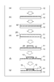
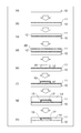
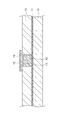
- FIG. 4 is a cross-sectional view illustrating a step after the step of FIG. 2 or 3 in the method for manufacturing a thin film transistor according to the first embodiment of the invention. It is sectional drawing which shows the structure of the thin-film transistor which concerns on Example 2 of this invention. It is a figure which shows the anodic oxide film SIMS analysis of Zr addition Al alloy. It is a figure which shows the characteristic of the gate insulating film of the thin-film transistor by the Example of this invention.
- FIG. 1 is a cross-sectional view showing an example of the structure of a thin film transistor (TFT) according to the present invention.
- An Na diffusion prevention film 11 formed on a glass substrate (insulating substrate) 10 and a predetermined pattern on the Na diffusion prevention film 11 are shown.
- Al or Al alloy gate electrode 12 shown in the figure shows a portion of the gate electrode
- a dense anodic oxide film formed on the surface of the gate electrode 12 by anodic oxidation using a non-aqueous solution 13 is disposed so as to surround the periphery of the gate electrode 12, has substantially the same height as the upper surface of the anodic oxide film 13 on the upper surface of the gate electrode 12, and is substantially flush with the upper surface of the anodic oxide film 13.
- FIG. 2A is a schematic view showing an example of a method for manufacturing the thin film transistor in the order of steps.
- an inexpensive soda glass or alkali glass substrate 10 is prepared as a substrate.
- the glass substrate 10 may be a large substrate capable of forming a large screen of 30 inches or more.
- the glass substrate 10 is treated with a 0.5 volume% hydrofluoric acid aqueous solution for 10 seconds and washed with pure water to remove surface contamination by lift-off.
- FIG. 2A an inexpensive soda glass or alkali glass substrate 10 is prepared as a substrate.
- the glass substrate 10 may be a large substrate capable of forming a large screen of 30 inches or more.
- the glass substrate 10 is treated with a 0.5 volume% hydrofluoric acid aqueous solution for 10 seconds and washed with pure water to remove surface contamination by lift-off.
- the coating type alkali diffusion preventing film 11 has a sodium diffusion preventing performance in a film thickness range of 150 to 300 nm. Sodium diffusion from the glass substrate 10 containing sodium into the film 11 is performed after firing and after annealing. There was almost no difference, and it was confirmed that the diffusion of sodium could be completely prevented.
- an Al alloy layer 12 ' is formed on the alkali diffusion preventing film 11 of the substrate to a thickness of 2 to 3 ⁇ m by sputtering.
- a photoresist 20 ' is applied thereon, and as shown in FIG. 2 (e), a resist is left in a predetermined pattern 20 by known exposure / development, and a dry mask is used as a mask.
- the Al alloy layer 12 ′ is formed into a predetermined gate electrode / wiring pattern 12 by etching.
- the resist 20 is removed, and the anodic oxidation film 13 is formed on the surface of the Al alloy 12 by the anodic oxidation using the non-aqueous solution described above as shown in FIG.
- the Al alloy used as a sputtering target is in mass%, the Mg concentration is 0.01% or less, the Zr concentration is more than 0.01%, and is less than 0.00%. 15% or less, the balance being Al and unavoidable impurities, and the elements of the unavoidable impurities being 0.01% or less, respectively.
- the elements of the inevitable impurities are mainly Si, Fe, and Cu, and in addition, Mn, Cr, Zn, etc. are inevitably mixed from raw metal, scrap, tools, etc. at the time of melting the alloy. .
- an alloy having such a purity for example, an alloy melted by using a high purity Al metal having an Al purity of 99.98% by mass or more obtained by a segregation method or a three-layer electrolysis method is used. Is preferred.
- the inevitable impurities are usually 0 for general-purpose Al alloys. About several percent is mixed, but this adversely affects the uniformity of the film produced by the anodizing treatment, so it is necessary to make it 0.01% or less.
- an amorphous Zr-added Al 2 O 3 film is formed on the surface of the Zr-added Al alloy layer 12 as an anodic oxide film 13 by anodization using a non-aqueous solution (0.1 ⁇ m). About 0.6 ⁇ m is provided.
- the non-aqueous solution used contains ethylene glycol or diethylene glycol as a solvent and contains pure water and adipic acid as solutes.
- the gate insulating film is preferably as thin as possible, the thickness of the anodic oxide film 13 is set to 0.1 ⁇ m.
- the resin is selected from the group consisting of acrylic resin, silicone resin, fluorine resin, polyimide resin, polyolefin resin, alicyclic olefin resin, and epoxy resin.
- a solution in which one or more resins are dissolved in a solvent is applied to the periphery of the gate electrode / wiring layer 12 with a slit coater and dried to approximately the same height as the gate electrode 12 and its upper surface anodic oxide film 13.
- a transparent resin layer 14 that is substantially flush with the anodic oxide film 13 is provided.
- FIGS. 3A to 3F are the same as the steps in FIGS. 2A to 2F, and the description thereof will be omitted.
- the transparent insulating film 14 ′ is formed beyond the height of the gate electrode / wiring 12 and the gate insulating film 13 on the upper surface thereof.
- the substrate 10 formed up to the transparent insulating film 14 ′ is placed in a microwave excitation type plasma processing apparatus, krypton gas and oxygen gas are introduced into the apparatus, and microwaves are further introduced into the apparatus to generate plasma. As shown in FIG.
- the surface of the transparent insulating film 14 ′ is removed by etch back, and the surface of the gate insulating film 13 is exposed. At this time, the exposed surface of the gate insulating film 13 is exposed to oxygen radicals generated by the plasma, so that oxidation proceeds and the film quality is improved.
- the gate electrode is interposed through the gate insulating film 13 in the metal surface microwave excitation plasma processing apparatus (MSEP).
- MSEP metal surface microwave excitation plasma processing apparatus
- the amorphous silicon film 15 and the n + -type amorphous silicon film 16 are continuously deposited by PECVD so as to cover 12, and the amorphous silicon film 15 other than on the gate electrode 12 and its peripheral part is formed by photolithography and known RIE. Part of 16 was removed.
- a film is formed in the order of Ti, Al, and Ti to form a source electrode and a drain electrode by a known sputtering method or the like, and patterning is performed by a photolithography method.
- the source electrode 17 and the drain electrode 18 were formed.
- the source region and the drain region were separated by etching the n + -type amorphous silicon film 16 by a known method using the formed source electrode 17 and drain electrode 18 as a mask.
- a silicon nitride film (not shown) was formed as a protective film by a known PECVD method to complete the thin film transistor of this example.
- the thin film transistor (TFT) 200 includes a Na diffusion prevention film 110 formed on a soda glass substrate 100 and a lower layer 121 formed in a predetermined pattern on the Na diffusion prevention film 110.
- the upper layer 122 is made of an Al—Zr alloy gate electrode / gate drive wiring layer 120 (the gate electrode portion is shown in the figure), and the gate electrode 120 has a dense surface formed by anodic oxidation using a non-aqueous solution. And an anodic oxide film 130.
- the illustrated TFT 200 is arranged so as to surround the periphery of the gate electrode / wiring layer 120, is formed up to the same height as the upper surface of the anodic oxide film 130 on the upper surface of the gate electrode 120, and A transparent resin layer 140 having substantially the same plane and an intrinsic amorphous silicon (i-aSi) layer 150 formed on the gate electrode 120 via the gate insulating film 130 are provided.
- the i-aSi layer 150 is provided with source and drain electrode connection regions.
- a high-concentration n-type amorphous silicon (n + -aSi) layer 160 is provided, and a lower layer 171 formed of Zr so as to contact the surface of the same layer 160 and Al.
- a source electrode 170 including the formed upper layer 172 is included.
- a high-concentration n-type amorphous silicon (n + -aSi) layer 160 is provided, and a lower layer 181 made of Zr and an upper layer made of Al so as to contact the surface of the layer 160.
- the exposed portions of the source electrode 170, the drain electrode 180, and the iaSi layer 150 are covered with a SiCN protective film 190, and the SiCN protective film 190 covers the upper surface of the device.
- an inexpensive soda glass substrate 100 is prepared as a substrate.
- the glass substrate 100 is treated with a 0.5 volume% hydrofluoric acid aqueous solution for 10 seconds and washed with pure water to remove surface contamination by lift-off.
- a solution obtained by dissolving a composition of ((CH 3 ) SiO 3/2 ) x (SiO 2 ) 1-x (where 0 ⁇ x ⁇ 1.0) in an organic solvent is applied to the surface of the soda glass substrate 100. Apply using a slit coater. And it is made to heat under reduced pressure and a solvent is removed completely. Specifically, heating is performed at 400 ° C.
- the transparent alkali diffusion preventing layer 110 having a thickness of 0.2 ⁇ m to 0.3 ⁇ m is formed.
- an Al layer 121 is formed to a thickness of 1.5 to 2.0 ⁇ m by sputtering on the alkali diffusion prevention film 110 of the substrate, and an Al alloy layer (including Zr: 0.1% by mass%) is formed thereon.
- the remaining Al (Mg is below the detection limit or 0.01% or less) 122 is formed into a thickness of 0.5 to 1.5 ⁇ m by sputtering, and a photoresist (not shown) is applied thereon.
- the resist is left in a predetermined pattern (gate electrode and gate drive wiring pattern) by known exposure / development, and the Al layer 121 and the Al alloy layer 122 are formed with the predetermined gate electrode / wiring pattern 120 by dry etching using the resist as a mask. To do. Next, the resist is removed, and the surface of the gate electrode / wiring layer 120 is anodized with a non-aqueous solution to form an anodized film 130.
- the Al layer 121 and the Al alloy layer 122 in this example are each 0.01% or less in terms of mass% of elements of inevitable impurities such as Si, Fe, Cu, Mn, Cr, and Zn, as described above. May be included. Further, as described above, the Al alloy layer 122 is in mass%, Mg concentration is 0.01 or less, Ce concentration is 0.01% or less, Zr concentration is more than 0.01% and 0.15% or less, The balance is preferably made of Al and inevitable impurities.
- an Al 2 O 3 film (on the surface of the Al alloy layer 122) is formed on the surfaces of the Al layer 121 and the Al alloy layer 122 by anodic oxidation using a non-aqueous solution.
- Zr is added in the formed part) to a thickness of 0.05 ⁇ m to 0.1 ⁇ m. This corresponds to 0.025 ⁇ m to 0.05 ⁇ m in EOT as a gate insulating film.
- the non-aqueous solution used was 79% ethylene glycol as a solvent, 20% pure water and 1.0% adipic acid (volume ratio) as a solute, or 79.5% diethylene glycol, 20% pure water and 0.5% adipic acid. It will be. At room temperature when the former is used and at 50 ° C.
- anodization is performed in a constant current mode with a current density of 0.1 mA / cm 2 to 0.2 mA / cm 2 , and then a constant voltage of 60 V to 30 V is applied. Anodize in voltage mode. Then, the anodized film is heat-treated at 300 ° C. for about 1 hour in an atmosphere of nitrogen gas and oxygen gas.
- a solution obtained by dissolving the alkali-soluble alicyclic olefin-based resin composition in a solvent is formed around the gate electrode / wiring layer 120 with a slit coater so as to exceed the height of the anodic oxide film 130 on the upper surface of the gate electrode 120.
- a transparent organic insulating film is formed.
- krypton gas and oxygen gas are introduced into the apparatus, and microwaves are further introduced into the apparatus to generate plasma, and the entire surface of the transparent organic insulating film is etched, The surface of the gate insulating film 130 is exposed.
- the exposed surface of the gate insulating film 130 is exposed to oxygen radicals generated by the plasma, and the oxidation proceeds to improve the film quality.
- the transparent organic insulating film 140 having the same height as the surface of the gate insulating film 130 is formed.
- an intrinsic amorphous silicon film is formed on the flat surface of the gate insulating film 130 and the transparent organic insulating film 140 by a PECVD method using a microwave-excited plasma processing apparatus. Further, an n + type amorphous silicon film is continuously deposited thereon in an amount of 0.05 to 0.1 ⁇ m. Further thereon, Zr is continuously deposited in an amount of 0.1 to 0.2 ⁇ m, and Al is continuously deposited thereon in an amount of 0.5 ⁇ m. Then, the Al / Zr / n + type amorphous silicon film / intrinsic amorphous silicon film is removed except for a predetermined pattern (on the gate electrode 120 and its peripheral portion) by a photolithography method and a known RIE method.
- an intrinsic amorphous silicon film 150 having a predetermined pattern (on the gate electrode 120 and its peripheral portion) is formed.
- the Al / Zr / n + type amorphous silicon film is etched away so that the source and drain are separated, and the n + type amorphous silicon film 160 in the source and drain regions, Al / Zr A source electrode 170 and an Al / Zr drain electrode 180 are formed.
- a SiCN film 190 is formed as a protective film by PECVD.
- wiring contact to the source / drain electrodes 170 and 180 is performed by providing a through hole in the SiCN protective film 190.
- a Zr-containing Al alloy layer 122 is provided on the upper layer of the gate electrode 120.
- the Zr-containing Al layer 122 can form a dense and high-quality anodic oxide film as compared with the case of the Al layer 121 alone.
- the Zr-added anodic oxide film 130 formed on the Zr-containing Al layer 122 can also be formed densely and with good quality (even if it is thin, it has good insulation performance and high breakdown voltage).
- a silicon nitride film or the like may be formed on the surface of the anodized insulating films 13 and 130 on the upper surface as necessary.
- a composite gate insulating film may be formed by CVD.
- the gate electrode / wiring is made of a Zr-added Al alloy in the embodiment, but an electrode of another material may be used inside or under the gate electrode / wiring.
- At least the upper surface of the gate electrode or wiring is composed of Zr-added Al, and the surface is oxidized by non-aqueous anodic oxidation to form a Zr-added Al 2 O 3 film, which is used as at least a part of the gate insulating film. Use it.
- FIG. 6 shows the results of the SISM analysis when the surface of Al containing 0.1% Zr is anodized with the above-described non-aqueous solution, thereby forming an anodic oxide film having a thickness of 300 nm.
- Zr was added to the anodized film formed by anodic oxidation with a non-aqueous solution on the surface of Al to which Zr was added.
- an Al film to which 0.1% of Zr is added is formed by sputtering, and an electric field strength E (MV / cm) is applied to the anodic oxide film having a thickness of 80 nm formed on the surface by anodization with a non-aqueous solution.
- E electric field strength
- J leakage current J
- FIG. 7 an 80 nm thick anode formed by sputtering an Al film added with 4.5% Mg, 1.0% Ce and 0.1% Zr, and formed on the surface by anodization with a non-aqueous solution Values for oxide films are also shown.
- anodic oxide film As the anodic oxide film, a 79% EG / 20% H 2 O / 1% ADA solution was used, and anodic oxidation at a constant current of 0.5 ⁇ A / cm 2 was performed at 23 ° C. for 2 hours after a constant voltage of 50 V. Thereafter, it was formed by heat treatment under reduced pressure in nitrogen and normal pressure in oxygen at 300 ° C. for 1 hour. As shown in FIG. 7, the anodic oxide film to which only Zr is added (“present invention” in FIG. 7) has a lower leakage current and a higher breakdown voltage than the comparative example, which is excellent. It became clear that it was a gate insulating film.
- the present invention can be applied to a display device such as a liquid crystal display device, an organic EL device, an inorganic EL device, etc. to increase the size of the display device, and can also be applied to wiring other than the display device.
- a display device such as a liquid crystal display device, an organic EL device, an inorganic EL device, etc. to increase the size of the display device, and can also be applied to wiring other than the display device.
Landscapes
- Thin Film Transistor (AREA)
- Engineering & Computer Science (AREA)
- Manufacturing & Machinery (AREA)
- Electrodes Of Semiconductors (AREA)
- Physical Vapour Deposition (AREA)
Abstract
La présente invention porte sur un dispositif à semi-conducteurs comprenant : une électrode de grille disposée sur un substrat et contenant de l'aluminium (Al) et du zirconium (Zr) ; un film d'isolation de grille disposé de façon à recouvrir au moins la surface supérieure de l'électrode de grille et contenant de l'aluminium (Al) et du zirconium (Zr), et une couche d'isolation disposée sur le substrat de façon à entourer l'électrode de grille.
Priority Applications (3)
| Application Number | Priority Date | Filing Date | Title |
|---|---|---|---|
| PCT/JP2011/000530 WO2012104902A1 (fr) | 2011-01-31 | 2011-01-31 | Dispositif à semi-conducteurs et son procédé de fabrication |
| JP2012555554A JPWO2012104902A1 (ja) | 2011-01-31 | 2011-01-31 | 半導体装置及びその製造方法 |
| US13/949,284 US8941091B2 (en) | 2011-01-31 | 2013-07-24 | Gate electrode comprising aluminum and zirconium |
Applications Claiming Priority (1)
| Application Number | Priority Date | Filing Date | Title |
|---|---|---|---|
| PCT/JP2011/000530 WO2012104902A1 (fr) | 2011-01-31 | 2011-01-31 | Dispositif à semi-conducteurs et son procédé de fabrication |
Related Child Applications (1)
| Application Number | Title | Priority Date | Filing Date |
|---|---|---|---|
| US13/949,284 Continuation US8941091B2 (en) | 2011-01-31 | 2013-07-24 | Gate electrode comprising aluminum and zirconium |
Publications (1)
| Publication Number | Publication Date |
|---|---|
| WO2012104902A1 true WO2012104902A1 (fr) | 2012-08-09 |
Family
ID=46602156
Family Applications (1)
| Application Number | Title | Priority Date | Filing Date |
|---|---|---|---|
| PCT/JP2011/000530 Ceased WO2012104902A1 (fr) | 2011-01-31 | 2011-01-31 | Dispositif à semi-conducteurs et son procédé de fabrication |
Country Status (3)
| Country | Link |
|---|---|
| US (1) | US8941091B2 (fr) |
| JP (1) | JPWO2012104902A1 (fr) |
| WO (1) | WO2012104902A1 (fr) |
Cited By (1)
| Publication number | Priority date | Publication date | Assignee | Title |
|---|---|---|---|---|
| JP2018142598A (ja) * | 2017-02-27 | 2018-09-13 | 地方独立行政法人大阪産業技術研究所 | 有機絶縁性薄膜、有機トランジスタ、キャパシタおよび有機絶縁性薄膜の製造方法 |
Families Citing this family (2)
| Publication number | Priority date | Publication date | Assignee | Title |
|---|---|---|---|---|
| US9719175B2 (en) | 2014-09-30 | 2017-08-01 | Kennametal Inc. | Multilayer structured coatings for cutting tools |
| KR102652258B1 (ko) * | 2016-07-12 | 2024-03-28 | 에이비엠 주식회사 | 금속부품 및 그 제조 방법 및 금속부품을 구비한 공정챔버 |
Citations (8)
| Publication number | Priority date | Publication date | Assignee | Title |
|---|---|---|---|---|
| JPH0285826A (ja) * | 1988-09-22 | 1990-03-27 | Hitachi Ltd | 表示パネル |
| JPH06326130A (ja) * | 1993-05-17 | 1994-11-25 | Matsushita Electric Ind Co Ltd | 平坦化方法と平坦化素子 |
| JPH07245434A (ja) * | 1994-03-02 | 1995-09-19 | Seiko Epson Corp | 配線膜の製造方法及び非線形抵抗素子の製造方法及び薄膜トランジスタの製造方法及び半導体装置の製造方法及び配線膜及び非線形抵抗素子及び薄膜トランジスタ及び液晶表示装置及び半導体装置 |
| JPH10319441A (ja) * | 1997-03-14 | 1998-12-04 | Fujitsu Ltd | 薄膜装置の製造方法及び薄膜装置 |
| JPH1152415A (ja) * | 1997-07-29 | 1999-02-26 | Toshiba Corp | 液晶表示素子 |
| JP2006210477A (ja) * | 2005-01-26 | 2006-08-10 | Idemitsu Kosan Co Ltd | 薄膜トランジスタ及びその製造方法並びに薄膜トランジスタ基板及びその製造方法並びに該薄膜トランジスタを用いた液晶表示装置及び有機el表示装置並びに透明導電積層基板 |
| JP2007043131A (ja) * | 2005-07-05 | 2007-02-15 | Tohoku Univ | 薄膜トランジスタ、配線板、及びそれらの製造方法 |
| JP2009021621A (ja) * | 2001-10-30 | 2009-01-29 | Semiconductor Energy Lab Co Ltd | 半導体装置の作製方法 |
Family Cites Families (4)
| Publication number | Priority date | Publication date | Assignee | Title |
|---|---|---|---|---|
| DE1955396B2 (de) * | 1968-11-05 | 1971-09-30 | Elektrolytkondensator und verfahren zu seiner herstellung | |
| TW200721501A (en) | 2005-07-05 | 2007-06-01 | Univ Tohoku | Thin-film transistor, wiring board and methods of producing the thin-film transistor and the wiring board |
| US20080207077A1 (en) * | 2007-02-26 | 2008-08-28 | 3M Innovative Properties Company | Fabrication of backplanes allowing relaxed alignment tolerance |
| KR20120048590A (ko) | 2009-07-31 | 2012-05-15 | 고쿠리츠 다이가쿠 호진 도호쿠 다이가쿠 | 반도체 장치, 반도체 장치의 제조 방법, 및 표시 장치 |
-
2011
- 2011-01-31 JP JP2012555554A patent/JPWO2012104902A1/ja active Pending
- 2011-01-31 WO PCT/JP2011/000530 patent/WO2012104902A1/fr not_active Ceased
-
2013
- 2013-07-24 US US13/949,284 patent/US8941091B2/en not_active Expired - Fee Related
Patent Citations (8)
| Publication number | Priority date | Publication date | Assignee | Title |
|---|---|---|---|---|
| JPH0285826A (ja) * | 1988-09-22 | 1990-03-27 | Hitachi Ltd | 表示パネル |
| JPH06326130A (ja) * | 1993-05-17 | 1994-11-25 | Matsushita Electric Ind Co Ltd | 平坦化方法と平坦化素子 |
| JPH07245434A (ja) * | 1994-03-02 | 1995-09-19 | Seiko Epson Corp | 配線膜の製造方法及び非線形抵抗素子の製造方法及び薄膜トランジスタの製造方法及び半導体装置の製造方法及び配線膜及び非線形抵抗素子及び薄膜トランジスタ及び液晶表示装置及び半導体装置 |
| JPH10319441A (ja) * | 1997-03-14 | 1998-12-04 | Fujitsu Ltd | 薄膜装置の製造方法及び薄膜装置 |
| JPH1152415A (ja) * | 1997-07-29 | 1999-02-26 | Toshiba Corp | 液晶表示素子 |
| JP2009021621A (ja) * | 2001-10-30 | 2009-01-29 | Semiconductor Energy Lab Co Ltd | 半導体装置の作製方法 |
| JP2006210477A (ja) * | 2005-01-26 | 2006-08-10 | Idemitsu Kosan Co Ltd | 薄膜トランジスタ及びその製造方法並びに薄膜トランジスタ基板及びその製造方法並びに該薄膜トランジスタを用いた液晶表示装置及び有機el表示装置並びに透明導電積層基板 |
| JP2007043131A (ja) * | 2005-07-05 | 2007-02-15 | Tohoku Univ | 薄膜トランジスタ、配線板、及びそれらの製造方法 |
Cited By (1)
| Publication number | Priority date | Publication date | Assignee | Title |
|---|---|---|---|---|
| JP2018142598A (ja) * | 2017-02-27 | 2018-09-13 | 地方独立行政法人大阪産業技術研究所 | 有機絶縁性薄膜、有機トランジスタ、キャパシタおよび有機絶縁性薄膜の製造方法 |
Also Published As
| Publication number | Publication date |
|---|---|
| US8941091B2 (en) | 2015-01-27 |
| US20130307092A1 (en) | 2013-11-21 |
| JPWO2012104902A1 (ja) | 2014-07-03 |
Similar Documents
| Publication | Publication Date | Title |
|---|---|---|
| WO2011013600A1 (fr) | Dispositif semi-conducteur, procédé de fabrication d'un dispositif semi-conducteur et dispositif d'affichage | |
| JP5358799B2 (ja) | 金属酸化物膜、積層体、金属部材並びにその製造方法 | |
| TWI583776B (zh) | 蝕刻劑組合物、金屬圖案的形成方法和陣列基板的製法 | |
| CN104471091A (zh) | 阳极氧化处理性优异的铝合金和阳极氧化处理铝合金构件 | |
| KR20070077113A (ko) | 알루미늄계 금속막 및 몰리브덴계 금속막의 적층막용에칭액 | |
| JP2009177102A (ja) | 半導体装置の電極の製造方法 | |
| CN1092840C (zh) | 制造半导体器件的方法 | |
| WO2012104902A1 (fr) | Dispositif à semi-conducteurs et son procédé de fabrication | |
| JP2007009331A (ja) | エッチング組成物、及び液晶表示装置用アレイ基板の製造方法 | |
| TWI611483B (zh) | 薄膜電晶體製造方法及薄膜電晶體 | |
| US11248306B2 (en) | Anodic-oxidation equipment, anodic-oxidation method, and method for producing cathode of anodic-oxidation equipment | |
| TW201843357A (zh) | 化學品液、含有鋁之基材之化學處理方法、化學處理完畢之基材、鋁電解電容器用電極材及電容器 | |
| US20250188638A1 (en) | Method of manufacturing structure having anodized parts | |
| US12598934B2 (en) | Method of manufacturing structure having multi metal layers | |
| KR20130051239A (ko) | 식각액 조성물, 금속 패턴의 형성 방법 및 표시 기판의 제조 방법 | |
| JP2006261553A (ja) | 半導体装置及びその製造方法 | |
| KR101737034B1 (ko) | 박막트랜지스터 제조 방법 및 박막트랜지스터 | |
| KR102247235B1 (ko) | 티타늄막 식각액 조성물 | |
| US20030098767A1 (en) | Process for fabricating an electronic component incorporating an inductive microcomponent | |
| KR102092338B1 (ko) | 액정 표시 장치용 어레이 기판의 제조 방법 | |
| JP3997035B2 (ja) | 金属酸化物皮膜形成用化成液 | |
| JP4397899B2 (ja) | 半導体装置の作製方法 | |
| JP2008071671A (ja) | 有機el素子アレイ及びその作製方法 | |
| JPS5934798B2 (ja) | 陽極酸化方法 | |
| JP2000323662A5 (ja) | 液晶表示装置、半導体装置及びコンデンサー並びにそれらの作製方法 |
Legal Events
| Date | Code | Title | Description |
|---|---|---|---|
| 121 | Ep: the epo has been informed by wipo that ep was designated in this application |
Ref document number: 11857576 Country of ref document: EP Kind code of ref document: A1 |
|
| ENP | Entry into the national phase |
Ref document number: 2012555554 Country of ref document: JP Kind code of ref document: A |
|
| NENP | Non-entry into the national phase |
Ref country code: DE |
|
| 122 | Ep: pct application non-entry in european phase |
Ref document number: 11857576 Country of ref document: EP Kind code of ref document: A1 |