WO2012114849A1 - Élément photorécepteur et son procédé de fabrication - Google Patents
Élément photorécepteur et son procédé de fabrication Download PDFInfo
- Publication number
- WO2012114849A1 WO2012114849A1 PCT/JP2012/052478 JP2012052478W WO2012114849A1 WO 2012114849 A1 WO2012114849 A1 WO 2012114849A1 JP 2012052478 W JP2012052478 W JP 2012052478W WO 2012114849 A1 WO2012114849 A1 WO 2012114849A1
- Authority
- WO
- WIPO (PCT)
- Prior art keywords
- layer
- light receiving
- receiving element
- semiconductor layer
- semiconductor
- Prior art date
- Legal status (The legal status is an assumption and is not a legal conclusion. Google has not performed a legal analysis and makes no representation as to the accuracy of the status listed.)
- Ceased
Links
Images


Classifications
-
- B—PERFORMING OPERATIONS; TRANSPORTING
- B82—NANOTECHNOLOGY
- B82Y—SPECIFIC USES OR APPLICATIONS OF NANOSTRUCTURES; MEASUREMENT OR ANALYSIS OF NANOSTRUCTURES; MANUFACTURE OR TREATMENT OF NANOSTRUCTURES
- B82Y20/00—Nanooptics, e.g. quantum optics or photonic crystals
-
- H—ELECTRICITY
- H10—SEMICONDUCTOR DEVICES; ELECTRIC SOLID-STATE DEVICES NOT OTHERWISE PROVIDED FOR
- H10F—INORGANIC SEMICONDUCTOR DEVICES SENSITIVE TO INFRARED RADIATION, LIGHT, ELECTROMAGNETIC RADIATION OF SHORTER WAVELENGTH OR CORPUSCULAR RADIATION
- H10F77/00—Constructional details of devices covered by this subclass
- H10F77/10—Semiconductor bodies
- H10F77/14—Shape of semiconductor bodies; Shapes, relative sizes or dispositions of semiconductor regions within semiconductor bodies
- H10F77/143—Shape of semiconductor bodies; Shapes, relative sizes or dispositions of semiconductor regions within semiconductor bodies comprising quantum structures
-
- C—CHEMISTRY; METALLURGY
- C30—CRYSTAL GROWTH
- C30B—SINGLE-CRYSTAL GROWTH; UNIDIRECTIONAL SOLIDIFICATION OF EUTECTIC MATERIAL OR UNIDIRECTIONAL DEMIXING OF EUTECTOID MATERIAL; REFINING BY ZONE-MELTING OF MATERIAL; PRODUCTION OF A HOMOGENEOUS POLYCRYSTALLINE MATERIAL WITH DEFINED STRUCTURE; SINGLE CRYSTALS OR HOMOGENEOUS POLYCRYSTALLINE MATERIAL WITH DEFINED STRUCTURE; AFTER-TREATMENT OF SINGLE CRYSTALS OR A HOMOGENEOUS POLYCRYSTALLINE MATERIAL WITH DEFINED STRUCTURE; APPARATUS THEREFOR
- C30B25/00—Single-crystal growth by chemical reaction of reactive gases, e.g. chemical vapour-deposition growth
- C30B25/02—Epitaxial-layer growth
- C30B25/18—Epitaxial-layer growth characterised by the substrate
- C30B25/183—Epitaxial-layer growth characterised by the substrate being provided with a buffer layer, e.g. a lattice matching layer
-
- C—CHEMISTRY; METALLURGY
- C30—CRYSTAL GROWTH
- C30B—SINGLE-CRYSTAL GROWTH; UNIDIRECTIONAL SOLIDIFICATION OF EUTECTIC MATERIAL OR UNIDIRECTIONAL DEMIXING OF EUTECTOID MATERIAL; REFINING BY ZONE-MELTING OF MATERIAL; PRODUCTION OF A HOMOGENEOUS POLYCRYSTALLINE MATERIAL WITH DEFINED STRUCTURE; SINGLE CRYSTALS OR HOMOGENEOUS POLYCRYSTALLINE MATERIAL WITH DEFINED STRUCTURE; AFTER-TREATMENT OF SINGLE CRYSTALS OR A HOMOGENEOUS POLYCRYSTALLINE MATERIAL WITH DEFINED STRUCTURE; APPARATUS THEREFOR
- C30B29/00—Single crystals or homogeneous polycrystalline material with defined structure characterised by the material or by their shape
- C30B29/10—Inorganic compounds or compositions
- C30B29/40—AIIIBV compounds wherein A is B, Al, Ga, In or Tl and B is N, P, As, Sb or Bi
-
- C—CHEMISTRY; METALLURGY
- C30—CRYSTAL GROWTH
- C30B—SINGLE-CRYSTAL GROWTH; UNIDIRECTIONAL SOLIDIFICATION OF EUTECTIC MATERIAL OR UNIDIRECTIONAL DEMIXING OF EUTECTOID MATERIAL; REFINING BY ZONE-MELTING OF MATERIAL; PRODUCTION OF A HOMOGENEOUS POLYCRYSTALLINE MATERIAL WITH DEFINED STRUCTURE; SINGLE CRYSTALS OR HOMOGENEOUS POLYCRYSTALLINE MATERIAL WITH DEFINED STRUCTURE; AFTER-TREATMENT OF SINGLE CRYSTALS OR A HOMOGENEOUS POLYCRYSTALLINE MATERIAL WITH DEFINED STRUCTURE; APPARATUS THEREFOR
- C30B29/00—Single crystals or homogeneous polycrystalline material with defined structure characterised by the material or by their shape
- C30B29/10—Inorganic compounds or compositions
- C30B29/40—AIIIBV compounds wherein A is B, Al, Ga, In or Tl and B is N, P, As, Sb or Bi
- C30B29/42—Gallium arsenide
-
- C—CHEMISTRY; METALLURGY
- C30—CRYSTAL GROWTH
- C30B—SINGLE-CRYSTAL GROWTH; UNIDIRECTIONAL SOLIDIFICATION OF EUTECTIC MATERIAL OR UNIDIRECTIONAL DEMIXING OF EUTECTOID MATERIAL; REFINING BY ZONE-MELTING OF MATERIAL; PRODUCTION OF A HOMOGENEOUS POLYCRYSTALLINE MATERIAL WITH DEFINED STRUCTURE; SINGLE CRYSTALS OR HOMOGENEOUS POLYCRYSTALLINE MATERIAL WITH DEFINED STRUCTURE; AFTER-TREATMENT OF SINGLE CRYSTALS OR A HOMOGENEOUS POLYCRYSTALLINE MATERIAL WITH DEFINED STRUCTURE; APPARATUS THEREFOR
- C30B29/00—Single crystals or homogeneous polycrystalline material with defined structure characterised by the material or by their shape
- C30B29/60—Single crystals or homogeneous polycrystalline material with defined structure characterised by the material or by their shape characterised by shape
- C30B29/68—Crystals with laminate structure, e.g. "superlattices"
-
- H—ELECTRICITY
- H10—SEMICONDUCTOR DEVICES; ELECTRIC SOLID-STATE DEVICES NOT OTHERWISE PROVIDED FOR
- H10F—INORGANIC SEMICONDUCTOR DEVICES SENSITIVE TO INFRARED RADIATION, LIGHT, ELECTROMAGNETIC RADIATION OF SHORTER WAVELENGTH OR CORPUSCULAR RADIATION
- H10F30/00—Individual radiation-sensitive semiconductor devices in which radiation controls the flow of current through the devices, e.g. photodetectors
- H10F30/20—Individual radiation-sensitive semiconductor devices in which radiation controls the flow of current through the devices, e.g. photodetectors the devices having potential barriers, e.g. phototransistors
- H10F30/21—Individual radiation-sensitive semiconductor devices in which radiation controls the flow of current through the devices, e.g. photodetectors the devices having potential barriers, e.g. phototransistors the devices being sensitive to infrared, visible or ultraviolet radiation
- H10F30/22—Individual radiation-sensitive semiconductor devices in which radiation controls the flow of current through the devices, e.g. photodetectors the devices having potential barriers, e.g. phototransistors the devices being sensitive to infrared, visible or ultraviolet radiation the devices having only one potential barrier, e.g. photodiodes
- H10F30/222—Individual radiation-sensitive semiconductor devices in which radiation controls the flow of current through the devices, e.g. photodetectors the devices having potential barriers, e.g. phototransistors the devices being sensitive to infrared, visible or ultraviolet radiation the devices having only one potential barrier, e.g. photodiodes the potential barrier being a PN heterojunction
-
- H—ELECTRICITY
- H10—SEMICONDUCTOR DEVICES; ELECTRIC SOLID-STATE DEVICES NOT OTHERWISE PROVIDED FOR
- H10F—INORGANIC SEMICONDUCTOR DEVICES SENSITIVE TO INFRARED RADIATION, LIGHT, ELECTROMAGNETIC RADIATION OF SHORTER WAVELENGTH OR CORPUSCULAR RADIATION
- H10F71/00—Manufacture or treatment of devices covered by this subclass
- H10F71/127—The active layers comprising only Group III-V materials, e.g. GaAs or InP
- H10F71/1272—The active layers comprising only Group III-V materials, e.g. GaAs or InP comprising at least three elements, e.g. GaAlAs or InGaAsP
-
- H—ELECTRICITY
- H10—SEMICONDUCTOR DEVICES; ELECTRIC SOLID-STATE DEVICES NOT OTHERWISE PROVIDED FOR
- H10F—INORGANIC SEMICONDUCTOR DEVICES SENSITIVE TO INFRARED RADIATION, LIGHT, ELECTROMAGNETIC RADIATION OF SHORTER WAVELENGTH OR CORPUSCULAR RADIATION
- H10F77/00—Constructional details of devices covered by this subclass
- H10F77/10—Semiconductor bodies
- H10F77/14—Shape of semiconductor bodies; Shapes, relative sizes or dispositions of semiconductor regions within semiconductor bodies
- H10F77/146—Superlattices; Multiple quantum well structures
-
- Y—GENERAL TAGGING OF NEW TECHNOLOGICAL DEVELOPMENTS; GENERAL TAGGING OF CROSS-SECTIONAL TECHNOLOGIES SPANNING OVER SEVERAL SECTIONS OF THE IPC; TECHNICAL SUBJECTS COVERED BY FORMER USPC CROSS-REFERENCE ART COLLECTIONS [XRACs] AND DIGESTS
- Y02—TECHNOLOGIES OR APPLICATIONS FOR MITIGATION OR ADAPTATION AGAINST CLIMATE CHANGE
- Y02E—REDUCTION OF GREENHOUSE GAS [GHG] EMISSIONS, RELATED TO ENERGY GENERATION, TRANSMISSION OR DISTRIBUTION
- Y02E10/00—Energy generation through renewable energy sources
- Y02E10/50—Photovoltaic [PV] energy
- Y02E10/544—Solar cells from Group III-V materials
-
- Y—GENERAL TAGGING OF NEW TECHNOLOGICAL DEVELOPMENTS; GENERAL TAGGING OF CROSS-SECTIONAL TECHNOLOGIES SPANNING OVER SEVERAL SECTIONS OF THE IPC; TECHNICAL SUBJECTS COVERED BY FORMER USPC CROSS-REFERENCE ART COLLECTIONS [XRACs] AND DIGESTS
- Y02—TECHNOLOGIES OR APPLICATIONS FOR MITIGATION OR ADAPTATION AGAINST CLIMATE CHANGE
- Y02P—CLIMATE CHANGE MITIGATION TECHNOLOGIES IN THE PRODUCTION OR PROCESSING OF GOODS
- Y02P70/00—Climate change mitigation technologies in the production process for final industrial or consumer products
- Y02P70/50—Manufacturing or production processes characterised by the final manufactured product
Definitions
- the present invention relates to a light receiving element and a method for manufacturing the same. More specifically, a light-receiving element including a light-receiving layer having a multiple quantum well structure (Multiple-Quantum ⁇ Well, hereinafter referred to as MQW) that secures sensitivity in the near-infrared wavelength region of 1.5 ⁇ m to 1.8 ⁇ m and its It relates to a manufacturing method.
- MQW multiple quantum well structure
- Non-Patent Document 1 proposes a photodiode having a cut-off wavelength of 2.39 ⁇ m by forming an InGaAs / GaAsSb type 2 MQW on an InP substrate and a pn junction formed by a p-type or n-type epitaxial layer. Sensitivity characteristics with wavelengths of 1.7 ⁇ m to 2.7 ⁇ m are shown.
- Non-Patent Document 2 shows the sensitivity characteristic (200K, 250K, 295K) of a wavelength of 1 ⁇ m to 3 ⁇ m of a light receiving element having a type 2 MQW light receiving layer in which 150 pairs of InGaAs 5 nm and GaAsSb 5 nm are stacked as a pair.
- Patent Document 1 gives an InP substrate and a lattice constant smaller than the lattice constant of the InP substrate formed on the InP substrate in order to slightly expand the upper limit wavelength of the light receiving region for optical communication.
- a photodiode including, in a light-receiving layer, In 0.53 Ga 0.47 As (first absorption layer) having a composition and In 0.55 Ga 0.45 As (second absorption layer) having a composition that provides a large lattice constant. Proposed. According to this, the light receiving area can be lengthened to a wavelength of about 1700 nm.
- the important absorption band of the substance is concentrated in the wavelength range of 1.5 ⁇ m to 1.8 ⁇ m, if a clear image with sufficiently high sensitivity can be obtained in this wavelength range of 1.5 ⁇ m to 1.8 ⁇ m, Use can be promoted.
- the sensitivity suddenly decreases from around a slightly long wavelength of 1.6 ⁇ m (see FIG. 6). This is because photoelectric current is generated by photoelectric conversion of both type 2 transition and type 1 transition. Due to this influence, the contribution of the type 1 transition is reduced from around the wavelength of 1.65 ⁇ m.
- the light receiving element of the present invention is a light receiving element made of a III-V group compound semiconductor formed on an InP substrate.
- the light receiving element includes a buffer layer positioned in contact with the InP substrate and a light receiving layer positioned in contact with the buffer layer.
- the light receiving layer is formed by alternately laminating a first semiconductor layer having a band gap energy of 0.73 eV or less and a second semiconductor layer having a band gap energy larger than the band gap energy of the first semiconductor layer. 50 pairs or more are included, the first semiconductor layer and the second semiconductor layer form a strain compensation quantum well structure, and the thicknesses of the first semiconductor layer and the second semiconductor layer are both 1 nm or more and 10 nm or less. It is characterized by.
- the band gap energy of the first semiconductor layer is 0.73 eV or less, high light receiving sensitivity can be obtained at a wavelength of 1.7 ⁇ m to 1.8 ⁇ m based on the type 1 transition in the first semiconductor layer.
- the first semiconductor layer has a larger lattice constant than the InP substrate, while the second semiconductor layer has a smaller lattice constant. Compressive stress and tensile stress are distributed in the latter, and both form a strain compensated quantum well structure.
- the first semiconductor layer / second semiconductor layer is 50 pairs or more, and the thickness of each semiconductor layer is 1 nm or more and 10 nm or less, so that the compressive strain and tensile strain due to lattice mismatch are balanced and the strain is macroscopically. The influence can be reduced. By avoiding the accumulation of this strain, the crystallinity can be improved and an increase in dark current can be prevented. That is, dark current can be kept low while having high light receiving sensitivity in the vicinity of a wavelength of 1.5 ⁇ m to 1.8 ⁇ m.
- MCT HgCdTe
- the first semiconductor layer and the second semiconductor layer can be (1) a type 2 multiple quantum well structure or (2) the same compound semiconductor having a different composition.
- the strain compensation quantum well structure may be (1) a type 2 multiple quantum well structure, or (2) a composition having a different composition, for example, InGaAs may be used.
- the dark current is kept low while having high light receiving sensitivity in the vicinity of the wavelength of 1.5 ⁇ m to 1.8 ⁇ m where the absorption bands important for the substance are concentrated. be able to.
- the total film thickness in the light receiving layer of the first semiconductor layer is preferably 0.5 ⁇ m or more. As a result, it is possible to ensure sensitivity especially at the upper limit near the wavelength of 1.75 ⁇ m. The light reception in the vicinity of the wavelength of 1.75 ⁇ m is due to the type 1 transition in the bulk of the first semiconductor layer. Therefore, the sensitivity can be ensured by setting the total film thickness to 0.5 ⁇ m or more.
- the band gap energy of the buffer layer is preferably larger than the band gap energy of either the first semiconductor layer or the second semiconductor layer. This prevents light from being absorbed by the buffer layer in the case of substrate backside incidence (necessary for two-dimensional array of pixels). Further, the band gap energy of InP (substrate) is 1.27 eV, and naturally, there is no possibility of absorbing light in the wavelength region currently in question.
- the first semiconductor layer can be In x Ga 1-x As (0.56 ⁇ x ⁇ 0.68). This makes it possible to obtain a first semiconductor layer that can reliably receive light with a wavelength of 1.7 ⁇ m to 1.8 ⁇ m in the type 1 transition.
- the second semiconductor layer can be In y Ga 1-y As (0.38 ⁇ y ⁇ 0.50).
- the strain compensation quantum well structure can be easily formed by combining the second semiconductor layer with a lattice constant smaller than InP and the first semiconductor layer having a lattice constant larger than InP.
- the crystallinity of the entire epitaxial layer including the window layer can be improved, and the dark current can be reduced.
- this second semiconductor layer can also receive light by the type 1 transition, but the upper limit of the wavelength that can be received is in a range shorter than 1.7 ⁇ m.
- the second semiconductor layer can be GaAs z Sb 1-z (0.54 ⁇ z ⁇ 0.66). Also in this case, the strain compensation quantum well structure can be easily formed by combining the second semiconductor layer with a lattice constant smaller than that of InP and the first semiconductor layer having a lattice constant larger than that of InP. In this case, since Sb that is difficult to handle is reduced, it is preferable for enhancing the crystallinity of the entire epitaxial layer and suppressing dark current. In this case, type 2 transition is possible, and not only the long wavelength side with a wavelength of 1.8 ⁇ m or longer, but also light in the wavelength range of 1.7 ⁇ m to 1.8 ⁇ m, which is the focal point, is received by the type 2 transition. can do. That is, not only light having a wavelength of 1.7 ⁇ m to 1.8 ⁇ m due to the type 1 transition by the first semiconductor layer but also light having a wavelength of 1.7 ⁇ m to 1.8 ⁇ m can be received by the type 2 transition.
- the all-organic metal vapor phase growth method refers to a growth method in which an organic metal raw material composed of a compound of an organic substance and a metal is used for all the raw materials for vapor phase growth, and is referred to as a total organic MOVPE method.
- the buffer layer can include P.
- Examples of cases where P is contained in the buffer layer include an InP buffer layer and an InGaAsP buffer layer. These buffer layers are easy to grow a good crystalline thin film. For this reason, the crystallinity of the light receiving layer (first and second semiconductor layers) grown in contact with the buffer layer can be improved, and as a result, the dark current can be lowered.
- a substrate back surface incident structure for making the back surface of the InP substrate the incident surface can be provided.
- the structure in which light is incident from the back side of the substrate means (1) bonding bumps provided on the pixel electrode on the surface side of the epitaxial layer (the readout circuit covers the surface side of the epitaxial layer), (2) An anti-reflection film (AR film) provided on the back side of the substrate, (3) a two-dimensional arrangement of light receiving elements (pixels) as a basic unit, which must be incident on the back side of the substrate (others) An example structure will be described later).
- the substrate backside incident structure described above it is possible to manufacture a light receiving element having two-dimensionally arrayed pixels while maintaining a low dark current and ensuring high sensitivity.
- III-V group compound semiconductor diffusion concentration distribution adjustment layer having a pn junction at the front end of the impurity introduced by selective diffusion and in contact with the upper surface of the light receiving layer opposite to the InP substrate, and adjustment of the diffusion concentration distribution thereof And a window layer containing P in contact with the layer, and the band gap energy of the diffusion concentration distribution adjusting layer is preferably made smaller than the band gap energy of the window layer.
- a light receiving element made of a III-V group compound semiconductor formed on an InP substrate is manufactured.
- This manufacturing method includes a step of forming a buffer layer on an InP substrate, a first semiconductor layer having a band gap of 0.73 eV or less on the buffer layer, and a first semiconductor layer having a band gap larger than that of the first semiconductor layer. And forming a light-receiving layer having a multiple quantum well structure by alternately stacking 50 pairs or more of both the first and second semiconductor layers with a thickness of 1 nm to 10 nm.
- the growth is performed at a growth temperature or a substrate temperature of 600 ° C. or less by a total organometallic vapor phase growth method.
- the light receiving layer has a strain compensated quantum well structure, and it is important whether or not good crystallinity can be obtained.
- the growth temperature or the substrate temperature can be lowered, so that the degree of crystallinity degradation due to thermal expansion caused by the temperature difference can be kept low when cooling after growth.
- the growth temperature or the substrate temperature is a substrate surface temperature monitored by a pyrometer including an infrared camera and an infrared spectrometer. Accordingly, although it is the substrate surface temperature, strictly speaking, it is the temperature of the epitaxial layer surface in a state where a film is formed on the substrate.
- a substrate temperature, a growth temperature, and a film formation temperature There are various names such as a substrate temperature, a growth temperature, and a film formation temperature, and all refer to the monitored temperatures.
- a step of forming a group III-V compound semiconductor layer on the light-receiving layer, and from the start of forming the light-receiving layer until the end of the formation of the group III-V compound semiconductor layer, the same by the all-organic metal vapor phase epitaxy method It is preferable to grow in the deposition chamber.
- all metal organic vapor phase epitaxy all metal organic vapor phase epitaxy
- the dark current can be lowered with a sufficiently high sensitivity stably in the near infrared wavelength range of 1.5 ⁇ m to 1.8 ⁇ m.
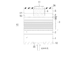
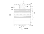
- the light-receiving layer 3 has a multiple quantum well structure formed by stacking 200 pairs of In 0.59 Ga 0.41 As3a and GaAs 0.57 Sb 0.43 3b.
- the film thicknesses of In 0.59 Ga 0.41 As3a and GaAs 0.57 Sb 0.43 3b in the quantum well are both 5 nm.
- the oxygen and carbon concentrations are both less than 1 ⁇ 10 17 cm ⁇ 3 .
- the light receiving layer 103 has a multiple quantum well structure formed by stacking 200 pairs of In 0.53 Ga 0.47 As 103 a and GaAs 0.51 Sb 0.49 103 b.
- the film thicknesses of In 0.53 Ga 0.47 As and GaAs 0.51 Sb 0.49 in the quantum well are both 5 nm. It is a figure which shows the wavelength dependence of the light reception sensitivity of the light receiving element of FIG. It is a figure which shows the light receiving element in Embodiment 2 of this invention.
- the light-receiving layer 3 has a multiple quantum well structure formed by stacking 200 pairs of In 0.59 Ga 0.41 As3a and In 0.47 Ga 0.53 As3c.
- the thicknesses of In 0.59 Ga 0.41 As3a and In 0.47 Ga 0.53 As3c in the quantum well are both 5 nm.
- the oxygen and carbon concentrations are both less than 1 ⁇ 10 17 cm ⁇ 3 . It is a figure which shows the wavelength dependence of the light reception sensitivity of the light receiving element of FIG. It is a flowchart of the manufacturing method of the light receiving element shown in FIG.
- the p-type region 6 is formed by selectively diffusing Zn of the p-type impurity from the opening of the selective diffusion mask pattern 36 of the SiN film. It is diffused by using the selective diffusion mask pattern 36 of the SiN film that the periphery is limited in a plane and is introduced into the inside of the periphery of the light receiving element 10 and the light receiving part is formed inside the periphery. It is realized by.
- a p-side electrode 11 made of AuZn is provided in the p-type region 6, and an n-side electrode 12 made of AuGeNi is provided in ohmic contact with the back surface of the InP substrate 1.
- the InP substrate 1 is doped with n-type impurities to ensure a predetermined level of conductivity.
- an AR (Anti-reflection) film 35 made of SiON or the like covers the back surface of the InP substrate 1.
- the AR film 35 disposed on the back surface of the InP substrate 1 may be regarded as a structure for entering from the substrate side.
- disposing the pixel electrode (p-side electrode) 11 near or near the center instead of the end of the top surface of the semiconductor stacked body means that light does not enter from the top surface of the semiconductor stacked body, It can be said that the light is incident from the back side of the semiconductor substrate.
- a structure in which bonding bumps for bonding to the reading electrodes of the reading circuit are arranged on the pixel electrodes can also be referred to as a structure for incident on the back surface of the semiconductor substrate. This is because the readout circuit covers the entire pixel side.
- the structure in which both the ground electrode and the pixel electrode extend to the surface side of the epitaxial layer is definitely a structure for incident on the back surface of the substrate.
- the structure for the back surface incidence of the semiconductor substrate necessarily exists in the light receiving element that is not limited to these exemplified structures and is incident on the back surface of the substrate. Further, since the two-dimensional array of pixels P itself is a flip-flop junction system used for connection with the readout circuit, the substrate back surface incidence is inevitable, and the above structure is for entering from the substrate back surface.
- a pn junction is formed at a position corresponding to the boundary front of the p-type region 6, and a reverse bias voltage is applied between the p-side electrode 11 and the n-side electrode 12.
- the lower side (n-type impurity background) produces a wider depletion layer.
- the background impurity concentration in the light-receiving layer 3 having the multiple quantum well structure is about 5 ⁇ 10 15 cm ⁇ 3 or less in terms of n-type impurity concentration (carrier concentration).
- the position of the pn junction is determined by the intersection of the background impurity concentration (n-type carrier concentration) of the light-receiving layer 3 of the multiple quantum well and the Zn concentration profile of the p-type impurity.
- the concentration of the p-type impurity selectively diffused from the surface of the InP window layer 5 sharply decreases from the high concentration region on the InP window layer side to the light receiving layer side. Therefore, in the light receiving layer 3, an impurity concentration of 5 ⁇ 10 16 cm ⁇ 3 or less can be easily realized.
- the light receiving element 10 targeted by the present invention seeks to have light receiving sensitivity from the near infrared region to the long wavelength side, a material having a band gap energy larger than the band gap energy of the light receiving layer 3 is used for the window layer. It is preferable to use it. For this reason, InP, which is a material having a band gap energy larger than that of the light receiving layer and having a good lattice matching, is usually used for the window layer. InAlAs having substantially the same band gap energy as InP may be used.
- the lattice constant of the second semiconductor layer 3b can be made smaller than InP. Since the composition lattice-matched to InP is GaAs 0.51 Sb 0.49 , the As composition z is larger and the Sb composition (1-z) is much smaller than this. As a result, in combination with the first semiconductor layer 3a, compressive stress is distributed in the first semiconductor layer 3a and tensile stress is distributed in the second semiconductor layer 3b, so that a strain compensation quantum well structure is obtained. it can. As a result, a low distortion state, that is, a low lattice defect density state can be realized, and the dark current can be reduced.
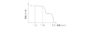
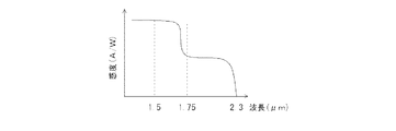
- FIG. 2 is a diagram showing the wavelength dependence of the sensitivity of the light receiving element 10 shown in FIG. From the above (1) to (3), it can be seen that the sensitivity at a wavelength of 1.5 ⁇ m to 1.75 ⁇ m is at a high level in a substantially flat state continuously from the sensitivity on the shorter wavelength side.
- the upper limit of the receivable wavelength is about 2.3 ⁇ m.
- FIG. 3 shows a piping system and the like of the film formation apparatus 60 of the all-organic metal vapor phase epitaxy method.
- a quartz tube 65 is disposed in the reaction chamber (chamber) 63, and a raw material gas is introduced into the quartz tube 65.
- a substrate table 66 is disposed in the quartz tube 65 so as to be rotatable and airtight.
- the substrate table 66 is provided with a heater 66h for heating the substrate.
- the temperature of the surface of the wafer 50 a during film formation is monitored by the infrared temperature monitor device 61 through a window 69 provided in the ceiling of the reaction chamber 63. This monitored temperature is a temperature at the time of growth or a temperature called a film forming temperature or a substrate temperature.
- 600 ° C. or lower is a temperature measured by this temperature monitor.
- the forced exhaust from the quartz tube 65 is performed by a vacuum pump.
- the source gas is supplied by a pipe communicating with the quartz tube 65.
- the all-organometallic vapor phase growth method is characterized in that all source gases are supplied in the form of an organometallic gas.
- source gases such as impurities are not specified, but impurities are also introduced in the form of an organometallic gas.
- the raw material of the organometallic gas is put in a thermostat and kept at a constant temperature. Hydrogen (H 2 ) and nitrogen (N 2 ) are used as the carrier gas.
- the organometallic gas is transported by a transport gas, and is sucked by a vacuum pump and introduced into the quartz tube 65.
- the amount of carrier gas is accurately adjusted by an MFC (Mass Flow Controller). Many flow controllers, electromagnetic valves, and the like are automatically controlled by a microcomputer.
- MFC Mass Flow Controller
- the crystallinity of the InP substrate located in the lower layer is not deteriorated by heating at about 600 ° C.
- the substrate temperature is strictly maintained, for example, in the range of 400 ° C. or more and 600 ° C. or less. There is a need to. The reason is that when heated above 600 ° C., GaAs 0.57 Sb 0.43 is damaged by heat and crystallinity is greatly deteriorated, and when an InP window layer is formed at a temperature lower than 400 ° C.
- the buffer layer 2 may be an InP layer alone, but in a predetermined case, an n-type doped In 0.53 Ga 0.47 As layer is formed on the InP buffer layer with a thickness of 0.15 ⁇ m (150 nm). You may grow into. This In 0.53 Ga 0.47 As layer is also included in the buffer layer 2 in FIG.
- a type 2 MQW light-receiving layer 3 having In 0.59 Ga 0.41 As3a / GaAs 0.57 Sb 0.43 3b as a pair of quantum wells is formed.
- the film thicknesses of In 0.59 Ga 0.41 As3a and GaAs 0.57 Sb 0.43 3b in the quantum well are 1 nm or more and 10 nm or less.
- the MQW light-receiving layer 3 is formed by stacking 200 pairs of quantum wells.
- triethylgallium (TEGa), tertiary butylarsine (TBAs) and trimethylantimony (TMSb) are used.
- TEGa, TMIn, and TBAs can be used.
- These source gases are all organometallic gases, and the molecular weight of the compound is large. Therefore, it can be completely decomposed at a relatively low temperature of 400 ° C. or higher and 600 ° C. or lower and contribute to crystal growth.
- the temperature difference from the film formation temperature to room temperature can be reduced, the strain caused by the difference in thermal expansion of each material in the light receiving element 10 can be reduced, and the lattice defect density can be reduced. This is effective in suppressing dark current.
- the raw material for Ga (gallium) may be TEGa (triethylgallium) or TMGa (trimethylgallium).
- the raw material for In (indium) may be TMIn (trimethylindium) or TEIn (triethylindium).
- As (arsenic) TBAs (tertiary butylarsine) or TMAs (trimethylarsenic) may be used.
- Sb (antimony) may be TMSb (trimethylantimony), TESb (triethylantimony), TIPSb (triisopropylantimony), or TDMASb (tridimethylaminoantimony).
- a semiconductor element having a low MQW impurity concentration and excellent crystallinity can be obtained.
- a light receiving element with a small dark current and a high sensitivity can be obtained. Furthermore, it is possible to capture a clear image even with weak light using the light receiving element.
- the source gas is transported through the piping, introduced into the quartz tube 65, and exhausted. Any number of source gases can be supplied to the quartz tube 65 by increasing the number of pipes. For example, even a dozen kinds of source gases are controlled by opening and closing the electromagnetic valve.
- the flow rate of the source gas is controlled by a flow rate controller (MFC) shown in FIG. 3, and the flow into the quartz tube 65 is turned on and off by opening and closing the electromagnetic valve.
- MFC flow rate controller
- the quartz tube 65 is forcibly exhausted by a vacuum pump. There is no stagnation in the flow of the source gas, and it is performed smoothly and automatically. Therefore, the composition is switched quickly when forming the quantum well pair.
- the temperature distribution of the source gas does not have the directivity as on the inflow side or the outlet side of the source gas.
- the wafer 50a revolves on the substrate table 66, the flow of the source gas near the surface of the wafer 50a is in a turbulent state, and even the source gas near the surface of the wafer 50a contacts the wafer 50a. Except for the raw material gas, it has a large velocity component in the flow direction from the introduction side to the exhaust side. Therefore, most of the heat flowing from the substrate table 66 to the source gas through the wafer 50a is always exhausted together with the exhaust gas.
- the substrate temperature is heated to a low temperature range of 400 ° C. or more and 600 ° C. or less.
- the decomposition efficiency of the raw material is good, so that multiple quantum wells with the raw material gas flowing in a range very close to the wafer 50a
- the source gas that contributes to the growth of the structure is limited to one that is efficiently decomposed into the shape necessary for growth.
- the surface of the wafer 50a is set to a monitored temperature.
- the temperature suddenly decreases or a large temperature step is generated as described above. Therefore, in the case of a raw material gas having a decomposition temperature of T1 ° C., the substrate surface temperature is set to (T1 + ⁇ ), and ⁇ is determined in consideration of variations in temperature distribution and the like.
- T1 + ⁇ the substrate surface temperature
- ⁇ is determined in consideration of variations in temperature distribution and the like.
- the range is limited to the range of the thickness of the organic metal molecules corresponding to several from the surface. Therefore, organometallic molecules in the range in contact with the wafer surface and molecules located within the film thickness range of several organometallic molecules from the wafer surface mainly contribute to the crystal growth, and the outer organic molecules. It is considered that the metal molecules are discharged out of the quartz tube 65 with almost no decomposition. When the organometallic molecules near the surface of the wafer 50a are decomposed and crystal growth occurs, the organometallic molecules located outside enter the replenishment.
- the range of the organometallic molecules that can participate in crystal growth is limited to a thin source gas layer on the surface of the wafer 50a by making the wafer surface temperature slightly higher than the temperature at which the organometallic molecules decompose. it can.
- phase separation occurs in the GaAsSb layer of the multiple quantum well structure when grown in a temperature range exceeding 600 ° C., and the crystal growth surface of the multiple quantum well structure that is clean and excellent in flatness, and A multiple quantum well structure having excellent periodicity and crystallinity cannot be obtained.
- the growth temperature is set to a temperature range of 400 ° C. or more and 600 ° C. or less.
- this film-forming method is an all-organic MOVPE method and all the source gases are made into organometallic gases with high decomposition efficiency. is there.
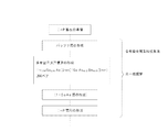
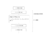
- FIG. 4 is a flowchart of a method for manufacturing a light receiving element.
- an In 0.53 Ga 0.47 As diffusion concentration distribution adjusting layer 4 lattice-matched to InP is located on the type 2 MQW light receiving layer 3, and the In 0.53
- the InP window layer 5 is located on the Ga 0.47 As diffusion concentration distribution adjusting layer 4.
- the p-type region 6 is provided by selectively diffusing Zn of the p-type impurity from the opening of the selective diffusion mask pattern 36 provided on the surface of the InP window layer 5.
- a pn junction or a pi junction is formed at the tip of the p-type region 6.
- a reverse bias voltage is applied to the pn junction or pi junction to form a depletion layer, and the charge due to photoelectron conversion is captured, so that the brightness of the pixel corresponds to the amount of charge.
- the p-type region 6 or the pn junction or pi junction is the main part constituting the pixel.
- the p-side electrode 11 that is in ohmic contact with the p-type region 6 is a pixel electrode, and reads the above charges for each pixel with the n-side electrode 12 that is set to the ground potential.
- the selective diffusion mask pattern 36 is left as it is on the surface of the InP window layer around the p-type region 6. Further, a protective film such as SiON not shown is coated. The selective diffusion mask pattern 36 is left as it is.
- the interfaces 16 and 17 are not regrowth interfaces. Therefore, at the interfaces 16 and 17 of the light receiving element 10 shown in FIG. 1, the oxygen and carbon concentrations are both below 1 ⁇ 10 17 cm ⁇ 3 and below a predetermined level, and in particular, the p-type region 6 and the interface 17 No charge leakage occurs at the intersection line. Also, the lattice defect density can be kept low at the interface 16.
- a non-doped In 0.53 Ga 0.47 As diffusion concentration distribution layer 4 having a film thickness of 1.0 ⁇ m, for example, is formed on the MQW light-receiving layer 3.
- the In 0.53 Ga 0.47 As diffusion concentration distribution layer 4 allows Zn of p-type impurities to reach the MQW light-receiving layer 3 from the InP window layer 5 by a selective diffusion method.
- the In 0.53 Ga 0.47 As diffusion concentration distribution adjusting layer 4 may be arranged as described above, but may not be provided.
- a p-type region 6 is formed by the selective diffusion described above, and a pn junction or a pi junction is formed at the tip thereof. Even when the In 0.53 Ga 0.47 As diffusion concentration distribution adjusting layer 4 is inserted, since the band gap of In 0.53 Ga 0.47 As is small, the electric resistance of the light receiving element is reduced even if it is non-doped. Can be lowered. By reducing the electrical resistance, it is possible to improve the responsiveness and obtain a moving image with good image quality. On the In 0.53 Ga 0.47 As diffusion concentration distribution adjusting layer 4, the undoped InP window layer 5 is continuously formed by the all-organic metal vapor phase epitaxy method while the wafer 50 a is disposed in the same quartz tube 65.
- the growth temperature of the InP window layer 5 can be made 400 ° C. or more and 600 ° C. or less, and further 550 ° C. or less.
- the MQW GaAsSb located under the InP window layer 5 is not damaged by heat, and the MQW crystallinity is not impaired.
- the interface between the In 0.53 Ga 0.47 As diffusion concentration distribution adjusting layer and the InP window layer was a regrowth interface once exposed to the atmosphere.
- the regrowth interface is identified by satisfying at least one of the oxygen concentration of 1 ⁇ 10 17 cm ⁇ 3 or more and the carbon concentration of 1 ⁇ 10 17 cm ⁇ 3 or more by secondary ion mass spectrometry. Can do.
- the regrowth interface forms a crossing line with the p-type region, and a charge leak occurs at the crossing line, thereby significantly degrading the image quality.
- MOVPE method total organic MOCVD not
- the decomposition temperature is high, GaAs 0 located in the lower layer .57 Sb 0.43 heat damage is induced and the MQW crystallinity is impaired .
- the same film formation chamber or quartz tube 65 is consistently used until the growth temperature is lowered by using only the organometallic gas as the source gas and the formation of the InP window layer 5 is completed. It has no recrystallization interface. As a result, it is possible to efficiently and efficiently manufacture a large number of photodiodes having low charge leakage, excellent crystallinity, and light receiving sensitivity in a wavelength region of 1.5 ⁇ m to 1.8 ⁇ m.
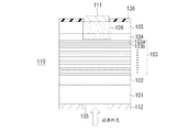
- FIG. 5 is a cross-sectional view of a light receiving element 110 shown as a reference example.
- the laminated structure is similar to the light receiving element 10 of the embodiment of the present invention shown in FIG. That is, (light-receiving layer 103 / In 0.53 Ga 0.47 As having a multiple quantum well structure of (InP substrate 101 / InP buffer layer 102 / In 0.53 Ga 0.47 As and GaAs 0.51 Sb 0.49) It has a laminated structure of diffusion concentration distribution adjusting layer 104 / InP window layer 105).
- the light receiving layer 103 is formed by stacking 200 pairs of quantum wells.
- the In 0.53 Ga 0.47 As layer 103a and the GaAs 0.51 Sb 0.49 layer 103b constituting the light receiving layer 103 both have a composition lattice-matched to InP. That is.
- a multiple quantum well structure is formed by (In 0.53 Ga 0.47 As layer 103a / GaAs 0.51 Sb 0.49 layer 103b) having a composition lattice-matched to InP.
- the conventional type 2 multiple quantum well structure of In 0.53 Ga 0.47 As and GaAs 0.51 Sb 0.49 is, without exception, a multiple quantum well structure having a lattice matching composition as shown in FIG. Was used.
- FIG. 6 is a diagram showing the wavelength dependence of the sensitivity of the light receiving element 110 shown in FIG.
- the wavelength upper limit of the light receiving sensitivity is up to 2.3 ⁇ m reflecting the type 2 multiple quantum well structure of In 0.53 Ga 0.47 As and GaAs 0.51 Sb 0.49 .
- the sensitivity rapidly decreases on the long wavelength side. This poses a problem in performing a highly reliable analysis using a plurality of absorption bands concentrated at wavelengths of 1.5 ⁇ m to 1.75 ⁇ m.
- FIG. 7 is a diagram showing the light receiving element 10 according to Embodiment 2 of the present invention.
- a pixel is formed by selectively diffusing zinc (Zn), which is a p-type impurity, from the InP window layer 5.
- the distribution of the selectively diffused Zn is from 1 ⁇ 10 18 cm ⁇ 3 to 1 ⁇ 10 19 cm ⁇ 3 on the InP window layer 5 side in the In 0.53 Ga 0.47 As diffusion concentration distribution adjusting layer 4.
- the above laminated structure is configured based on the following concept. 1. In 0.59 Ga 0.41 As3a (first semiconductor layer) in the light-receiving layer 3 The In composition x is set to 0.59 so that the band gap can be made as small as possible to receive light having a long wavelength. As a result, the upper limit of the light receiving area can be expanded to a wavelength of about 1800 nm. However, In 0.59 Ga 0.41 As3a has a large lattice constant, and by itself, it is difficult to lattice match with InP. As a result, dark current increases as the lattice defect density increases, making it difficult to detect weak light with sufficient resolution.
- the lattice defect density in the diffusion concentration distribution adjusting layer 4 and the window layer 5 grown on and in contact with the light receiving layer 3 is not increased, and the In 0.53 Ga 0.47 As diffusion concentration distribution having a good surface property.
- the adjustment layer 4 / InP window layer 5 is formed, and the dark current does not increase.
- (2) The vicinity of the upper limit wavelength (1800 nm) of the light receiving wavelength range is left to the above-described first semiconductor, In 0.59 Ga 0.41 As3a, and light corresponding to energy having a larger band gap is received.
- the first semiconductor In 0.59 Ga 0.41 As3a itself receives not only light near the upper limit of the long wavelength but also light on the shorter wavelength side.
- FIG. 8 is a diagram showing the wavelength dependence of the sensitivity of the light receiving element 10 shown in FIG. From the above (1) to (2), it can be seen that the sensitivity at the wavelength of 1.5 ⁇ m to 1.75 ⁇ m is at a high level in a substantially flat state continuously from the sensitivity on the shorter wavelength side.
- type 2 transition does not occur, and the upper limit of the wavelength at which light can be received is determined by the type 1 transition of the first semiconductor In 0.59 Ga 0.41 As3a.
- FIG. 9 is a diagram showing a flowchart of a manufacturing method of the light receiving element 10 shown in FIG.
- the multiple quantum well structure is formed by In 0.59 Ga 0.41 As3a and In 0.47 Ga 0.53 As3c, except that it is different from the first embodiment, and the other is the same as the first embodiment. .
- Example 1 A light-receiving element corresponding to the first embodiment was prototyped, and the light-receiving sensitivity and the dark current at wavelengths of 1.5 ⁇ m and 1.75 ⁇ m were evaluated.
- the test specimens are eight specimens A1 to A8 shown in Table 1. Among these test specimens, specimens A3 to A7 are examples of the present invention, and specimens A1, A2, and A8 are comparative examples.
- the first semiconductor layer 3a was made of In 0.59 Ga 0.41 As
- the second semiconductor layer 3b was made of GaAs 0.57 Sb 0.43 .
- the thickness structure is as follows.
- the light receiving sensitivity at each wavelength was measured at room temperature by the photocurrent generated when white light was incident from the back surface of the substrate through a bandpass filter corresponding to each wavelength.
- the dark current was measured at room temperature from the current flowing when no light was irradiated.
- 10 mA / cm 2 or more was regarded as defective (x), and less than 10 mA / cm 2 was evaluated as good ( ⁇ ).
- the ratio between the sensitivity of the wavelength of 1.5 ⁇ m and the sensitivity of 1.75 ⁇ m was 0.8 or more, and each sensitivity itself was 0.20 A / W or more.
- a case where the above sensitivity ratio was less than 0.8 was regarded as defective (x).
- a specimen that did not contain a defect (x) in both dark current and sensitivity was rated as good overall judgment ( ⁇ ). In particular, the case where the sensitivity itself was 1.0 A / W or higher was evaluated as excellent (().
- the sensitivity ratio was 0.8 or more, and the evaluation of dark current was good.
- Inventive Example A6 was excellent in both sensitivity and dark current, and excellent ( ⁇ ) was obtained in comprehensive judgment.
- the sensitivity ratio was poor in Comparative Example A1.
- Comparative Example A2 the sensitivity itself was low and the dark current was large.
- Comparative Example A8 the sensitivity at wavelengths of 1.5 ⁇ m and 1.75 ⁇ m was good, but the dark current was very large.
- Example 2 A light-receiving element corresponding to the second embodiment was prototyped, and the light-receiving sensitivity and dark current at wavelengths of 1.5 ⁇ m and 1.75 ⁇ m were evaluated.
- the test bodies are eight test bodies B1 to B8 shown in Table 2.
- test bodies B3 to B7 are examples of the present invention
- test bodies B1, B2, and B8 are comparative examples.
- the first semiconductor layer 3a was made of In 0.59 Ga 0.41 As
- the second semiconductor layer 3c was made of In 0.47 Ga 0.53 As.
- the thickness structure is as follows.
- Example B3 (1 nm / 1 nm) ⁇ 250 pairs: light receiving layer thickness 0.5 ⁇ m
- Example B4 (5 nm / 5 nm) ⁇ 50 pairs: light receiving layer thickness 0.5 ⁇ m
- Example B5 (5 nm / 5 nm) ⁇ 100 pair: light receiving layer thickness 1.0 ⁇ m
- Example B6 (5 nm / 5 nm) ⁇ 200 pairs: light receiving layer thickness 2.0 ⁇ m
- Example B7 (10 nm / 10 nm) ⁇ 100 pair: light receiving layer thickness 2.0 ⁇ m
- Comparative Example B1 (5 nm / 5 nm) ⁇ 40 pair: light receiving layer thickness 0.4 ⁇ m
- Comparative Example B2 (0.5 nm / 0.5 nm) ⁇ 500 pair: light receiving layer thickness 0.5 ⁇ m Comparative Example B8: (20 nm / 20 nm) ⁇ 50 pairs: light receiving layer thickness 2.0 ⁇ m In the test, light receiving sensitivity
- the dark current 10 mA / cm 2 or more was judged as poor (x), and less than 10 mA / cm 2 was judged as good ( ⁇ ).
- the ratio between the sensitivity of the wavelength of 1.5 ⁇ m and the sensitivity of 1.75 ⁇ m was 0.8 or more, and each sensitivity itself was 0.20 A / W or more.
- a case where the above sensitivity ratio was less than 0.8 was regarded as defective (x).
- a specimen that did not contain a defect (x) in both dark current and sensitivity was rated as good overall judgment ( ⁇ ). In particular, the case where the sensitivity itself was 1.0 A / W or higher was evaluated as excellent (().
- the above sensitivity ratio in Invention Examples B3 to B7 was 0.8 or more, and the evaluation of dark current was also good.
- sample B6 excellent evaluation was obtained in both sensitivity and dark current, and excellent ()) was obtained in the comprehensive judgment.
- the sensitivity ratio was poor in Comparative Example B1.
- Comparative Example B2 the sensitivity itself was poor and the dark current was large.
- Comparative Example B8 the sensitivity at wavelengths of 1.5 ⁇ m and 1.75 ⁇ m was good, but the dark current was very large.
- the dark current can be lowered with a sufficiently high sensitivity in the near infrared wavelength range of 1.5 ⁇ m to 1.8 ⁇ m. For this reason, a clear image can be obtained despite a small amount of light, and it can be suitably used for a wide range of applications as well as for communication and night imaging.
Landscapes
- Chemical & Material Sciences (AREA)
- Engineering & Computer Science (AREA)
- Crystallography & Structural Chemistry (AREA)
- Organic Chemistry (AREA)
- Materials Engineering (AREA)
- Metallurgy (AREA)
- Inorganic Chemistry (AREA)
- Nanotechnology (AREA)
- Chemical Kinetics & Catalysis (AREA)
- General Chemical & Material Sciences (AREA)
- Physics & Mathematics (AREA)
- Life Sciences & Earth Sciences (AREA)
- Biophysics (AREA)
- Optics & Photonics (AREA)
- Light Receiving Elements (AREA)
Abstract
L'invention concerne un élément photorécepteur ou similaire qui offre une sensibilité suffisamment élevée dans la région de longueur d'onde de l'infrarouge proche de 1,5 à 1,8 µm et qui est en mesure de réduire le courant d'obscurité. Un élément photorécepteur (10) selon l'invention comprend une couche tampon (2) disposée adjacente sur le dessus d'un substrat d'InP (1) et une couche photoréceptrice (3) disposée adjacente sur le dessus de la couche tampon. La couche photoréceptrice est formée d'au moins 50 paires, une paire étant une première couche semi-conductrice (3a) ayant une bande interdite de 0,73 eV ou moins et une seconde couche semi-conductrice (3b) ayant une bande interdite supérieure à celle de la première couche semi-conductrice. La première couche semi-conductrice (3a) et la seconde couche semi-conductrice (3b) forment une structure de puits quantique à compensation des contraintes et l'épaisseur de chaque couche est comprise entre 1 nm et 10 nm.
Priority Applications (2)
| Application Number | Priority Date | Filing Date | Title |
|---|---|---|---|
| CN2012800100225A CN103403884A (zh) | 2011-02-23 | 2012-02-03 | 光接收元件及其制造方法 |
| US14/000,187 US20130313521A1 (en) | 2011-02-23 | 2012-02-03 | Photodiode and method for producing the same |
Applications Claiming Priority (2)
| Application Number | Priority Date | Filing Date | Title |
|---|---|---|---|
| JP2011037182A JP2012174977A (ja) | 2011-02-23 | 2011-02-23 | 受光素子およびその製造方法 |
| JP2011-037182 | 2011-02-23 |
Publications (1)
| Publication Number | Publication Date |
|---|---|
| WO2012114849A1 true WO2012114849A1 (fr) | 2012-08-30 |
Family
ID=46720637
Family Applications (1)
| Application Number | Title | Priority Date | Filing Date |
|---|---|---|---|
| PCT/JP2012/052478 Ceased WO2012114849A1 (fr) | 2011-02-23 | 2012-02-03 | Élément photorécepteur et son procédé de fabrication |
Country Status (5)
| Country | Link |
|---|---|
| US (1) | US20130313521A1 (fr) |
| JP (1) | JP2012174977A (fr) |
| CN (1) | CN103403884A (fr) |
| TW (1) | TW201251090A (fr) |
| WO (1) | WO2012114849A1 (fr) |
Cited By (3)
| Publication number | Priority date | Publication date | Assignee | Title |
|---|---|---|---|---|
| JP2014216624A (ja) * | 2013-04-30 | 2014-11-17 | 住友電気工業株式会社 | エピタキシャルウエハ、その製造方法、半導体素子、および光学センサ装置 |
| US20150162471A1 (en) * | 2012-06-28 | 2015-06-11 | Elta Systems Ltd. | Phototransistor device |
| WO2019044686A1 (fr) * | 2017-09-01 | 2019-03-07 | 住友電気工業株式会社 | Stratifié semi-conducteur, élément de réception de lumière et procédé de fabrication de stratifié semi-conducteur |
Families Citing this family (8)
| Publication number | Priority date | Publication date | Assignee | Title |
|---|---|---|---|---|
| CN102881760B (zh) * | 2012-10-08 | 2016-12-28 | 上海集成电路研发中心有限公司 | 红外感测器及其制造方法 |
| JP6115890B2 (ja) * | 2013-09-13 | 2017-04-19 | 住友電気工業株式会社 | 受光素子、その製造方法、および光センサ装置 |
| JP2015149335A (ja) * | 2014-02-05 | 2015-08-20 | 住友電気工業株式会社 | 半導体積層体、半導体積層体の製造方法および半導体装置の製造方法 |
| JP2015225886A (ja) * | 2014-05-26 | 2015-12-14 | 日本放送協会 | 光電変換素子、光電変換素子の製造方法、積層型固体撮像素子および太陽電池 |
| WO2016171009A1 (fr) * | 2015-04-22 | 2016-10-27 | 住友電気工業株式会社 | Stratifié semi-conducteur, élément de réception de lumière et procédé de fabrication de stratifié semi-conducteur |
| JP6488855B2 (ja) * | 2015-04-22 | 2019-03-27 | 住友電気工業株式会社 | 半導体積層体、受光素子および半導体積層体の製造方法 |
| JP6589662B2 (ja) * | 2016-01-27 | 2019-10-16 | 住友電気工業株式会社 | 半導体積層体および受光素子 |
| JP6613923B2 (ja) * | 2016-01-27 | 2019-12-04 | 住友電気工業株式会社 | 半導体積層体、受光素子および半導体積層体の製造方法 |
Citations (9)
| Publication number | Priority date | Publication date | Assignee | Title |
|---|---|---|---|---|
| JPH0461174A (ja) * | 1990-06-22 | 1992-02-27 | Nec Corp | アバランシェフォトダイオード |
| JPH06188449A (ja) * | 1992-12-21 | 1994-07-08 | Furukawa Electric Co Ltd:The | Msm型受光素子 |
| JPH0774381A (ja) * | 1993-09-01 | 1995-03-17 | Mitsubishi Electric Corp | 半導体受光素子 |
| JPH09219563A (ja) * | 1996-02-09 | 1997-08-19 | Hitachi Ltd | 半導体光素子とそれを用いた応用システム |
| JP2002064217A (ja) * | 2000-06-06 | 2002-02-28 | Fujitsu Quantum Devices Ltd | 半導体受光装置およびその製造方法 |
| JP2008153311A (ja) * | 2006-12-14 | 2008-07-03 | Sumitomo Electric Ind Ltd | 半導体受光素子、視界支援装置および生体医療装置 |
| JP2008288293A (ja) * | 2007-05-16 | 2008-11-27 | Nippon Telegr & Teleph Corp <Ntt> | 半導体受光素子 |
| WO2010073768A1 (fr) * | 2008-12-26 | 2010-07-01 | 住友電気工業株式会社 | Élément de réception de lumière, réseau d'éléments de réception de lumière, procédé de fabrication d'élément de réception de lumière et procédé de fabrication de réseau d'éléments de réception de lumière |
| WO2011016309A1 (fr) * | 2009-08-01 | 2011-02-10 | 住友電気工業株式会社 | Élément semi-conducteur et procédé pour sa fabrication |
Family Cites Families (4)
| Publication number | Priority date | Publication date | Assignee | Title |
|---|---|---|---|---|
| GB0118150D0 (en) * | 2001-07-25 | 2001-09-19 | Imperial College | Thermophotovoltaic device |
| JP5262293B2 (ja) * | 2008-05-26 | 2013-08-14 | 三菱電機株式会社 | 光半導体装置 |
| JP5422990B2 (ja) * | 2008-12-22 | 2014-02-19 | 住友電気工業株式会社 | 生体成分検出装置 |
| JP4840451B2 (ja) * | 2009-01-22 | 2011-12-21 | 住友電気工業株式会社 | 近赤外イメージセンサ |
-
2011
- 2011-02-23 JP JP2011037182A patent/JP2012174977A/ja active Pending
-
2012
- 2012-02-03 WO PCT/JP2012/052478 patent/WO2012114849A1/fr not_active Ceased
- 2012-02-03 CN CN2012800100225A patent/CN103403884A/zh active Pending
- 2012-02-03 US US14/000,187 patent/US20130313521A1/en not_active Abandoned
- 2012-02-14 TW TW101104799A patent/TW201251090A/zh unknown
Patent Citations (9)
| Publication number | Priority date | Publication date | Assignee | Title |
|---|---|---|---|---|
| JPH0461174A (ja) * | 1990-06-22 | 1992-02-27 | Nec Corp | アバランシェフォトダイオード |
| JPH06188449A (ja) * | 1992-12-21 | 1994-07-08 | Furukawa Electric Co Ltd:The | Msm型受光素子 |
| JPH0774381A (ja) * | 1993-09-01 | 1995-03-17 | Mitsubishi Electric Corp | 半導体受光素子 |
| JPH09219563A (ja) * | 1996-02-09 | 1997-08-19 | Hitachi Ltd | 半導体光素子とそれを用いた応用システム |
| JP2002064217A (ja) * | 2000-06-06 | 2002-02-28 | Fujitsu Quantum Devices Ltd | 半導体受光装置およびその製造方法 |
| JP2008153311A (ja) * | 2006-12-14 | 2008-07-03 | Sumitomo Electric Ind Ltd | 半導体受光素子、視界支援装置および生体医療装置 |
| JP2008288293A (ja) * | 2007-05-16 | 2008-11-27 | Nippon Telegr & Teleph Corp <Ntt> | 半導体受光素子 |
| WO2010073768A1 (fr) * | 2008-12-26 | 2010-07-01 | 住友電気工業株式会社 | Élément de réception de lumière, réseau d'éléments de réception de lumière, procédé de fabrication d'élément de réception de lumière et procédé de fabrication de réseau d'éléments de réception de lumière |
| WO2011016309A1 (fr) * | 2009-08-01 | 2011-02-10 | 住友電気工業株式会社 | Élément semi-conducteur et procédé pour sa fabrication |
Cited By (7)
| Publication number | Priority date | Publication date | Assignee | Title |
|---|---|---|---|---|
| US20150162471A1 (en) * | 2012-06-28 | 2015-06-11 | Elta Systems Ltd. | Phototransistor device |
| JP2014216624A (ja) * | 2013-04-30 | 2014-11-17 | 住友電気工業株式会社 | エピタキシャルウエハ、その製造方法、半導体素子、および光学センサ装置 |
| US9698287B2 (en) | 2013-04-30 | 2017-07-04 | Sumitomo Electric Industries, Ltd. | Epitaxial wafer, method for producing the same, semiconductor element, and optical sensor device |
| WO2019044686A1 (fr) * | 2017-09-01 | 2019-03-07 | 住友電気工業株式会社 | Stratifié semi-conducteur, élément de réception de lumière et procédé de fabrication de stratifié semi-conducteur |
| JPWO2019044686A1 (ja) * | 2017-09-01 | 2020-08-27 | 住友電気工業株式会社 | 半導体積層体、受光素子および半導体積層体の製造方法 |
| US11081605B2 (en) | 2017-09-01 | 2021-08-03 | Sumitomo Electric Industries, Ltd. | Semiconductor laminate, light-receiving element, and method for manufacturing semiconductor laminate |
| JP7078049B2 (ja) | 2017-09-01 | 2022-05-31 | 住友電気工業株式会社 | 半導体積層体、受光素子および半導体積層体の製造方法 |
Also Published As
| Publication number | Publication date |
|---|---|
| TW201251090A (en) | 2012-12-16 |
| JP2012174977A (ja) | 2012-09-10 |
| CN103403884A (zh) | 2013-11-20 |
| US20130313521A1 (en) | 2013-11-28 |
Similar Documents
| Publication | Publication Date | Title |
|---|---|---|
| JP5649157B2 (ja) | 半導体素子およびその製造方法 | |
| WO2012114849A1 (fr) | Élément photorécepteur et son procédé de fabrication | |
| US9818895B2 (en) | Semiconductor device, optical sensor device and semiconductor device manufacturing method | |
| US9129808B2 (en) | Epitaxial wafer, photodiode, optical sensor device, and methods for producing epitaxial wafer and photodiode | |
| JP5736922B2 (ja) | 受光素子およびその製造方法 | |
| US8822977B2 (en) | Photodetector and method of manufacturing the photodetector | |
| US9190544B2 (en) | Photodiode, optical sensor device, and photodiode manufacturing method | |
| JP6036906B2 (ja) | 受光素子およびその製造方法 | |
| JP5593846B2 (ja) | 受光素子、光学センサ装置および受光素子の製造方法 | |
| JP5776715B2 (ja) | 半導体素子、光学センサ装置および半導体素子の製造方法 | |
| JP2015015476A (ja) | エピタキシャルウェハおよびその製造方法 |
Legal Events
| Date | Code | Title | Description |
|---|---|---|---|
| 121 | Ep: the epo has been informed by wipo that ep was designated in this application |
Ref document number: 12749020 Country of ref document: EP Kind code of ref document: A1 |
|
| WWE | Wipo information: entry into national phase |
Ref document number: 14000187 Country of ref document: US |
|
| NENP | Non-entry into the national phase |
Ref country code: DE |
|
| 122 | Ep: pct application non-entry in european phase |
Ref document number: 12749020 Country of ref document: EP Kind code of ref document: A1 |