WO2012121332A1 - Oxyde pour couche semi-conductrice pour transistor à couche mince, couche semi-conductrice pour transistor à couche mince comprenant ledit oxyde et transistor à couche mince - Google Patents
Oxyde pour couche semi-conductrice pour transistor à couche mince, couche semi-conductrice pour transistor à couche mince comprenant ledit oxyde et transistor à couche mince Download PDFInfo
- Publication number
- WO2012121332A1 WO2012121332A1 PCT/JP2012/055966 JP2012055966W WO2012121332A1 WO 2012121332 A1 WO2012121332 A1 WO 2012121332A1 JP 2012055966 W JP2012055966 W JP 2012055966W WO 2012121332 A1 WO2012121332 A1 WO 2012121332A1
- Authority
- WO
- WIPO (PCT)
- Prior art keywords
- thin film
- semiconductor layer
- oxide
- sputtering
- film transistor
- Prior art date
- Legal status (The legal status is an assumption and is not a legal conclusion. Google has not performed a legal analysis and makes no representation as to the accuracy of the status listed.)
- Ceased
Links
Images






Classifications
-
- H—ELECTRICITY
- H10—SEMICONDUCTOR DEVICES; ELECTRIC SOLID-STATE DEVICES NOT OTHERWISE PROVIDED FOR
- H10P—GENERIC PROCESSES OR APPARATUS FOR THE MANUFACTURE OR TREATMENT OF DEVICES COVERED BY CLASS H10
- H10P14/00—Formation of materials, e.g. in the shape of layers or pillars
- H10P14/20—Formation of materials, e.g. in the shape of layers or pillars of semiconductor materials
- H10P14/34—Deposited materials, e.g. layers
- H10P14/3402—Deposited materials, e.g. layers characterised by the chemical composition
- H10P14/3424—Deposited materials, e.g. layers characterised by the chemical composition being Group IIB-VIA materials
- H10P14/3426—Oxides
-
- G—PHYSICS
- G02—OPTICS
- G02F—OPTICAL DEVICES OR ARRANGEMENTS FOR THE CONTROL OF LIGHT BY MODIFICATION OF THE OPTICAL PROPERTIES OF THE MEDIA OF THE ELEMENTS INVOLVED THEREIN; NON-LINEAR OPTICS; FREQUENCY-CHANGING OF LIGHT; OPTICAL LOGIC ELEMENTS; OPTICAL ANALOGUE/DIGITAL CONVERTERS
- G02F1/00—Devices or arrangements for the control of the intensity, colour, phase, polarisation or direction of light arriving from an independent light source, e.g. switching, gating or modulating; Non-linear optics
- G02F1/01—Devices or arrangements for the control of the intensity, colour, phase, polarisation or direction of light arriving from an independent light source, e.g. switching, gating or modulating; Non-linear optics for the control of the intensity, phase, polarisation or colour
- G02F1/13—Devices or arrangements for the control of the intensity, colour, phase, polarisation or direction of light arriving from an independent light source, e.g. switching, gating or modulating; Non-linear optics for the control of the intensity, phase, polarisation or colour based on liquid crystals, e.g. single liquid crystal display cells
- G02F1/133—Constructional arrangements; Operation of liquid crystal cells; Circuit arrangements
- G02F1/136—Liquid crystal cells structurally associated with a semi-conducting layer or substrate, e.g. cells forming part of an integrated circuit
- G02F1/1362—Active matrix addressed cells
- G02F1/1368—Active matrix addressed cells in which the switching element is a three-electrode device
-
- H—ELECTRICITY
- H10—SEMICONDUCTOR DEVICES; ELECTRIC SOLID-STATE DEVICES NOT OTHERWISE PROVIDED FOR
- H10D—INORGANIC ELECTRIC SEMICONDUCTOR DEVICES
- H10D30/00—Field-effect transistors [FET]
- H10D30/01—Manufacture or treatment
- H10D30/021—Manufacture or treatment of FETs having insulated gates [IGFET]
- H10D30/031—Manufacture or treatment of FETs having insulated gates [IGFET] of thin-film transistors [TFT]
-
- H—ELECTRICITY
- H10—SEMICONDUCTOR DEVICES; ELECTRIC SOLID-STATE DEVICES NOT OTHERWISE PROVIDED FOR
- H10D—INORGANIC ELECTRIC SEMICONDUCTOR DEVICES
- H10D30/00—Field-effect transistors [FET]
- H10D30/60—Insulated-gate field-effect transistors [IGFET]
- H10D30/67—Thin-film transistors [TFT]
- H10D30/674—Thin-film transistors [TFT] characterised by the active materials
- H10D30/6755—Oxide semiconductors, e.g. zinc oxide, copper aluminium oxide or cadmium stannate
-
- H—ELECTRICITY
- H10—SEMICONDUCTOR DEVICES; ELECTRIC SOLID-STATE DEVICES NOT OTHERWISE PROVIDED FOR
- H10D—INORGANIC ELECTRIC SEMICONDUCTOR DEVICES
- H10D62/00—Semiconductor bodies, or regions thereof, of devices having potential barriers
- H10D62/10—Shapes, relative sizes or dispositions of the regions of the semiconductor bodies; Shapes of the semiconductor bodies
-
- H—ELECTRICITY
- H10—SEMICONDUCTOR DEVICES; ELECTRIC SOLID-STATE DEVICES NOT OTHERWISE PROVIDED FOR
- H10D—INORGANIC ELECTRIC SEMICONDUCTOR DEVICES
- H10D62/00—Semiconductor bodies, or regions thereof, of devices having potential barriers
- H10D62/80—Semiconductor bodies, or regions thereof, of devices having potential barriers characterised by the materials
-
- H—ELECTRICITY
- H10—SEMICONDUCTOR DEVICES; ELECTRIC SOLID-STATE DEVICES NOT OTHERWISE PROVIDED FOR
- H10D—INORGANIC ELECTRIC SEMICONDUCTOR DEVICES
- H10D62/00—Semiconductor bodies, or regions thereof, of devices having potential barriers
- H10D62/80—Semiconductor bodies, or regions thereof, of devices having potential barriers characterised by the materials
- H10D62/81—Semiconductor bodies, or regions thereof, of devices having potential barriers characterised by the materials of structures exhibiting quantum-confinement effects, e.g. single quantum wells; of structures having periodic or quasi-periodic potential variation
-
- H—ELECTRICITY
- H10—SEMICONDUCTOR DEVICES; ELECTRIC SOLID-STATE DEVICES NOT OTHERWISE PROVIDED FOR
- H10D—INORGANIC ELECTRIC SEMICONDUCTOR DEVICES
- H10D86/00—Integrated devices formed in or on insulating or conducting substrates, e.g. formed in silicon-on-insulator [SOI] substrates or on stainless steel or glass substrates
- H10D86/40—Integrated devices formed in or on insulating or conducting substrates, e.g. formed in silicon-on-insulator [SOI] substrates or on stainless steel or glass substrates characterised by multiple TFTs
- H10D86/60—Integrated devices formed in or on insulating or conducting substrates, e.g. formed in silicon-on-insulator [SOI] substrates or on stainless steel or glass substrates characterised by multiple TFTs wherein the TFTs are in active matrices
-
- H—ELECTRICITY
- H10—SEMICONDUCTOR DEVICES; ELECTRIC SOLID-STATE DEVICES NOT OTHERWISE PROVIDED FOR
- H10D—INORGANIC ELECTRIC SEMICONDUCTOR DEVICES
- H10D99/00—Subject matter not provided for in other groups of this subclass
-
- H—ELECTRICITY
- H10—SEMICONDUCTOR DEVICES; ELECTRIC SOLID-STATE DEVICES NOT OTHERWISE PROVIDED FOR
- H10K—ORGANIC ELECTRIC SOLID-STATE DEVICES
- H10K50/00—Organic light-emitting devices
-
- H—ELECTRICITY
- H10—SEMICONDUCTOR DEVICES; ELECTRIC SOLID-STATE DEVICES NOT OTHERWISE PROVIDED FOR
- H10P—GENERIC PROCESSES OR APPARATUS FOR THE MANUFACTURE OR TREATMENT OF DEVICES COVERED BY CLASS H10
- H10P14/00—Formation of materials, e.g. in the shape of layers or pillars
- H10P14/20—Formation of materials, e.g. in the shape of layers or pillars of semiconductor materials
- H10P14/22—Formation of materials, e.g. in the shape of layers or pillars of semiconductor materials using physical deposition, e.g. vacuum deposition or sputtering
-
- H—ELECTRICITY
- H10—SEMICONDUCTOR DEVICES; ELECTRIC SOLID-STATE DEVICES NOT OTHERWISE PROVIDED FOR
- H10P—GENERIC PROCESSES OR APPARATUS FOR THE MANUFACTURE OR TREATMENT OF DEVICES COVERED BY CLASS H10
- H10P14/00—Formation of materials, e.g. in the shape of layers or pillars
- H10P14/20—Formation of materials, e.g. in the shape of layers or pillars of semiconductor materials
- H10P14/34—Deposited materials, e.g. layers
- H10P14/3402—Deposited materials, e.g. layers characterised by the chemical composition
- H10P14/3434—Deposited materials, e.g. layers characterised by the chemical composition being oxide semiconductor materials
-
- H—ELECTRICITY
- H10—SEMICONDUCTOR DEVICES; ELECTRIC SOLID-STATE DEVICES NOT OTHERWISE PROVIDED FOR
- H10P—GENERIC PROCESSES OR APPARATUS FOR THE MANUFACTURE OR TREATMENT OF DEVICES COVERED BY CLASS H10
- H10P14/00—Formation of materials, e.g. in the shape of layers or pillars
- H10P14/20—Formation of materials, e.g. in the shape of layers or pillars of semiconductor materials
- H10P14/34—Deposited materials, e.g. layers
- H10P14/3451—Structure
-
- H—ELECTRICITY
- H10—SEMICONDUCTOR DEVICES; ELECTRIC SOLID-STATE DEVICES NOT OTHERWISE PROVIDED FOR
- H10P—GENERIC PROCESSES OR APPARATUS FOR THE MANUFACTURE OR TREATMENT OF DEVICES COVERED BY CLASS H10
- H10P95/00—Generic processes or apparatus for manufacture or treatments not covered by the other groups of this subclass
- H10P95/90—Thermal treatments, e.g. annealing or sintering
Definitions
- the present invention relates to an oxide for a semiconductor layer and a semiconductor layer of a thin film transistor used in a display device such as a liquid crystal display or an organic EL display, a sputtering target for forming the oxide, and a thin film transistor including the oxide and a display. It relates to the device.
- Amorphous (amorphous) oxide semiconductors have higher carrier mobility than general-purpose amorphous silicon (a-Si), a large optical band gap, and can be deposited at low temperatures, resulting in large size, high resolution, and high speed. It is expected to be applied to next-generation displays that require driving and resin substrates with low heat resistance.
- Patent Documents 1 and 2 and Non-Patent Documents 3 and 4 can be cited.
- Patent Document 1 includes an element such as In, Zn, Sn, and Mo, and an amorphous oxide having an atomic composition ratio of Mo of 0.1 to 5 atomic% with respect to the total number of metal atoms in the amorphous oxide.
- An article (IZTO) is disclosed, and an example discloses a TFT using an active layer in which Mo is added to IZTO.
- JP 2009-164393 A Japanese Patent Application Laid-Open No. 2008-243928
- the electron carrier concentration is high but also the TFT switching characteristics (transistor characteristics) are required to be excellent. Specifically, (1) the on-current (the maximum drain current when a positive voltage is applied to the gate electrode and the drain electrode) is high, and (2) the off-current (a negative voltage is applied to the gate electrode and a positive voltage is applied to the drain voltage). (3) SS (Subthreshold Swing, subthreshold swing, gate voltage required to increase the drain current by one digit) is low, and (4) the load of voltage and light irradiation is low.
- the threshold (the voltage at which the drain current begins to flow when a positive voltage is applied to the drain electrode and either positive or negative is applied to the gate voltage, also called the threshold voltage) is stable without voltage change. Yes, (5) mobility is high, and (6) TFT characteristics are required to be uniform within the surface of a large glass substrate.
- the present inventors examined the above characteristics and found that a decrease in on-current and an increase in SS value were observed as compared with IZTO.
- Non-Patent Document 3 in a TFT in which an oxide layer is formed with the oxygen partial pressure during sputtering (the ratio of oxygen in the atmospheric gas) kept constant at about 7%, in the composition with a large amount of In, the threshold voltage is set. Is a large negative value, and good TFT characteristics cannot be obtained.
- a sputtering method is widely used because a thin film excellent in in-plane uniformity of components and film thickness can be easily formed.
- the film formation rate during sputtering (the value obtained by dividing the film thickness of the formed oxide by the film formation time, In some cases, the sputtering rate may be called as fast as possible to shorten the film formation time.
- the sputtering rate varies depending on the film forming conditions, but generally, the sputtering rate tends to decrease as the oxygen partial pressure during sputtering increases.
- TFT characteristics excellent switching characteristics of TFT (hereinafter sometimes abbreviated as TFT characteristics), (b) a high sputtering rate during sputtering, and (c) It is desired to provide an IZTO-based semiconductor layer that satisfies all of the fact that no residue is generated during wet etching.
- the present invention has been made in view of the above circumstances, and an object thereof is a semiconductor layer of a thin film transistor that has excellent TFT switching characteristics (TFT characteristics), has a high sputtering rate during sputtering, and does not generate a residue during wet etching.
- TFT characteristics TFT switching characteristics
- An oxide thin film and a semiconductor layer, a thin film transistor and a display device including the oxide thin film, and a sputtering target used for forming the oxide thin film are provided.
- An oxide for a semiconductor layer of a thin film transistor according to the present invention that has solved the above problems is an In—Zn—Sn-based oxide that is used for a semiconductor layer of a thin film transistor and contains at least In, Zn, and Sn.
- the content (atomic%) of the metal element contained in the In—Zn—Sn-based oxide is [Zn], [Sn], and [In], respectively.
- [In] / ([In] + [Sn]) ⁇ 0.5 the following expressions (2) and (4) are satisfied, [In] / ([In] + [Zn] + [Sn]) ⁇ 1.4 ⁇ ⁇ [Zn] / ([Zn] + [Sn]) ⁇ ⁇ 0.5 (2) 0.1 ⁇ [In] / ([In] + [Zn] + [Sn]) (4)
- [In] / ([In] + [Sn])> 0.5 the present invention has a gist where the following expressions (1), (3), and
- the In—Zn—Sn-based oxide is formed by controlling the oxygen partial pressure to 18% or less by a sputtering method.
- the thickness of the In—Zn—Sn-based oxide is 30 nm or more and 200 nm or less.
- a semiconductor layer of a thin film transistor according to the present invention that has solved the above problems is a semiconductor layer of a thin film transistor including any of the oxides described above, and the electron carrier concentration of the semiconductor layer is 10 15. It is in the range of ⁇ 10 18 cm -3 .
- the semiconductor layer is obtained by heat-treating any of the above oxides at 250 to 350 ° C. for 15 to 120 minutes.
- the present invention also includes a thin film transistor including the above In—Zn—Sn-based oxide as a semiconductor layer of the thin film transistor within the scope of the present invention.
- the present invention includes a display device including the above-described thin film transistor within the scope of the present invention.
- an In—Zn—Sn-based oxide sputtering target of the present invention that can solve the above-described problems is an In—Zn—Sn-based oxide sputtering target containing at least In, Zn, and Sn.
- the oxide of the present invention it was possible to provide a thin film transistor having excellent TFT characteristics, a high sputtering rate during sputtering, and no residue generated during wet etching, and a display device including the thin film transistor.
- FIG. 1 is a schematic cross-sectional view for explaining a thin film transistor including an oxide semiconductor.
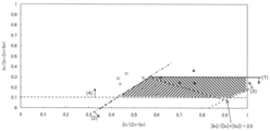
- FIG. 2 is a graph showing a region satisfying the range of the formula defined in the present invention.
- the hatched region in which the oblique line direction rises to the upper right (lower left region in FIG. 2) is the present invention when the In ratio is 0.5 or less.
- the range [the range satisfying the formulas (2) and (4)] is shown, and the hatched area with the diagonal direction falling to the lower right (the upper right area in FIG. 2) is the range of the present invention when the In ratio is more than 0.5 [formula
- FIG. 1 is a schematic cross-sectional view for explaining a thin film transistor including an oxide semiconductor.
- FIG. 2 is a graph showing a region satisfying the range of the formula defined in the present invention.
- the hatched region in which the oblique line direction rises to the upper right (lower left region in FIG. 2) is the present invention when the In ratio is 0.5 or less.
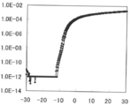
- 4A shows No. 1 of Example 1.
- FIG. FIG. 2 is a diagram showing the results of TFT characteristics for 2.
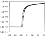
- 4B shows No. 1 of Example 1.
- FIG. 7 is a diagram showing the result of TFT characteristics for No. 7.
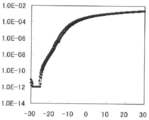
- FIG. 4C shows No. 1 of Example 1.
- FIG. 10 is a diagram showing the result of TFT characteristics for No. 10.
- FIG. 4D shows No. 1 of Example 1.
- 5A shows No. 1 of Example 1.
- 5B shows No. 1 of Example 1.
- FIG. 5C shows No. 1 of Example 1. It is a figure which shows the result of TFT characteristic about 13C.
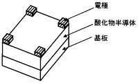
- 6 is a top view of a sample for evaluating the electron carrier concentration of an oxide semiconductor layer in Example 2.
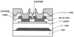
- FIG. FIG. 7 is a schematic cross-sectional view of a thin film transistor including an oxide semiconductor used in Example 2.
- IZTO In—Zn—Sn-based oxide
- active layer semiconductor layer
- TFT switching characteristics TFT characteristics
- Sputtering rate is high during sputtering
- Oxide has been studied to provide an oxide with no residue remaining during wet etching.
- Zn ratio represented by [Zn] / ([Zn] + [Sn]) described on the right side of the above (2) may be simply referred to as “Zn ratio” in order to distinguish it from the above. .
- a region that is, a region that satisfies the formulas (2) and (4)]
- a hatched region that exceeds the line is a region that satisfies the requirements of the present invention in the example (a) [that is, the formula ( Regions satisfying 1), (3), and (4)].
- ⁇ is a plot of the results of the present invention example that satisfies the requirements of the present invention for the example (a) above, and ⁇ is for the example (a) above.
- the result of the comparative example which does not satisfy the requirements of the present invention is plotted.
- ⁇ represents a plot of the results of the example of the present invention that satisfies the requirements of the present invention for the example of the above (a) among the examples described later
- ⁇ represents the above (a)
- the results of comparative examples that do not satisfy the requirements of the present invention are plotted for the examples. It can be seen that anything satisfying the requirements of the present invention is included in the range of the shaded portion.
- the above formula (3) is related to the prevention of residue generation during wet etching, and the above formulas (1) and (2) are both compatible with a high sputter rate and good TFT characteristics (switching characteristics). It is a related expression. Regarding the latter characteristic (coexistence of high sputter rate and good TFT characteristic), in the present invention, according to the In ratio represented by [In] / ([In] + [Sn]), When the In ratio is as low as 0.5 or less, the formula (2) is used as an index. When the In ratio is as large as more than 0.5 as in the above (a), the formula (1) is used as an index.
- the above formula (4) defines the lower limit of the In ratio ([In] / ([In] + [Zn] + [Sn])) in all metal elements, and ensures high mobility. Therefore, in both cases (a) and (b), the lower limit is set to 0.1 or more.
- the formula (3) is not defined. However, this does not require the formula (3) to be defined, but the formula (2) This is because the region satisfying the equation (4) includes the region of the equation (3) (see FIG. 2). Therefore, the region satisfying the equations (2) and (4) can not only achieve both a high sputter rate and good TFT characteristics, but also has a region that has an effect of preventing residue generation during wet etching [formula (3 It is also an area that satisfies
- Formula (1) is set from such a viewpoint, and in the example of (A) in which the In ratio exceeds 0.5, the above-described desired characteristics can be obtained with Formula (1) as a boundary. It can be seen that the example of the present invention ( ⁇ ) and the comparative example ( ⁇ ) where the above characteristics are not obtained can be well organized.
- the problem with IZTO film formation is that if In is large, the TFT becomes a conductor (no longer switches). Therefore, in order to switch the TFT, it is necessary to increase the oxygen partial pressure. However, if the oxygen partial pressure is increased, there is a problem that the sputtering rate decreases. In consideration of these problems, in order to increase the sputter rate (low oxygen partial pressure) while switching the TFT, the In ratio in all metal elements (specifically, [In] / ([In] + [Zn] + [Sn]) has been found necessary to be properly controlled.
- the In ratio in all metal elements is appropriately controlled according to the In ratio represented by [In] / ([In] + [Sn]). It turned out to be effective.
- SR1 In-Zn-Sn
- SR1 In-Zn-Sn
- an In—Ga—Zn oxide sputtering target (atomic ratio of In, Ga, Zn is 1: 1: 1) at the same oxygen partial pressure of 4%, an In—Ga—Zn oxide film (In , Ga, Zn atomic ratio is 1: 1: 1), when the sputtering rate (nm / min) is SR2 (In-Ga-Zn), the sputtering rate represented by SR1 / SR2.
- Ratio (SR) is 1.0 or more It means a thing.
- good TFT characteristics means that a voltage when the drain current is in the vicinity of 1 nA between the on-current and the off-current is defined as a threshold voltage, and Vth (absolute value) is measured when the threshold voltage of each TFT is measured. ) was evaluated as having excellent TFT characteristics.
- the above formula (3) is a formula related to prevention of residue generation during wet etching. As described above, it is desirable that no residue is generated during wet etching. However, the generation of the residue mainly involves Zn, and the residue is generated during wet etching due to an increase in the amount of Zn in the oxide film. For example, it is known that when an IZTO film is etched using oxalic acid that is widely used as a wet etchant, a hardly soluble zinc oxalate crystal is precipitated and a residue is generated. Therefore, the present inventors have studied various requirements for preventing generation of residues during wet etching, and as a result, set the above equation (3) in relation to the Zn ratio.
- the lower limit of the Zn ratio in all metal elements is not particularly limited from the viewpoint of wet etching properties, but patterning is performed as the etching rate is lower. In view of the fact that it takes a long time, it is preferably 0.40 or more, and more preferably 0.45 or more.
- the oxide is formed by sputtering using a sputtering target (hereinafter also referred to as “target”).
- a sputtering target hereinafter also referred to as “target”.
- an oxide can be formed by a chemical film formation method such as a coating method, a thin film excellent in in-plane uniformity of components and film thickness can be easily formed by a sputtering method.
- a target used in the sputtering method it is preferable to use a sputtering target containing the above-mentioned elements and having the same composition as the desired oxide, thereby forming a thin film having a desired component composition without fear of composition deviation. Can do.
- a film may be formed by using a co-sputtering method (Co-Sputter method) in which two targets having different compositions are discharged simultaneously, and targets such as In 2 O 3 , ZnO, SnO 2 or a mixture thereof are simultaneously used.
- a film having a desired composition can be obtained by discharging.
- the target can be manufactured by, for example, a powder sintering method.
- the substrate temperature at this time may be room temperature or a heated state.
- the threshold voltage shows a positive shift in the region where the oxygen partial pressure is high, but the sputtering rate is decreased. Therefore, it is necessary to make the composition exhibit good TFT characteristics even in a low sputtering partial pressure region where high sputtering rate and good etching characteristics can be ensured. From this viewpoint, the present invention satisfies the above requirements. Set.
- the oxygen partial pressure during sputtering is preferably controlled to approximately 18% or less, and preferably to 15% or less. More preferably, it is controlled.
- an inert gas such as Ar, Kr, or Xe can be used as the atmospheric gas during sputtering.
- the oxygen partial pressure in the present invention means the ratio of oxygen to all of these gases.
- the film thickness of the oxide film formed as described above is not less than 30 nm and not more than 200 nm. It was found that an oxide semiconductor layer having an oxide film thickness exceeding the above upper limit cannot obtain a desired electron carrier concentration and cannot secure good TFT characteristics (see Examples described later). On the other hand, if the lower limit of the film thickness is not reached, it becomes difficult to control the film thickness during film formation.
- the film thickness is preferably 35 nm or more and 80 nm or less.
- the present invention includes a semiconductor layer of a TFT including the above oxide and a TFT including the semiconductor layer.
- the TFT is not particularly limited as long as it has at least a gate electrode, a gate insulating film, the above-described oxide semiconductor layer, a source electrode, and a drain electrode on a substrate.
- the semiconductor layer of the thin film transistor according to the present invention has an electron carrier concentration of 10 15 to 10 18 cm ⁇ 3 .
- the electron carrier concentration of the semiconductor layer is one of the determinants of the switching characteristics of the TFT. Generally, if the electron carrier concentration is too high, the TFT becomes a conductor and does not switch. On the other hand, if the electron carrier concentration is too low, the insulating properties of the TFT are increased and the resistance is increased. Further, even if switching is performed, there is a problem in that the on-current decreases in a high-resistance film. As described above, the TFT characteristics vary greatly depending on the electron carrier concentration. However, in the present invention, the electron carrier concentration is controlled within an appropriate range of 10 15 to 10 18 cm ⁇ 3 , so that excellent TFT characteristics (described later) are obtained. In this example, it was confirmed that the threshold voltage Vth was evaluated.
- the semiconductor layer of the present invention having the above electron carrier concentration is obtained by heat-treating any of the above oxides at 250 to 350 ° C. for 15 to 120 minutes (details will be described later).
- FIG. 1 illustrates a bottom-gate TFT, but the present invention is not limited thereto, and a top-gate TFT including a gate insulating film and a gate electrode in this order on an oxide semiconductor layer may be used.
- a gate electrode 2 and a gate insulating film 3 are formed on a substrate 1, and an oxide semiconductor layer 4 is formed thereon.
- a source / drain electrode 5 is formed on the oxide semiconductor layer 4, a protective film (insulating film) 6 is formed thereon, and the transparent conductive film 8 is electrically connected to the source / drain electrode 5 through the contact hole 7. It is connected to the.
- the method for forming the gate electrode 2 and the gate insulating film 3 on the substrate 1 is not particularly limited, and a commonly used method can be employed. Further, the types of the gate electrode 2 and the gate insulating film 3 are not particularly limited, and those commonly used can be used.
- the gate electrode an Al or Cu metal having a low electrical resistivity or an alloy thereof can be preferably used.
- the gate insulating film typically include a silicon oxide film, a silicon nitride film, and a silicon oxynitride film.
- a metal oxide such as TiO 2 , Al 2 O 3 , Y 2 O 3 , or a laminate of these can be used.
- the oxide semiconductor layer 4 is formed.
- the oxide semiconductor layer 4 is preferably formed by a DC sputtering method or an RF sputtering method using a sputtering target having the same composition as the thin film.
- the film may be formed by co-sputtering.
- the oxide semiconductor layer 4 is subjected to wet etching and then patterned.
- heat treatment pre-annealing
- a temperature of about 250 to 350 ° C. and a time of about 15 to 120 minutes As a result, the on-state current and the field effect mobility of the transistor characteristics are increased, and the transistor performance is improved.
- Preferred pre-annealing conditions are temperature: about 300 to 350 ° C., time: about 60 to 120 minutes.
- the source / drain electrodes 5 are formed.
- the type of the source / drain electrode is not particularly limited, and those commonly used can be used.
- a metal or alloy such as Al or Cu may be used like the gate electrode, or pure Ti may be used as in the examples described later.
- a laminated structure of metal can be used.
- a metal thin film can be formed by a magnetron sputtering method and then formed by a lift-off method.
- a protective film (insulating film) 6 is formed over the oxide semiconductor layer 4 by a CVD (Chemical Vapor Deposition) method.
- the surface of the oxide semiconductor film easily becomes conductive due to plasma damage caused by CVD (probably because oxygen vacancies generated on the surface of the oxide semiconductor serve as electron donors), thus avoiding the above problem. Therefore, in the embodiment described below, it was N 2 O plasma irradiation before the formation of the protective film.
- the conditions described in the following document were adopted as the irradiation conditions of N 2 O plasma. J. et al. Park et al., Appl. Phys. Lett. , 1993, 053505 (2008).
- the transparent conductive film 8 is electrically connected to the drain electrode 5 through the contact hole 7.
- the types of the transparent conductive film and the drain electrode are not particularly limited, and commonly used ones can be used.
- As the drain electrode for example, those exemplified for the source / drain electrodes described above can be used.
- Example 1 Based on the method described above, the thin film transistor (TFT) shown in FIG. 1 was fabricated and various characteristics were evaluated.
- TFT thin film transistor
- a 100 nm Mo thin film was formed as a gate electrode on a glass substrate (Corning Eagle 2000, diameter 100 mm ⁇ thickness 0.7 mm), and then patterned by photolithography and wet etching. A film SiO 2 (250 nm) was formed.
- As the gate electrode a pure Mo sputtering target was used, and a film was formed by DC sputtering at a film forming temperature: room temperature, a film forming power: 300 W, a carrier gas: Ar, and a gas pressure: 2 mTorr.
- the gate insulating film was formed by plasma CVD using a carrier gas: a mixed gas of SiH 4 and N 2 , film formation power: 100 W, and film formation temperature: 300 ° C.
- IZTO thin films having various compositions shown in Tables 1 and 2 are subjected to IZTO sputtering having a composition corresponding to the above table.
- Table 2 using the target, the oxygen partial pressure was changed and the film was formed by the sputtering method.
- no. 5A and No. 5B is the same as [In] and [Zn] and [Sn] are substantially the same.
- the oxygen partial pressure ratio was 4%.
- the film was formed with an oxygen partial pressure ratio of 10%, characteristics such as a sputtering rate ratio and Vth are different even with the same composition.
- the apparatus used for sputtering was “CS-200” manufactured by ULVAC, Inc., and the sputtering conditions were as follows.
- Substrate temperature room temperature
- Gas pressure 1 mTorr
- Film thickness 40nm
- Use target size ⁇ 4 inch x 5mm
- the sputtering rate (nm / min) of the IGZO thin film was calculated.
- an In—Ga—Zn sputtering target composed of In, Ga, and Zn [wherein, the content (atomic%) of In, Ga, and Zn in the sputtering target has a relationship of 1: 1: 1. Satisfied.
- the IGZO thin film was formed under the same sputtering conditions as the IZTO thin film except that the oxygen partial pressure was 4% (constant), and the film thickness of the obtained IGZO thin film was divided by the film formation time. Calculated.
- the contents (atomic%) of In, Ga, and Zn in the IGZO thin film thus obtained also satisfy the 1: 1: 1 relationship. This is referred to as SR2 (In-Ga-Zn).
- each content of the metal element was analyzed by XPS (X-ray Photoelectron Spectroscopy) method.
- a pre-annealing process was performed in a water vapor atmosphere at 350 ° C. for 1 hour in the air.
- pure Mo was used to form source / drain electrodes by a lift-off method. Specifically, after patterning using a photoresist, a Mo thin film was formed by DC sputtering (film thickness was 100 nm). The method for forming the Mo thin film for the source / drain electrodes is the same as that for the gate electrode described above. Next, it was immersed in acetone, and unnecessary photoresist was removed by applying an ultrasonic cleaner, so that the channel length of the TFT was 10 ⁇ m and the channel width was 200 ⁇ m.
- a protective film for protecting the oxide semiconductor layer was formed.
- a laminated film (total film thickness 364 nm) of SiO 2 (film thickness 114 nm) and SiN (film thickness 250 nm) was used.
- the above-mentioned SiO 2 and SiN were formed using “PD-220NL” manufactured by Samco and using the plasma CVD method.
- SiO 2 and SiN films were sequentially formed.
- a mixed gas of N 2 O and SiH 4 was used for forming the SiO 2 film, and a mixed gas of SiH 4 , N 2 , and NH 3 was used for forming the SiN film.
- the film formation power was 100 W and the film formation temperature was 150 ° C.
- ITO film film thickness: 80 nm
- a carrier gas a mixed gas of argon and oxygen gas
- film formation power 200 W
- gas pressure 5 mTorr
- transistor characteristics drain current-gate voltage characteristics, Id-Vg characteristics
- Id-Vg characteristics semiconductor parameter analyzer “4156C” manufactured by Agilent Technologies. Detailed measurement conditions are as follows. Source voltage: 0V Drain voltage: 10V Gate voltage: -30 to 30V (measurement interval: 0.25V)
- Threshold voltage The threshold voltage is roughly a value of a gate voltage when the transistor shifts from an off state (a state where the drain current is low) to an on state (a state where the drain current is high).
- the voltage when the drain current is around 1 nA between the on-current and the off-current is defined as the threshold voltage, and the threshold voltage of each TFT is measured.
- a sample having a Vth (absolute value) of 17.5 V or less was accepted.
- the results of drain current-gate voltage characteristics are shown in FIG. 4A (No. 2), FIG. 4B (No. 7), and FIG. ), As shown in FIG. 4D (No. 5B). Further, No. 2 in Table 2 does not satisfy the requirements of the present invention.
- the results of drain current-gate voltage characteristics (Id-Vg characteristics) for 13A to 13C are shown in FIG. 5A (No. 13A), FIG. 5B (No. 13B), and FIG. 5C (No. 13C). In these figures, the vertical axis is Id (A), and the horizontal axis is Vg (V). Since the measurement was performed twice, both results are shown in these figures.
- those satisfying the requirements of the present invention are such that, as shown in FIGS. 4A to 4D, the drain current Id becomes 8 as the gate voltage Vg changes from ⁇ 30V to 30V before the formation of the protective film. It has increased by an order of magnitude, and good switching characteristics were obtained.
- carrier mobility field effect mobility
- carrier mobility field effect mobility
- C ox Capacitance of insulating film W: Channel width L: Channel length V th : Threshold voltage
- Table 2 shows each No. Is provided with a “remarks column” and satisfying [In] / ([In] + [Sn]) ⁇ 0.5, (A), [In] / ([In] + [Sn])> 0. Items that satisfy 5 were marked with (A).
- those satisfying the formulas (2) and (4) are examples of the present invention
- those satisfying the formulas (1), (3) and (4) are satisfied.
- all examples satisfy the relationship of Expression (4).
- “ ⁇ ” is marked in the column of “Relationship of Formula (2)” to satisfy the relationship of Formula (2), and “ ⁇ ” is not satisfied to satisfy the relationship of Formula (2).
- “determination 1” and “determination 2” fields are provided for each characteristic, and “ ⁇ ” is given to those that satisfy the acceptance criteria of this example, and “x” is assigned to those that do not satisfy the acceptance criteria of this example. .
- Vth absolute value
- SR sputtering rate ratio
- 1, 4, 6A, 6B, 8A, 8B, 9A, and 9B have high sputter rate ratios to satisfy the relationship of Equation (3), and no residue was generated during wet etching. Since the relationship was not satisfied, the absolute value of the threshold voltage increased and the TFT characteristics deteriorated.
- 13A to 13C have high sputter rate ratios to satisfy the relationship of the equation (3) and no residue was generated during wet etching, but the absolute value of the threshold voltage was not to satisfy the relationship of the equation (1).
- the TFT characteristics increased and the TFT characteristics deteriorated.
- the sputtering rate decreases as the oxygen partial pressure during sputtering increases. That is, as described above, No. in the table. 5A and No. 5B; 6A and No. 6B; 8A and No. 8B; 9A and No. 9B; 13A and No. 13B and No. 13C is an example in which the composition of IZTO is substantially the same, and the film is formed by changing the oxygen partial pressure ratio during sputtering. However, as the oxygen partial pressure ratio increases (A ⁇ B ⁇ C), the composition of IZTO increases. Regardless, the sputter rate ratio tended to decrease.
- FIG. 3 is a graph showing the influence of the oxygen partial pressure during sputtering on the sputtering rate. Specifically, FIG. Sputtering rate ratios were examined in the same manner as described above except that the compositions of 1, 4 and 9 were used and the oxygen partial pressure was variously changed within the range of 3 to 50% as shown in Table 3. The result is shown. For reference, Table 3 also shows the results of the sputtering rate. In FIG. 3, the oxygen partial pressure is shown as a flow rate ratio, not as a percentage.
- the oxygen partial pressure during film formation is preferably reduced to about 18% or less in order to ensure a desired high sputtering rate.
- the No. in Table 2 that satisfies all the requirements specified in the present invention If an In—Zn—Sn-based oxide semiconductor having a composition of 2, 3, 5, 7, 10 to 12 is used, the threshold voltage is high, the etching characteristics during wet etching, the sputtering rate during sputtering are excellent, and the conventional It was confirmed that it has a high mobility that is at least twice that of IGZO (mobility 7) and has good TFT characteristics. Therefore, according to the present invention, it is possible to provide an oxide semiconductor having high TFT characteristics, excellent manufacturing efficiency, excellent patterning property during wet etching, and a good yield.
- IGZO mobility 7
- Example (A) above with In ratio> 0.5 is a simulation of IZTO having the composition described in Patent Document 2 described above, and was conducted by changing the oxygen partial pressure. is there.
- FIGS. 5A to 5C it can be seen that the TFT characteristics cannot be improved unless the oxygen partial pressure is increased as shown in FIGS. 5A to 5C.
- Example 2 In this example, various samples (A1 to A7 in Table 4) were manufactured by changing the sputtering time when an oxide film was formed by a sputtering method and the pre-annealing conditions after the oxide film was formed. The relationship between the electron carrier concentration of the layer and the TFT characteristics (threshold voltage Vth) was examined.
- No. 1 in Table 1 above. 7 was prepared using the IZTO thin film No. 7 (which satisfies the composition of the present invention), and the electron carrier concentration was measured.
- the TFT shown in FIG. 1 was manufactured under the same film thickness and the same heat treatment conditions as the sample, and the threshold voltage Vth was measured in the same manner as in Example 1.
- a pre-annealing process was performed in the air and in a steam atmosphere.
- the heat treatment temperature and time of each sample at this time are as follows. For comparison, pre-annealing treatment was not performed in A3 below.
- Pre-annealing conditions No. A1 (film thickness 500 nm, temperature: 350 ° C., time: 30 minutes)
- No. A2 film thickness 40 nm, temperature: 350 ° C., time: 30 minutes
- No. A4 film thickness 40 nm, temperature: 350 ° C., time: 120 minutes) No.
- A5 film thickness 40 nm, temperature: 400 ° C., time: 30 minutes
- A6 film thickness 40 nm, temperature: 400 ° C., time: 120 minutes
- No. A7 film thickness 40 nm, temperature: 380 ° C., time: 30 minutes
- an electrode was formed by sputtering using pure Au.
- the apparatus used for sputtering was “CS-200” manufactured by ULVAC, Inc., and the electrodes were patterned by mask sputtering. After forming the pure Au electrode in this manner, the sample was divided to obtain Hall effect measurement samples (evaluation samples for evaluating the electron carrier concentration of the oxide semiconductor layer) shown in FIG.
- the Hall effect measurement (van der Pauw method) was performed at room temperature using each Hall effect measurement sample thus obtained, and the electron carrier concentration was evaluated.
- the TFT shown in FIG. 7 was fabricated with the same film thickness and the same heat treatment conditions as the Hall effect measurement sample of FIG.
- the threshold voltage Vth was evaluated in the same manner as in 1.
- the TFT shown in FIG. 7 is different from the TFT of FIG. 1 used in Example 1 described above only in that a surface protective film is formed on the oxide semiconductor layer in FIG. 1 has no surface protective film on the oxide semiconductor layer 4). Since the oxide semiconductor layer is easily damaged by heat treatment during film formation and the TFT characteristics are deteriorated, a surface protective film such as SiO 2 is usually formed to protect the surface of the oxide semiconductor layer. It is done.
- a Mo thin film of 100 nm and a gate insulating film SiO 2 (250 nm) were formed as gate electrodes. Films were sequentially formed.
- a surface protective film SiO 2 , film thickness 100 nm
- the SiO 2 film was formed using “PD-220NL” manufactured by Samco and using the plasma CVD method. In this example, a mixed gas of N 2 O and SiH 4 was used, the deposition power was 100 W, and the deposition temperature was 200 ° C.
- the surface protective film thus formed was subjected to patterning for electrode formation by photolithography and dry etching in order to make contact between the semiconductor layer and the source / drain electrodes.
- the TFT has a channel length of 10 ⁇ m, a channel width of 25 ⁇ m, and a protective film for protecting the oxide semiconductor layer [ A laminated film of SiO 2 (film thickness 114 nm) and SiN (film thickness 250 nm) (total film thickness 364 nm)] was formed. Thereafter, in the same manner as in Example 1 described above, a contact hole for probing for transistor characteristic evaluation and an ITO film were formed on the protective film, and the TFT of FIG. 7 was produced.
- the threshold voltage Vth was evaluated in the same manner as in Example 1.
- Table 4 shows these results together.
- ⁇ is given to those satisfying the electron carrier concentration range (10 15 to 10 18 cm ⁇ 3 ) of the oxide semiconductor layer according to the present invention, and “ “ ⁇ ” was added.
- the threshold voltage Vth varies depending on the electron carrier concentration, but the electron carrier concentration satisfies the requirements of the present invention.
Landscapes
- Physics & Mathematics (AREA)
- Nonlinear Science (AREA)
- Optics & Photonics (AREA)
- Engineering & Computer Science (AREA)
- Microelectronics & Electronic Packaging (AREA)
- Mathematical Physics (AREA)
- Chemical & Material Sciences (AREA)
- Crystallography & Structural Chemistry (AREA)
- General Physics & Mathematics (AREA)
- Thin Film Transistor (AREA)
- Physical Vapour Deposition (AREA)
- Physical Deposition Of Substances That Are Components Of Semiconductor Devices (AREA)
Abstract
Priority Applications (4)
| Application Number | Priority Date | Filing Date | Title |
|---|---|---|---|
| US14/004,020 US20130341617A1 (en) | 2011-03-09 | 2012-03-08 | Oxide for semiconductor layer of thin-film transistor, semiconductor layer of thin-film transistor having said oxide, and thin-film transistor |
| CN201280012067.6A CN103415926B (zh) | 2011-03-09 | 2012-03-08 | 薄膜晶体管的半导体层用氧化物,具备上述氧化物的薄膜晶体管的半导体层和薄膜晶体管 |
| KR1020137025547A KR101509115B1 (ko) | 2011-03-09 | 2012-03-08 | 박막 트랜지스터의 반도체층용 산화물, 상기 산화물을 구비한 박막 트랜지스터의 반도체층 및 박막 트랜지스터 |
| US15/290,715 US10256091B2 (en) | 2011-03-09 | 2016-10-11 | Oxide for semiconductor layer of thin-film transistor, semiconductor layer of thin-film transistor having said oxide, and thin-film transistor |
Applications Claiming Priority (4)
| Application Number | Priority Date | Filing Date | Title |
|---|---|---|---|
| JP2011-052179 | 2011-03-09 | ||
| JP2011052179 | 2011-03-09 | ||
| JP2011289740 | 2011-12-28 | ||
| JP2011-289740 | 2011-12-28 |
Related Child Applications (2)
| Application Number | Title | Priority Date | Filing Date |
|---|---|---|---|
| US14/004,020 A-371-Of-International US20130341617A1 (en) | 2011-03-09 | 2012-03-08 | Oxide for semiconductor layer of thin-film transistor, semiconductor layer of thin-film transistor having said oxide, and thin-film transistor |
| US15/290,715 Continuation US10256091B2 (en) | 2011-03-09 | 2016-10-11 | Oxide for semiconductor layer of thin-film transistor, semiconductor layer of thin-film transistor having said oxide, and thin-film transistor |
Publications (1)
| Publication Number | Publication Date |
|---|---|
| WO2012121332A1 true WO2012121332A1 (fr) | 2012-09-13 |
Family
ID=46798287
Family Applications (1)
| Application Number | Title | Priority Date | Filing Date |
|---|---|---|---|
| PCT/JP2012/055966 Ceased WO2012121332A1 (fr) | 2011-03-09 | 2012-03-08 | Oxyde pour couche semi-conductrice pour transistor à couche mince, couche semi-conductrice pour transistor à couche mince comprenant ledit oxyde et transistor à couche mince |
Country Status (6)
| Country | Link |
|---|---|
| US (2) | US20130341617A1 (fr) |
| JP (2) | JP2013153118A (fr) |
| KR (1) | KR101509115B1 (fr) |
| CN (1) | CN103415926B (fr) |
| TW (1) | TWI580055B (fr) |
| WO (1) | WO2012121332A1 (fr) |
Cited By (2)
| Publication number | Priority date | Publication date | Assignee | Title |
|---|---|---|---|---|
| JPWO2015122250A1 (ja) * | 2014-02-17 | 2017-03-30 | 三菱瓦斯化学株式会社 | インジウムと亜鉛とスズおよび酸素からなる酸化物のエッチング用液体組成物およびエッチング方法 |
| WO2017094547A1 (fr) * | 2015-11-30 | 2017-06-08 | 国立大学法人東京工業大学 | Procédé de fabrication d'élément de conversion photoélectrique |
Families Citing this family (12)
| Publication number | Priority date | Publication date | Assignee | Title |
|---|---|---|---|---|
| WO2013168748A1 (fr) | 2012-05-09 | 2013-11-14 | 株式会社神戸製鋼所 | Transistor à film mince et dispositif d'affichage |
| JP6068232B2 (ja) | 2012-05-30 | 2017-01-25 | 株式会社神戸製鋼所 | 薄膜トランジスタの半導体層用酸化物、薄膜トランジスタ、表示装置およびスパッタリングターゲット |
| JP6002088B2 (ja) | 2012-06-06 | 2016-10-05 | 株式会社神戸製鋼所 | 薄膜トランジスタ |
| CN104335353B (zh) | 2012-06-06 | 2017-04-05 | 株式会社神户制钢所 | 薄膜晶体管 |
| JP2014225626A (ja) | 2012-08-31 | 2014-12-04 | 株式会社神戸製鋼所 | 薄膜トランジスタおよび表示装置 |
| JP6134230B2 (ja) | 2012-08-31 | 2017-05-24 | 株式会社神戸製鋼所 | 薄膜トランジスタおよび表示装置 |
| US9153649B2 (en) * | 2012-11-30 | 2015-10-06 | Semiconductor Energy Laboratory Co., Ltd. | Semiconductor device and method for evaluating semiconductor device |
| TWI669761B (zh) * | 2014-05-30 | 2019-08-21 | 日商半導體能源研究所股份有限公司 | 半導體裝置、包括該半導體裝置的顯示裝置 |
| TWI666776B (zh) | 2014-06-20 | 2019-07-21 | 日商半導體能源研究所股份有限公司 | 半導體裝置以及包括該半導體裝置的顯示裝置 |
| CN104966698B (zh) * | 2015-07-16 | 2018-07-17 | 深圳市华星光电技术有限公司 | 阵列基板、阵列基板的制造方法及显示装置 |
| JP6903503B2 (ja) * | 2017-07-05 | 2021-07-14 | 三菱電機株式会社 | 薄膜トランジスタ基板、液晶表示装置および薄膜トランジスタ基板の製造方法 |
| US12009432B2 (en) | 2021-03-05 | 2024-06-11 | Semiconductor Energy Laboratory Co., Ltd. | Transistor and display device |
Citations (5)
| Publication number | Priority date | Publication date | Assignee | Title |
|---|---|---|---|---|
| WO2008117739A1 (fr) * | 2007-03-23 | 2008-10-02 | Idemitsu Kosan Co., Ltd. | Dispositif semi-conducteur, film mince semi-conducteur polycristallin, procédé de fabrication d'un film mince semi-conducteur polycristallin, transistor à effet de champ, et procédé de fabrication d'un transistor à effet de champ. |
| JP2008243928A (ja) * | 2007-03-26 | 2008-10-09 | Idemitsu Kosan Co Ltd | 非晶質酸化物半導体薄膜、その製造方法、薄膜トランジスタの製造方法、電界効果型トランジスタ、発光装置、表示装置及びスパッタリングターゲット |
| JP2009253204A (ja) * | 2008-04-10 | 2009-10-29 | Idemitsu Kosan Co Ltd | 酸化物半導体を用いた電界効果型トランジスタ及びその製造方法 |
| WO2010023889A1 (fr) * | 2008-08-27 | 2010-03-04 | 出光興産株式会社 | Transistor à effet de champ, son procédé de fabrication et cible de pulvérisation cathodique |
| WO2010067571A1 (fr) * | 2008-12-12 | 2010-06-17 | 出光興産株式会社 | Corps fritté en oxyde composite et cible de pulvérisation associée |
Family Cites Families (10)
| Publication number | Priority date | Publication date | Assignee | Title |
|---|---|---|---|---|
| US6351068B2 (en) * | 1995-12-20 | 2002-02-26 | Mitsui Chemicals, Inc. | Transparent conductive laminate and electroluminescence light-emitting element using same |
| JP4709816B2 (ja) | 1999-03-16 | 2011-06-29 | エルジー ディスプレイ カンパニー リミテッド | 薄膜トランジスタ基板の製造方法 |
| WO2001038599A1 (fr) * | 1999-11-25 | 2001-05-31 | Idemitsu Kosan Co., Ltd. | Cible de pulverisation cathodique, oxyde electro-conducteur transparent, et procede d'elaboration d'une cible de pulverisation cathodique |
| US20050017244A1 (en) * | 2003-07-25 | 2005-01-27 | Randy Hoffman | Semiconductor device |
| EP3360855B1 (fr) * | 2006-05-18 | 2020-03-18 | Hydro-Quebec | Procédé de préparation de céramiques, céramiques ainsi obtenues et leurs utilisations notamment comme cible pour pulvérisation cathodique |
| EP2471972B1 (fr) * | 2006-12-13 | 2014-01-29 | Idemitsu Kosan Co., Ltd. | Cible de pulvérisation |
| JP5320746B2 (ja) * | 2007-03-28 | 2013-10-23 | 凸版印刷株式会社 | 薄膜トランジスタ |
| JPWO2009028453A1 (ja) | 2007-08-31 | 2010-12-02 | コニカミノルタホールディングス株式会社 | 薄膜トランジスタ |
| JP5213458B2 (ja) | 2008-01-08 | 2013-06-19 | キヤノン株式会社 | アモルファス酸化物及び電界効果型トランジスタ |
| JP2012094853A (ja) * | 2010-09-30 | 2012-05-17 | Kobe Steel Ltd | 配線構造 |
-
2012
- 2012-03-07 JP JP2012050855A patent/JP2013153118A/ja active Pending
- 2012-03-08 US US14/004,020 patent/US20130341617A1/en not_active Abandoned
- 2012-03-08 CN CN201280012067.6A patent/CN103415926B/zh active Active
- 2012-03-08 WO PCT/JP2012/055966 patent/WO2012121332A1/fr not_active Ceased
- 2012-03-08 KR KR1020137025547A patent/KR101509115B1/ko active Active
- 2012-03-09 TW TW101108128A patent/TWI580055B/zh active
-
2016
- 2016-09-30 JP JP2016194848A patent/JP6294428B2/ja active Active
- 2016-10-11 US US15/290,715 patent/US10256091B2/en active Active
Patent Citations (5)
| Publication number | Priority date | Publication date | Assignee | Title |
|---|---|---|---|---|
| WO2008117739A1 (fr) * | 2007-03-23 | 2008-10-02 | Idemitsu Kosan Co., Ltd. | Dispositif semi-conducteur, film mince semi-conducteur polycristallin, procédé de fabrication d'un film mince semi-conducteur polycristallin, transistor à effet de champ, et procédé de fabrication d'un transistor à effet de champ. |
| JP2008243928A (ja) * | 2007-03-26 | 2008-10-09 | Idemitsu Kosan Co Ltd | 非晶質酸化物半導体薄膜、その製造方法、薄膜トランジスタの製造方法、電界効果型トランジスタ、発光装置、表示装置及びスパッタリングターゲット |
| JP2009253204A (ja) * | 2008-04-10 | 2009-10-29 | Idemitsu Kosan Co Ltd | 酸化物半導体を用いた電界効果型トランジスタ及びその製造方法 |
| WO2010023889A1 (fr) * | 2008-08-27 | 2010-03-04 | 出光興産株式会社 | Transistor à effet de champ, son procédé de fabrication et cible de pulvérisation cathodique |
| WO2010067571A1 (fr) * | 2008-12-12 | 2010-06-17 | 出光興産株式会社 | Corps fritté en oxyde composite et cible de pulvérisation associée |
Cited By (3)
| Publication number | Priority date | Publication date | Assignee | Title |
|---|---|---|---|---|
| JPWO2015122250A1 (ja) * | 2014-02-17 | 2017-03-30 | 三菱瓦斯化学株式会社 | インジウムと亜鉛とスズおよび酸素からなる酸化物のエッチング用液体組成物およびエッチング方法 |
| WO2017094547A1 (fr) * | 2015-11-30 | 2017-06-08 | 国立大学法人東京工業大学 | Procédé de fabrication d'élément de conversion photoélectrique |
| JPWO2017094547A1 (ja) * | 2015-11-30 | 2018-09-13 | 国立大学法人東京工業大学 | 光電変換素子を製造する方法 |
Also Published As
| Publication number | Publication date |
|---|---|
| JP2013153118A (ja) | 2013-08-08 |
| US20170053800A1 (en) | 2017-02-23 |
| CN103415926B (zh) | 2016-06-29 |
| US20130341617A1 (en) | 2013-12-26 |
| JP6294428B2 (ja) | 2018-03-14 |
| US10256091B2 (en) | 2019-04-09 |
| CN103415926A (zh) | 2013-11-27 |
| TW201301522A (zh) | 2013-01-01 |
| KR101509115B1 (ko) | 2015-04-07 |
| JP2017050545A (ja) | 2017-03-09 |
| KR20140033348A (ko) | 2014-03-18 |
| TWI580055B (zh) | 2017-04-21 |
Similar Documents
| Publication | Publication Date | Title |
|---|---|---|
| JP6294428B2 (ja) | 薄膜トランジスタの半導体層用酸化物の製造方法、および薄膜トランジスタの特性を向上する方法 | |
| JP6018551B2 (ja) | 薄膜トランジスタ | |
| JP5977569B2 (ja) | 薄膜トランジスタ構造、ならびにその構造を備えた薄膜トランジスタおよび表示装置 | |
| JP6043244B2 (ja) | 薄膜トランジスタ | |
| JP5718072B2 (ja) | 薄膜トランジスタの半導体層用酸化物およびスパッタリングターゲット、並びに薄膜トランジスタ | |
| JP2013070010A (ja) | 薄膜トランジスタの半導体層用酸化物およびスパッタリングターゲット、並びに薄膜トランジスタ | |
| JP2012151469A (ja) | 薄膜トランジスタの半導体層用酸化物およびスパッタリングターゲット、並びに薄膜トランジスタ | |
| KR102124867B1 (ko) | 박막 트랜지스터의 반도체층용 산화물 및 스퍼터링 타깃 및 박막 트랜지스터 | |
| JP6068232B2 (ja) | 薄膜トランジスタの半導体層用酸化物、薄膜トランジスタ、表示装置およびスパッタリングターゲット | |
| JP2012124446A (ja) | 薄膜トランジスタの半導体層用酸化物およびスパッタリングターゲット、並びに薄膜トランジスタ | |
| JP2012033854A (ja) | 薄膜トランジスタの半導体層用酸化物およびスパッタリングターゲット、並びに薄膜トランジスタ | |
| JP5722293B2 (ja) | 薄膜トランジスタ | |
| JP5645737B2 (ja) | 薄膜トランジスタ構造および表示装置 | |
| JP2013207100A (ja) | 薄膜トランジスタ | |
| JP2016026389A (ja) | 薄膜トランジスタの半導体層用酸化物およびスパッタリングターゲット、並びに薄膜トランジスタ | |
| WO2016035503A1 (fr) | Transistor a couches minces |
Legal Events
| Date | Code | Title | Description |
|---|---|---|---|
| 121 | Ep: the epo has been informed by wipo that ep was designated in this application |
Ref document number: 12755548 Country of ref document: EP Kind code of ref document: A1 |
|
| NENP | Non-entry into the national phase |
Ref country code: DE |
|
| WWE | Wipo information: entry into national phase |
Ref document number: 14004020 Country of ref document: US |
|
| ENP | Entry into the national phase |
Ref document number: 20137025547 Country of ref document: KR Kind code of ref document: A |
|
| 122 | Ep: pct application non-entry in european phase |
Ref document number: 12755548 Country of ref document: EP Kind code of ref document: A1 |