WO2012132385A1 - 光電場増強デバイスの製造方法 - Google Patents
光電場増強デバイスの製造方法 Download PDFInfo
- Publication number
- WO2012132385A1 WO2012132385A1 PCT/JP2012/002072 JP2012002072W WO2012132385A1 WO 2012132385 A1 WO2012132385 A1 WO 2012132385A1 JP 2012002072 W JP2012002072 W JP 2012002072W WO 2012132385 A1 WO2012132385 A1 WO 2012132385A1
- Authority
- WO
- WIPO (PCT)
- Prior art keywords
- metal
- convex structure
- layer
- photoelectric field
- field enhancement
- Prior art date
- Legal status (The legal status is an assumption and is not a legal conclusion. Google has not performed a legal analysis and makes no representation as to the accuracy of the status listed.)
- Ceased
Links
Images






Classifications
-
- G—PHYSICS
- G01—MEASURING; TESTING
- G01N—INVESTIGATING OR ANALYSING MATERIALS BY DETERMINING THEIR CHEMICAL OR PHYSICAL PROPERTIES
- G01N21/00—Investigating or analysing materials by the use of optical means, i.e. using sub-millimetre waves, infrared, visible or ultraviolet light
- G01N21/62—Systems in which the material investigated is excited whereby it emits light or causes a change in wavelength of the incident light
- G01N21/63—Systems in which the material investigated is excited whereby it emits light or causes a change in wavelength of the incident light optically excited
- G01N21/65—Raman scattering
- G01N21/658—Raman scattering enhancement Raman, e.g. surface plasmons
-
- G—PHYSICS
- G01—MEASURING; TESTING
- G01J—MEASUREMENT OF INTENSITY, VELOCITY, SPECTRAL CONTENT, POLARISATION, PHASE OR PULSE CHARACTERISTICS OF INFRARED, VISIBLE OR ULTRAVIOLET LIGHT; COLORIMETRY; RADIATION PYROMETRY
- G01J3/00—Spectrometry; Spectrophotometry; Monochromators; Measuring colours
- G01J3/28—Investigating the spectrum
- G01J3/44—Raman spectrometry; Scattering spectrometry ; Fluorescence spectrometry
-
- C—CHEMISTRY; METALLURGY
- C03—GLASS; MINERAL OR SLAG WOOL
- C03C—CHEMICAL COMPOSITION OF GLASSES, GLAZES OR VITREOUS ENAMELS; SURFACE TREATMENT OF GLASS; SURFACE TREATMENT OF FIBRES OR FILAMENTS MADE FROM GLASS, MINERALS OR SLAGS; JOINING GLASS TO GLASS OR OTHER MATERIALS
- C03C17/00—Surface treatment of glass, not in the form of fibres or filaments, by coating
- C03C17/06—Surface treatment of glass, not in the form of fibres or filaments, by coating with metals
- C03C17/09—Surface treatment of glass, not in the form of fibres or filaments, by coating with metals by deposition from the vapour phase
-
- C—CHEMISTRY; METALLURGY
- C23—COATING METALLIC MATERIAL; COATING MATERIAL WITH METALLIC MATERIAL; CHEMICAL SURFACE TREATMENT; DIFFUSION TREATMENT OF METALLIC MATERIAL; COATING BY VACUUM EVAPORATION, BY SPUTTERING, BY ION IMPLANTATION OR BY CHEMICAL VAPOUR DEPOSITION, IN GENERAL; INHIBITING CORROSION OF METALLIC MATERIAL OR INCRUSTATION IN GENERAL
- C23C—COATING METALLIC MATERIAL; COATING MATERIAL WITH METALLIC MATERIAL; SURFACE TREATMENT OF METALLIC MATERIAL BY DIFFUSION INTO THE SURFACE, BY CHEMICAL CONVERSION OR SUBSTITUTION; COATING BY VACUUM EVAPORATION, BY SPUTTERING, BY ION IMPLANTATION OR BY CHEMICAL VAPOUR DEPOSITION, IN GENERAL
- C23C14/00—Coating by vacuum evaporation, by sputtering or by ion implantation of the coating forming material
- C23C14/06—Coating by vacuum evaporation, by sputtering or by ion implantation of the coating forming material characterised by the coating material
- C23C14/14—Metallic material, boron or silicon
- C23C14/18—Metallic material, boron or silicon on other inorganic substrates
-
- C—CHEMISTRY; METALLURGY
- C23—COATING METALLIC MATERIAL; COATING MATERIAL WITH METALLIC MATERIAL; CHEMICAL SURFACE TREATMENT; DIFFUSION TREATMENT OF METALLIC MATERIAL; COATING BY VACUUM EVAPORATION, BY SPUTTERING, BY ION IMPLANTATION OR BY CHEMICAL VAPOUR DEPOSITION, IN GENERAL; INHIBITING CORROSION OF METALLIC MATERIAL OR INCRUSTATION IN GENERAL
- C23C—COATING METALLIC MATERIAL; COATING MATERIAL WITH METALLIC MATERIAL; SURFACE TREATMENT OF METALLIC MATERIAL BY DIFFUSION INTO THE SURFACE, BY CHEMICAL CONVERSION OR SUBSTITUTION; COATING BY VACUUM EVAPORATION, BY SPUTTERING, BY ION IMPLANTATION OR BY CHEMICAL VAPOUR DEPOSITION, IN GENERAL
- C23C14/00—Coating by vacuum evaporation, by sputtering or by ion implantation of the coating forming material
- C23C14/58—After-treatment
- C23C14/5846—Reactive treatment
- C23C14/5853—Oxidation
-
- C—CHEMISTRY; METALLURGY
- C23—COATING METALLIC MATERIAL; COATING MATERIAL WITH METALLIC MATERIAL; CHEMICAL SURFACE TREATMENT; DIFFUSION TREATMENT OF METALLIC MATERIAL; COATING BY VACUUM EVAPORATION, BY SPUTTERING, BY ION IMPLANTATION OR BY CHEMICAL VAPOUR DEPOSITION, IN GENERAL; INHIBITING CORROSION OF METALLIC MATERIAL OR INCRUSTATION IN GENERAL
- C23C—COATING METALLIC MATERIAL; COATING MATERIAL WITH METALLIC MATERIAL; SURFACE TREATMENT OF METALLIC MATERIAL BY DIFFUSION INTO THE SURFACE, BY CHEMICAL CONVERSION OR SUBSTITUTION; COATING BY VACUUM EVAPORATION, BY SPUTTERING, BY ION IMPLANTATION OR BY CHEMICAL VAPOUR DEPOSITION, IN GENERAL
- C23C28/00—Coating for obtaining at least two superposed coatings either by methods not provided for in a single one of groups C23C2/00 - C23C26/00 or by combinations of methods provided for in subclasses C23C and C25C or C25D
- C23C28/30—Coatings combining at least one metallic layer and at least one inorganic non-metallic layer
- C23C28/32—Coatings combining at least one metallic layer and at least one inorganic non-metallic layer including at least one pure metallic layer
- C23C28/322—Coatings combining at least one metallic layer and at least one inorganic non-metallic layer including at least one pure metallic layer only coatings of metal elements only
-
- C—CHEMISTRY; METALLURGY
- C23—COATING METALLIC MATERIAL; COATING MATERIAL WITH METALLIC MATERIAL; CHEMICAL SURFACE TREATMENT; DIFFUSION TREATMENT OF METALLIC MATERIAL; COATING BY VACUUM EVAPORATION, BY SPUTTERING, BY ION IMPLANTATION OR BY CHEMICAL VAPOUR DEPOSITION, IN GENERAL; INHIBITING CORROSION OF METALLIC MATERIAL OR INCRUSTATION IN GENERAL
- C23C—COATING METALLIC MATERIAL; COATING MATERIAL WITH METALLIC MATERIAL; SURFACE TREATMENT OF METALLIC MATERIAL BY DIFFUSION INTO THE SURFACE, BY CHEMICAL CONVERSION OR SUBSTITUTION; COATING BY VACUUM EVAPORATION, BY SPUTTERING, BY ION IMPLANTATION OR BY CHEMICAL VAPOUR DEPOSITION, IN GENERAL
- C23C28/00—Coating for obtaining at least two superposed coatings either by methods not provided for in a single one of groups C23C2/00 - C23C26/00 or by combinations of methods provided for in subclasses C23C and C25C or C25D
- C23C28/30—Coatings combining at least one metallic layer and at least one inorganic non-metallic layer
- C23C28/34—Coatings combining at least one metallic layer and at least one inorganic non-metallic layer including at least one inorganic non-metallic material layer, e.g. metal carbide, nitride, boride, silicide layer and their mixtures, enamels, phosphates and sulphates
- C23C28/345—Coatings combining at least one metallic layer and at least one inorganic non-metallic layer including at least one inorganic non-metallic material layer, e.g. metal carbide, nitride, boride, silicide layer and their mixtures, enamels, phosphates and sulphates with at least one oxide layer
-
- B—PERFORMING OPERATIONS; TRANSPORTING
- B82—NANOTECHNOLOGY
- B82Y—SPECIFIC USES OR APPLICATIONS OF NANOSTRUCTURES; MEASUREMENT OR ANALYSIS OF NANOSTRUCTURES; MANUFACTURE OR TREATMENT OF NANOSTRUCTURES
- B82Y20/00—Nanooptics, e.g. quantum optics or photonic crystals
-
- B—PERFORMING OPERATIONS; TRANSPORTING
- B82—NANOTECHNOLOGY
- B82Y—SPECIFIC USES OR APPLICATIONS OF NANOSTRUCTURES; MEASUREMENT OR ANALYSIS OF NANOSTRUCTURES; MANUFACTURE OR TREATMENT OF NANOSTRUCTURES
- B82Y40/00—Manufacture or treatment of nanostructures
-
- C—CHEMISTRY; METALLURGY
- C03—GLASS; MINERAL OR SLAG WOOL
- C03C—CHEMICAL COMPOSITION OF GLASSES, GLAZES OR VITREOUS ENAMELS; SURFACE TREATMENT OF GLASS; SURFACE TREATMENT OF FIBRES OR FILAMENTS MADE FROM GLASS, MINERALS OR SLAGS; JOINING GLASS TO GLASS OR OTHER MATERIALS
- C03C2218/00—Methods for coating glass
- C03C2218/30—Aspects of methods for coating glass not covered above
- C03C2218/32—After-treatment
Definitions
- the present invention relates to a method for manufacturing a photoelectric field enhancement device having a fine metal relief structure capable of inducing localized plasmons.
- Raman spectroscopy is a method of obtaining a spectrum of Raman scattered light (Raman spectrum) by dispersing scattered light obtained by irradiating a substance with single wavelength light, and is used for identification of substances.
- Raman spectroscopy in order to enhance weak Raman scattered light, there is Raman spectroscopy using surface enhanced Raman (SERS: Surface Enhanced Raman Scattering), a photoelectric field enhanced by localized plasmon resonance ( Non-patent document 1).
- SERS Surface Enhanced Raman Scattering
- a photoelectric field enhanced by localized plasmon resonance a photoelectric field enhanced by localized plasmon resonance
- Surface-enhanced Raman spectroscopy can be carried out by using a substrate having a metal concavo-convex structure on the surface as a carrier (substrate) for supporting an object.
- a substrate having a metal fine concavo-convex structure on its surface As a substrate having a metal fine concavo-convex structure on its surface, a substrate in which concavo-convex is provided on the surface of a Si substrate and a metal film is formed on the concavo-convex surface is mainly used (see Patent Documents 1 to 3).
- the surface of the Al substrate is anodized to form a part of the metal oxide layer (Al 2 O 3 ), which is naturally formed inside the metal oxide layer during the anodic oxidation process, and is opened on the surface of the metal oxide layer.
- a substrate in which a plurality of fine holes are filled with metal has also been proposed (see Patent Document 4).
- Patent Documents 1 to 3 in which a fine concavo-convex structure is formed using photolithography and etching and in Patent Document 4 in which anodic oxidation is used, the fine concavo-convex structure preparation and the metal concavo-convex structure preparation method are complicated and have a large area. Therefore, it is considered that the substrate cost per unit area becomes high. In addition, it has been very difficult to produce the metal uneven structure as described above on a complicated substrate such as a liquid container having a plurality of unevenness.
- the present invention has been made in view of the above circumstances, and provides a method for producing a photoelectric field enhancement device at a low cost on a substrate having an arbitrary shape in a relatively large area.
- the method for producing a photoelectric field enhancement device of the present invention includes a thin film forming step of forming a thin film made of a first metal or metal oxide on a substrate, A fine concavo-convex structure layer forming step of forming a fine concavo-convex structure layer made of the first metal or the hydroxide of the metal oxide by hydrothermal reaction of the thin film formed on the substrate; A metal layer manufacturing step of forming a metal fine concavo-convex structure layer made of a second metal on the surface of the fine concavo-convex structure layer.
- the metal layer manufacturing step it is preferable to form a metal layer having a concavo-convex structure having a shape different from that of the fine concavo-convex structure on the surface as the metal fine concavo-convex structure layer.
- the second metal is preferably gold (Au), silver (Ag), copper (Cu), aluminum (Al), platinum (Pt), or an alloy containing these as a main component.
- Au gold
- silver Au
- copper Cu
- aluminum Al
- platinum Pt
- Au or Ag is preferable.
- the metal layer preparation step can be a metal vapor deposition step using a metal vapor deposition method as a method of forming a metal layer made of the second metal on the surface of the fine concavo-convex structure layer.
- the vapor deposition film thickness be 30 nm or more.
- the vapor deposition film thickness be 150 nm or less.
- a stacking step of stacking any one of a third metal and a dielectric different from the second metal on the metal microstructure layer made of the second metal may be included.
- the metal layer preparation step may be a metal fine particle dispersion step in which metal fine particles made of the second metal are dispersed on the surface of the fine concavo-convex structure layer.
- metal fine particles those having a diameter of 100 nm or less are preferably used.
- Aluminum (Al) can be used as the first metal, and alumina (Al 2 O 3 ) can be used as the metal oxide.
- the hydroxide comprises at least one of buyerite and boehmite.
- the method for producing a photoelectric field enhancing device of the present invention includes a thin film forming step of forming a first metal or metal oxide on a substrate, and a hydrothermal reaction between the thin film formed on the substrate and the first metal. Or a simple process of forming a fine concavo-convex structure layer made of the hydroxide of the metal oxide and a metal layer manufacturing process of forming a metal fine concavo-convex structure layer made of the second metal on the surface of the fine concavo-convex structure layer In the process, it is possible to obtain a photoelectric field enhancement device having a metal fine uneven structure having a size of several tens of nanometers on the surface.
- each process can be applied to a substrate having a relatively large area or a substrate having an arbitrary shape, and a photoelectric field enhancing device having a large area and an arbitrary shape can be manufactured.
- the photoelectric field enhancement device obtained by the manufacturing method of the present invention can effectively induce localized plasmons on the surface of the fine concavo-convex structure made of metal when the metal fine concavo-convex on the surface is irradiated with light.
- the effect of enhancing the photoelectric field by localized plasmons can be generated.
- the light generated from the subject is enhanced by the photoelectric field enhancement effect. It becomes possible to detect light with sensitivity. It can be suitably used as a surface-enhanced Raman substrate, the Raman signal can be effectively enhanced, and high sensitivity can be achieved.
- substrate The perspective view which shows the photoelectric field enhancement board
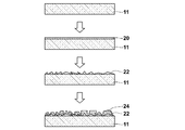
- FIG. 1 shows a process for manufacturing a photoelectric field enhancement substrate according to an embodiment of the photoelectric field enhancement device of the present invention, and is a sectional view for each process.
- a plate-like transparent substrate 11 is prepared, and the transparent substrate 11 is washed with acetone and methanol. Thereafter, as a thin film forming process, aluminum 20 is deposited on the surface of the transparent substrate 11 as a first metal by a thickness of about several tens of nm by sputtering.
- the transparent substrate 11 with the aluminum 20 is immersed in boiling pure water and taken out after a few minutes (about 5 minutes).
- the aluminum 20 becomes transparent and becomes a transparent fine uneven structure layer 22 made of a buyer-mite layer or a boehmite layer constituting the fine uneven structure.
- a second metal is deposited on the fine concavo-convex structure layer 22 as a metal layer manufacturing step.
- the photoelectric field enhancing substrate 1 in which the metal fine uneven structure 24 is generated on the fine uneven structure layer 22 can be produced.
- a plate-like substrate is used as the substrate, but a substrate having an arbitrary shape is applicable.
- the first metal to be hydrothermally reacted in the fine concavo-convex structure layer manufacturing step aluminum is given, but a metal oxide such as alumina (Al (OH) 3 ) may be used instead.
- Aluminum and alumina form a fine concavo-convex structure with a complex triangular pyramid structure consisting of either buyerite (Al [OH] 3 ) or boehmite (AlOOH) or both by hydrothermal reaction on the substrate. (See FIG. 3).
- a metal such as titanium (Ti) that forms a fine uneven structure by a hydrothermal reaction can be used.
- the method for forming the first metal or metal oxide on the substrate 11 is not limited to the sputtering method, and a heating vapor deposition method or a sol-gel method may be used.
- the hydrothermal reaction is not limited to boiling treatment, and the substrate on which the first metal is formed may be exposed to high-temperature water vapor so that the first metal reacts with high-temperature water vapor.
- the second metal constituting the metal fine concavo-convex structure layer 24 may be any metal that can generate localized plasmons when irradiated with excitation light.
- gold Au
- silver Au
- copper Cu
- Aluminum Al
- platinum Pt
- an alloy containing these as a main component Au or Ag is preferable.
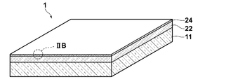
- FIG. 2A is a perspective view of the photoelectric field enhancement substrate 1 obtained by the above manufacturing process
- FIG. 2B is an enlarged view of a part IIB of the side surface of the photoelectric field enhancement substrate 1 shown in FIG. 2A.
- the photoelectric field enhancement substrate 1 includes a substrate 11, a fine concavo-convex structure layer 22 provided on the surface with a fine concavo-convex structure 23, and the fine concavo-convex structure 23.
- the metal fine uneven structure layer (metal layer) 24 formed on the surface of the metal fine uneven structure layer 25 on the surface of the metal fine uneven structure layer 24 is irradiated with light (hereinafter referred to as excitation light). Localized plasmon resonance is induced, and an enhanced photoelectric field is generated on the surface of the metal fine concavo-convex structure layer 24 by the localized plasmon resonance.
- the fine concavo-convex structure layer 22 made of a metal or metal oxide hydroxide such as a buyer-mite layer or a boehmite layer is transparent, and has various sizes (vertical angle sizes) and orientations as shown in FIG. 2B. However, it has a generally serrated cross section. According to the said manufacturing method, the fine concavo-convex structure layer 22 which has the fine concavo-convex structure 23 whose average pitch and depth are generally below the wavelength of excitation light can be obtained.
- the pitch is the distance between the vertices of the nearest adjacent convex portions across the concave portion
- the depth is the distance from the convex portion vertex to the bottom of the adjacent concave portion
- the metal layer 24 regardless of whether the excitation light is incident from the front or back of the substrate.
- a light enhancement field can be generated on the surface, and signal light such as Raman signal light can be detected from either the front or back of the substrate.
- the term “transparent” means that the transmittance is 50% or more with respect to the irradiated light and the light generated from the subject by the light. Note that the transmittance of these lights is preferably 75% or more, and more preferably 90% or more.
- the metal fine concavo-convex structure layer 24 may be formed along the surface of the fine concavo-convex structure layer 22 and may have a fine concavo-convex structure substantially the same as the fine concavo-convex structure 23, but as shown in FIG.
- the fine uneven structure 23 of the fine uneven structure layer 22 may have a fine uneven structure 25 having a different uneven shape on the surface.
- the fine concavo-convex structure layer 22 has substantially the same fine concavo-convex structure as the fine concavo-convex structure layer 23.
- the metal fine concavo-convex structure layer is formed. 2B has a fine concavo-convex structure in which the interval between adjacent convex portions is smaller than the interval between adjacent convex portions of the fine concavo-convex structure 23 corresponding between the adjacent convex portions as shown in FIG. 2B.
- the convex portions 24a are rounded and the distance between adjacent convex portions is smaller than when the metal is simply formed in a film shape along the fine concavo-convex structure 23 of the fine concavo-convex structure layer 22. Yes.
- the interval Wm between the convex portion 25a and the convex portion 25b adjacent to the convex portion 25a It is preferable that there is a portion that is smaller than the interval Wb between the convex portion 23a and the convex portion 23b of the structure 23.
- the interval Wm is half the depth Dm from the apex of the lower convex portion 25b of the adjacent convex portions 25a and 25b to the deepest portion 25c of the concave portion between both convex portions 25a and 25b. This is the distance between the convex portions 25a and 25b at the position of Dm / 2.
- the interval Wb is half the depth Db from the apex of the lower convex portion 23b of the adjacent convex portions 23a and 23b to the deepest portion 23c of the concave portion between both convex portions 23a and 23b. This is the distance between the convex portions 23a and 23b at the position of the depth Db / 2.
- the fine concavo-convex structure 25 of the metal fine concavo-convex structure layer 24 is such that at least one of the length in the direction perpendicular to the substrate and the length in the direction horizontal to the substrate is shorter than the wavelength of the excitation light. Any fine concavo-convex structure may be used as long as it can generate localized plasmons on the surface of the metal fine concavo-convex structure layer 24.
- the convex portions of the fine metal concavo-convex structure layer 24 are in the form of particles formed by aggregation of metals. It is particularly preferable that the granular convex portion has an aspect ratio (length in the direction perpendicular to the substrate / length in the horizontal direction on the substrate) of 0.5 or more. If it is granular, the surface area increases, so the number of analytes attached to the metal surface can be increased, leading to an increase in detection light.
- the average depth from the top of the convex portion of the fine concave-convex structure 25 of the metal fine concave-convex structure layer 24 to the bottom of the adjacent concave portion is 200 nm or less, and the average pitch between the vertices of the nearest convex portions separating the concave portions is 200 nm or less. Preferably there is.
- the metal fine concavo-convex structure layer 24 is formed on the fine concavo-convex structure layer 22 by vapor deposition as in the above-described manufacturing method, when the metal is vapor-deposited on the flat substrate, the thickness is 400 nm or less for gold and 90 nm or less for silver. By depositing with such a deposition amount, it is possible to obtain a metal fine concavo-convex structure that efficiently generates an enhanced photoelectric field.
- the distance between all adjacent convex portions of the fine concavo-convex structure in the formed metal fine concavo-convex structure layer is smaller than the interval between adjacent convex portions of the corresponding fine concavo-convex structure of the substrate.
- the effect of enhancing the photoelectric field becomes more prominent as the number of adjacent convex portions of the metal fine concavo-convex structure layer that is smaller than the interval between adjacent convex portions of the corresponding fine concavo-convex structure of the substrate increases.
- the second metal is only one layer, but two or more kinds of metals may be laminated.
- a dielectric may be laminated on the second metal.
- the film thickness of a dielectric material shall be 50 nm or less.
- 10 nm of SiO 2 is laminated on the metal microstructure layer.
- the fine metal concavo-convex structure layer may be formed by dispersing and disposing fine particles made of the second metal on the surface.
- the fine particles made of the second metal preferably have a diameter of 100 nm or less because a high photoelectric field enhancing effect can be obtained.
- Examples of the method for dispersing and fixing the metal fine particles include the following methods. 1) Metal fine particles are dispersed in an organic solvent, and the colloidal solution is cast on a boehmite substrate and dried. 2) A polycation or a cationic molecular film is adsorbed on a boehmite substrate, and metal fine particles are dispersed and fixed thereon by electrostatic interaction. 3) The boehmite substrate surface is modified with a thiol derivative, and metal fine particles are fixed by utilizing spontaneous bond formation between metal and sulfur. 4) Utilizing the fact that the metal fine particles are negatively charged, the metal fine particles are accumulated on the boehmite substrate by electrophoresis. By the method as described above, a metal fine uneven structure in which metal fine particles are dispersed and fixed on the fine uneven structure layer can be obtained.
- Method for producing photoelectric field enhancement substrate As the substrate 11, a glass substrate (BK-7; Corning Eagle 2000) was used. After ultrasonic cleaning (45 kHz) for 5 minutes with acetone and 5 minutes with methanol, a 25 nm thick aluminum 20 film was formed on the glass substrate 11 using a sputtering apparatus (manufactured by Canon Anelva). In addition, the aluminum thickness was measured using the surface shape measuring device (made by TENCOR), and it confirmed that thickness was 25 nm (+/- 10%).
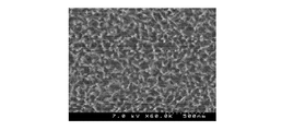
- FIG. 3 The result of having observed the surface of this transparent fine concavo-convex structure layer 22 in SEM (Hitachi S4100) is shown in FIG. In FIG. 3, convex portions are observed in white, and concave portions are observed in gray. Although the uneven pattern is irregular, it is uniformly formed on the entire surface, and the in-plane uniformity of the fine uneven structure is high. From the photograph of the boehmite layer surface shown in FIG. 3, it can be seen that the concavo-convex structure is composed of a number of ridge-shaped convex portions. The uneven structure cross section of the boehmite layer has a sawtooth shape as schematically shown in FIG. 2B.
- a sample in which a metal fine concavo-convex structure layer 24 was formed was formed by depositing Au on the surface of the transparent fine concavo-convex structure layer 22 by EB (Electric Beam) deposition for 30 nm.
- EB Electro Beam
- Au was deposited on the surface of the transparent fine concavo-convex structure layer 22 for 60, 90, 150, 250, and 400 nm, respectively, and Ag was deposited on each of 30, 60, 90, 150, 250, and 400 nm, respectively.
- a sample was made.
- the vapor deposition film thickness here is the same glass substrate as that for the sample, prepared for thickness measurement, part of the surface of the glass substrate for thickness measurement is masked with tape, and the sample substrate is placed in the vapor deposition chamber at the same time. It arrange
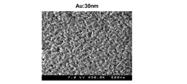
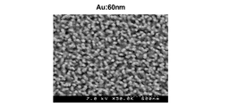
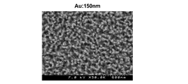
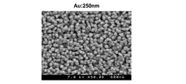
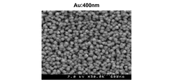
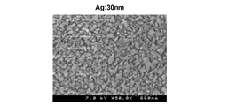
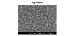
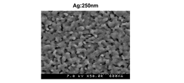
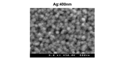
- FIGS. 4A to 4F SEM images of the surface of each sample are shown in FIGS. 4A to 4F for samples prepared by Au deposition, and FIGS. 5A to 5F for samples prepared by Ag deposition.
- the convex portions are aggregated and granulated, and the metal having a granular shape different from the fine uneven structure 25 on the surface of the buyerite or boehmite layer.
- a fine relief structure is formed.
- a metal granular shape is irradiated with light, a very strong photoelectric field called “hot spot” is generated between the particles, which is preferable as a photoelectric field enhancement substrate.
- the granularity increases as the film thickness increases, but the granular shape is maintained even at a film thickness of 400 nm as shown in FIG. 4F.
- the thickness of 150 to 400 nm has a granular structure larger than that of gold.
- Raman scattered light was detected using a microscopic Raman spectroscope (HR800).
- HR800 Raman spectroscope
- laser light having a peak wavelength of 785 nm was used and observed at a magnification of 20 times.
- the laser power immediately after the objective lens was 0.5 mW.
- the irradiation time was 10 seconds.
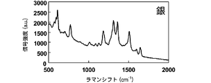
- FIG. 6 and 7 are graphs showing the Raman shift spectrum distribution detected by the microscopic Raman spectroscope, respectively.
- FIG. 6 shows the Raman shift spectrum distribution for a sample in which Au with a film thickness of 60 nm is deposited
- FIG. 7 shows the Raman shift spectrum distribution for a sample in which Ag with a film thickness of 60 nm is deposited.
- a very large Raman signal could be obtained with the sample manufactured using the method for manufacturing a photoelectric field enhancing substrate of the present invention shown in FIGS.
- samples with a thin vapor deposition film thickness (30 nm, 60 nm)
- a larger Raman signal could be obtained when silver was used as the second metal than when gold was used.
- FIG. 8 is a graph in which the peak intensity at 1360 cm ⁇ 1 after white noise removal is plotted with the gold film thickness as the horizontal axis, using the Raman shift spectrum distribution obtained for each sample subjected to Au deposition.
- the signal intensity increases with the film thickness when the gold film thickness is 30 to 90 nm.
- the convex portions of the gold film have a granular structure, and a large number of hot spots are generated by decreasing the distance between the convex portions. It is considered that the signal intensity increases.
- the signal intensity increases when the gold film thickness is 150 to 400 nm.
- the signal intensity is lower than that of the film thickness 30 to 90 nm. This is presumably because the enhancement of the photoelectric field deteriorated due to the increase in particle size or the contact between the particles and conduction.
- the intensity peak is obtained at a film thickness of 90 nm, the photoelectric field enhancement effect can be sufficiently obtained even at a film thickness of 150 to 400 nm, and an enhanced Raman signal is obtained.
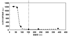
- FIG. 9 is a graph in which the peak intensity at 1360 cm ⁇ 1 after white noise removal is plotted with the silver film thickness as the horizontal axis, using the Raman shift spectrum distribution acquired for each of the samples subjected to Ag vapor deposition.
- the film thickness is 150 nm or more
- the signal intensity sharply decreases and almost no signal is obtained.
- the increase in the size of the photoelectric field deteriorated due to the increase in particle size or the contact and conduction between the particles.
- the silver layer is gradually flattened when the film thickness is thin, and further laminated on the flattened silver layer. it is conceivable that.
Landscapes
- Chemical & Material Sciences (AREA)
- Organic Chemistry (AREA)
- Engineering & Computer Science (AREA)
- Materials Engineering (AREA)
- Chemical Kinetics & Catalysis (AREA)
- Mechanical Engineering (AREA)
- Metallurgy (AREA)
- Inorganic Chemistry (AREA)
- Physics & Mathematics (AREA)
- Health & Medical Sciences (AREA)
- Life Sciences & Earth Sciences (AREA)
- Spectroscopy & Molecular Physics (AREA)
- General Physics & Mathematics (AREA)
- General Chemical & Material Sciences (AREA)
- Geochemistry & Mineralogy (AREA)
- Nuclear Medicine, Radiotherapy & Molecular Imaging (AREA)
- Analytical Chemistry (AREA)
- Biochemistry (AREA)
- General Health & Medical Sciences (AREA)
- Immunology (AREA)
- Pathology (AREA)
- Investigating, Analyzing Materials By Fluorescence Or Luminescence (AREA)
- Investigating Or Analysing Materials By Optical Means (AREA)
- Other Surface Treatments For Metallic Materials (AREA)
Abstract
【課題】ラマン散乱光を高い感度で検出し得る光電場増強デバイスを容易、かつ低コストに製造する。 【解決手段】基板(11)上に第1の金属または金属酸化物から成る薄膜(20)を形成し、この基板(11)上に形成された薄膜(20)を水熱反応させることにより、第1の金属または金属酸化物の水酸化物からなる微細凹凸構造層(22)を形成し、その後、微細凹凸構造層(22)の表面に、第2の金属から成る金属微細凹凸構造層(24)を形成する。
Description
本発明は、局在プラズモンを誘起しうる微細な金属凹凸構造を備えた光電場増強デバイスの製造方法に関するものである。
金属表面における局在プラズモン共鳴現象による電場増強効果を利用したセンサデバイスやラマン分光用デバイス等の電場増強デバイスが知られている。ラマン分光法は、物質に単波長光を照射して得られる散乱光を分光して、ラマン散乱光のスペクトル(ラマンスペクトル)を得る方法であり、物質の同定等に利用されている。
ラマン分光法には、微弱なラマン散乱光を増強するために、表面増強ラマン(SERS: Surface Enhanced Raman Scattering)と呼ばれる、局在プラズモン共鳴によって増強された光電場を利用したラマン分光法がある(非特許文献1参照)。これは、金属体、特に表面にナノオーダの凹凸を有する金属体に物質を接触させた状態で光を照射すると、局在プラズモン共鳴による光電場増強が生じ、金属体表面に接触された試料のラマン散乱光強度が増強されるという原理を利用するものである。被検体を担持する担体(基板)として、表面に金属凹凸構造を備えた基板を用いることにより表面増強ラマン分光法を実施することができる。
表面に金属微細凹凸構造を備えた基板としては、Si基板の表面に凹凸を設け、その凹凸面に金属膜を形成した基板が主に用いられている(特許文献1から3参照)。
また、Al基板の表面を陽極酸化して一部を金属酸化物層(Al2O3)とし、陽極酸化の過程で金属酸化物層内部に自然形成され、金属酸化物層の表面において開口した複数の微細孔内に、金属が充填された基板も提案されている(特許文献4参照)。
Optics Express Vol.17, No.2118556
光リソグラフィーおよびエッチングを用いて、微細凹凸構造を形成している特許文献1~3や、陽極酸化を用いている特許文献4では、微細凹凸構造作製や金属凹凸構造作製方法が複雑かつ大面積化が困難なため、単位面積当たりの基板コストが高くなると考えられる。また、複数の凹凸から成る液体容器などの複雑な基板に対し、上述のような金属凹凸構造を作製することは非常に困難であった。
本発明は、上記事情に鑑みてなされたものであって、任意の形状の基板に、比較的大面積に、低コストで光電場増強デバイスを作製する方法を提供するものである。
本発明の光電場増強デバイスの作製方法は、基板上に第1の金属または金属酸化物から成る薄膜を形成する薄膜形成工程と、
前記基板上に形成された薄膜を水熱反応させることにより、前記第1の金属または前記金属酸化物の水酸化物からなる微細凹凸構造層を形成する微細凹凸構造層作製工程と、
該微細凹凸構造層の表面に、第2の金属から成る金属微細凹凸構造層を形成する金属層作製工程とを含むことを特徴とする。
前記基板上に形成された薄膜を水熱反応させることにより、前記第1の金属または前記金属酸化物の水酸化物からなる微細凹凸構造層を形成する微細凹凸構造層作製工程と、
該微細凹凸構造層の表面に、第2の金属から成る金属微細凹凸構造層を形成する金属層作製工程とを含むことを特徴とする。
前記金属層作製工程において、前記金属微細凹凸構造層として前記微細凹凸構造とは形状が異なる凹凸構造を表面に有する金属層を形成することが好ましい。
第2の金属としては、金(Au),銀(Ag),銅(Cu),アルミニウム(Al)、プラチナ(Pt)またはこれらを主成分とする合金であることが好ましい。特には、AuあるいはAgが好ましい。
前記金属層作製工程は、前記微細凹凸構造層の表面に、第2の金属からなる金属層を形成する方法として、金属蒸着法を用いた金属蒸着工程とすることができる。
蒸着法で、第2の金属として金を用いた場合、蒸着膜厚を30nm以上とすることが望ましい。
蒸着法で、第2の金属として銀を用いた場合、蒸着膜厚を150nm以下とすることが、望ましい。
前記金属層作製工程の後に、前記第2の金属からなる金属微細構造層上に該第2の金属とは異なる第3の金属および誘電体のいずれか一方を積層する積層工程を含んでもよい。
また、前記金属層作製工程を、前記微細凹凸構造層の表面に前記第2の金属からなる金属微粒子を分散させる、金属微粒子分散工程としてもよい。
前記金属微粒子としては、直径100nm以下のものを用いることが好ましい。
前記第1の金属としてアルミニウム(Al)、前記金属酸化物としてアルミナ(Al2O3)を用いることができる。
前記水酸化物がバイヤーマイトおよびベーマイトの少なくとも一方からなることが望ましい。
本発明の光電場増強デバイスの製造方法は、基板上に第1の金属または金属酸化物を形成する薄膜形成工程と、基板上に形成された薄膜を水熱反応させることにより前記第1の金属または前記金属酸化物の水酸化物からなる微細凹凸構造層を形成工程と、微細凹凸構造層の表面に、第2の金属から成る金属微細凹凸構造層を形成する金属層作製工程との簡単な工程で、数十ナノメートルサイズの金属微細凹凸構造を表面に備えた光電場増強デバイスを得ることができる。
このような非常に簡素な工程により光電場増強デバイスを得ることができるので、従来のデバイスと比較して製造コストを大幅に抑えることができる。
また、それぞれの工程が、比較的大面積の基板や任意の形状を有する基板にも適応可能であり、大面積かつ任意形状の光電場増強デバイスが作製可能となる。
また、それぞれの工程が、比較的大面積の基板や任意の形状を有する基板にも適応可能であり、大面積かつ任意形状の光電場増強デバイスが作製可能となる。
本発明の製造方法により得られた光電場増強デバイスは、表面の金属微細凹凸に光が照射されると、金属から成る微細凹凸構造表面に局在プラズモンを効果的に誘起することができ、この局在プラズモンによる光電場増強効果を生じさせることができる。また、この光電場増強デバイス上に被検体を配置して、該被検体が配置された領域に光が照射されることにより被検体から生じる光は光電場増強効果により増強されたものとなり、高感度に光を検出することが可能となる。表面増強ラマン基板としても好適に用いることができ、ラマン信号を効果的に増強させることができ、高感度化を図ることができる。
以下、図面を参照して本発明の光電場増強デバイスの製造方法の実施形態について説明する。
図1は、本発明の光電場増強デバイスの一実施形態に係る光電場増強基板の製造工程を示すものであり、各工程毎の断面図である。
まず、板状の透明基板11を用意し、透明基板11をアセトンおよびメタノールで洗浄する。その後、薄膜形成工程として、透明基板11の表面にスパッタ法により第1の金属としてアルミニウム20を数十nm程度成膜する。
その後、微細凹凸構造層作製工程として、沸騰させた純水の中に、アルミニウム20付き透明基板11を浸水させ、数分(5分程度)後に取り出す。この煮沸処理(水熱反応)により、アルミニウム20は透明化し、微細凹凸構造を構成するバイヤーマイト層もしくはベーマイト層からなる透明な微細凹凸構造層22となる。
次に、金属層作製工程として、この微細凹凸構造層22上に第2の金属を蒸着する。
以上の処理により、微細凹凸構造層22上に金属微細凹凸構造24が生成されてなる光電場増強基板1を作製することができる。
上記においては基板として板状の基板を用いるものとしたが、任意の形状の基板であっても適応可能である。
微細凹凸構造層作製工程において水熱反応させる第1の金属としてはアルミニウムが挙げられるが、これに代えてアルミナ(Al(OH)3)のような金属酸化物を用いてもよい。アルミニウムおよびアルミナは、水熱反応させることにより、バイヤーマイト(Al[OH]3)またはベーマイト(AlOOH)のいずれか、または両方からなる、複雑な三角錐構造を有する微細凹凸構造を基板上に形成することができる(図3参照)。
なお、第1の金属としては、アルミニウムの他、チタン(Ti)など、同様に水熱反応により微細凹凸構造を形成する金属を用いることができる。
なお、第1の金属としては、アルミニウムの他、チタン(Ti)など、同様に水熱反応により微細凹凸構造を形成する金属を用いることができる。
また、第1の金属あるいは金属酸化物を基板11に成膜する方法は、スパッタ法に限らず、加熱蒸着法やゾルゲル法を用いてもよい。
水熱反応としては、煮沸処理に限らず、第1の金属が成膜された基板を高温の水蒸気に曝して第1の金属を高温の水蒸気と反応させる処理を行ってもよい。
水熱反応としては、煮沸処理に限らず、第1の金属が成膜された基板を高温の水蒸気に曝して第1の金属を高温の水蒸気と反応させる処理を行ってもよい。
金属微細凹凸構造層24を構成する第2の金属は、励起光の照射を受けて局在プラズモンを生じうる金属であればよいが、例えば、金(Au)、銀(Ag)、銅(Cu)、アルミニウム(Al)、プラチナ(Pt)、またはこれらを主成分とする合金である。特には、AuあるいはAgが好ましい。
図2Aは、上記の製造工程により得られる光電場増強基板1の斜視図であり、図2Bは、図2Aに示した光電場増強基板1の側面の一部IIBの拡大図である。
図2Aおよび図2Bに示すように、光電場増強基板1は、基板11と、基板11上に設けられた、表面に微細凹凸構造23を備えた微細凹凸構造層22と、その微細凹凸構造23の表面に形成された金属微細凹凸構造層(金属層)24とからなり、金属微細凹凸構造層24の表面の微細凹凸構造25に照射された光(以下において、励起光とする。)により、局在プラズモン共鳴が誘起され、この局在プラズモン共鳴により金属微細凹凸構造層24の表面に増強された光電場を生じさせるものである。
バイヤーマイト層またはベーマイト層などの金属または金属酸化物の水酸化物からなる微細凹凸構造層22は、透明であり、図2Bに示すように、大きさ(頂角の大きさ)や向きはさまざまであるが概ね鋸歯状の断面を有している。上記製造方法によれば、平均ピッチおよび深さが概ね励起光の波長以下の微細凹凸構造23を有する微細凹凸構造層22を得ることができる。なおここで、微細凹凸構造23において、ピッチは凹部を隔てた最隣接凸部の頂点同士の距離であり、深さは凸部頂点から隣接する凹部の底部までの距離である。
なお、基板11としてガラスなどの透明基板を用い、バイヤーマイト層またはベーマイト層などの透明な微細凹凸構造層22を備えるものとすれば、基板の表裏いずれから励起光を入射させても金属層24表面に光増強場を生じさせることができ、また、ラマン信号光などの信号光を基板の表裏いずれからでも検出することができる。ここで、透明とは、照射される光、および該光により被検体から生じる光に対し、透過率が50%以上であることをいうものとする。なお、これらの光に対して、透過率は75%以上、さらには90%以上であることが好ましい。
金属微細凹凸構造層24は、微細凹凸構造層22の表面に沿って形成されてその微細凹凸構造23とほぼ同様の微細凹凸構造を有するものであってもよいが、図2Bに示すように、微細凹凸構造層22の微細凹凸構造23とは、異なる凹凸形状を有する微細凹凸構造25を表面に有するものであってもよい。
上記製造方法において、金属の蒸着膜厚を薄くすると、微細凹凸構造層22の微細凹凸構造23とほぼ同様の微細凹凸構造を有するものとなり、金属の蒸着膜厚を厚くすると、金属微細凹凸構造層24は、図2Bに示すように隣接凸部間の間隔がその隣接凸部間に対応する微細凹凸構造23の隣接凸部間の間隔よりも小さい微細凹凸構造を有するものとなる。金属微細凹凸構造層24は、微細凹凸構造層22の微細凹凸構造23に沿って単に金属を膜状に形成した場合よりも凸部24aが丸みを帯び、隣接凸部間の距離が小さくなっている。
金属微細凹凸構造層24の微細凹凸構造25に、図2Bに示すように、凸部25aとそれに隣接する凸部25bとの間隔Wmが、これらの凸部25a、25bに対応する基板の微細凹凸構造23の凸部23aと凸部23bとの間隔Wbよりも小さくなっている部分があることが好ましい。ここで、間隔Wmは、隣接する凸部25aと凸部25bのうち低い方の凸部25bの頂点から両凸部25a、25b間の凹部の最も深い部分25cまでの深さDmの半分の深さDm/2の位置での凸部25a、25b間の距離である。また、同様に間隔Wbは、隣接する凸部23aと凸部23bのうち低い方の凸部23bの頂点から両凸部23a、23b間の凹部の最も深い部分23cまでの深さDbの半分の深さDb/2の位置での凸部23a、23b間の距離である。
金属微細凹凸構造層24の微細凹凸構造25は、その凹凸の凸部の基板に垂直な方向の長さおよび基板に水平な方向の長さの少なくとも一方が励起光の波長より短いものとなる程度の微細な凹凸構造であり、金属微細凹凸構造層24の表面に局在プラズモンを生じうるものであればよい。
また、金属微細凹凸構造層24の凸部は金属が凝集してなる粒子状であることが望ましい。粒状の凸部は、アスペクト比(基板に垂直方向の長さ/基板に水平方向の長さ)が0.5以上であることが特に好ましい。粒状であれば表面積が大きくなることから、金属表面に付着する被検体数を増加させることができ、検出光の増加に繋がる。
なお、金属微細凹凸構造層24の微細凹凸構造25の凸部頂点から隣接する凹部の底部までの平均深さが200nm以下、凹部を隔てた最隣接凸部の頂点同士の平均ピッチが200nm以下であることが好ましい。
微細凹凸構造層22上に上述の製造方法のように蒸着により金属微細凹凸構造層24を形成する場合、平面基板上に金属を蒸着した場合に金では400nm以下、銀では90nm以下の厚みとなるような蒸着量で蒸着することにより、効率よく増強された光電場を生じさせる金属微細凹凸構造を得ることができる。
なお、形成された金属微細凹凸構造層における微細凹凸構造の全ての隣接凸部間が、対応する基板の微細凹凸構造の隣接凸部間の間隔よりも小さいものである必要はない。一方で、対応する基板の微細凹凸構造の隣接凸部間の間隔よりも小さい金属微細凹凸構造層の隣接凸部間が多いほど、光電場増強の効果は顕著なものとなる。
特に、金属微細凹凸構造25の隣接凸部同士が間隔が20nm以下で近接している場合、光の照射によりこの凸部間の隙間においてホットスポットと呼ばれる非常に強い光電場増強場が生成されるため、隣接凸部間の距離が20nm以下の箇所が多数存在することが好ましい。
特に、金属微細凹凸構造25の隣接凸部同士が間隔が20nm以下で近接している場合、光の照射によりこの凸部間の隙間においてホットスポットと呼ばれる非常に強い光電場増強場が生成されるため、隣接凸部間の距離が20nm以下の箇所が多数存在することが好ましい。
上記実施形態において、第2の金属は一層のみとしているが2種類以上の金属を積層させてもよい。また、第2の金属上に誘電体を積層してもよい。このように、2種類以上の金属を積層させたり、第2の金属上に誘電体を積層することにより、干渉効果や酸化防止効果を持たせることができる。すなわち、光学干渉による効果により、層構造の厚みが光のある位相と合致した場合、層構造に光が閉じ込められ、さらなる光電場増強効果を生じさせることができる。また、例えば、第2の金属として銀層を設け、その上に金層を積層することにより、銀の酸化を抑制することができる。
なお、第2の金属からなる金属微細凹凸構造層上に誘電体を積層する場合、誘電体の膜厚は50nm以下とすることが望ましい。例えば、金属微細構造層上にSiO2を10nm積層する。
なお、第2の金属からなる金属微細凹凸構造層上に誘電体を積層する場合、誘電体の膜厚は50nm以下とすることが望ましい。例えば、金属微細構造層上にSiO2を10nm積層する。
金属微細構造層の形成方法として、上記実施形態においては蒸着法を用いて、微細凹凸構造層の表面に金属を蒸着させる方法を説明したが、金属微細構造層の作製工程として、微細凹凸構造層の表面に第2の金属からなる微粒子を分散配置させることにより金属微細凹凸構造層を形成するようにしてもよい。
第2の金属からなる微粒子としては直径が100nm以下であることが、高い光電場増強効果を得ることができ好ましい。
第2の金属からなる微粒子としては直径が100nm以下であることが、高い光電場増強効果を得ることができ好ましい。
金属微粒子を分散させて固定させる方法としては、例えば以下の方法が挙げられる。
1)金属微粒子を有機溶媒に分散させコロイド溶液をベーマイト基板にキャストし乾燥させる。
2)ベーマイト基板上にポリカチオンやカチオン性分子膜を吸着させ、その上に静電気相互作用によって金属微粒子を分散、固定する。
3)ベーマイト基板表面をチオール誘導体で修飾し、金属―イオウ間の自発的な結合形成を利用して金属微粒子を固定させる。
4)金属微粒子が負に帯電していることを利用して、電気泳動法によりベーマイト基板上に金属微粒子を集積する。
以上のような方法により、金属微粒子が微細凹凸構造層上に分散固定されてなる金属微細凹凸構造を得ることができる。
1)金属微粒子を有機溶媒に分散させコロイド溶液をベーマイト基板にキャストし乾燥させる。
2)ベーマイト基板上にポリカチオンやカチオン性分子膜を吸着させ、その上に静電気相互作用によって金属微粒子を分散、固定する。
3)ベーマイト基板表面をチオール誘導体で修飾し、金属―イオウ間の自発的な結合形成を利用して金属微粒子を固定させる。
4)金属微粒子が負に帯電していることを利用して、電気泳動法によりベーマイト基板上に金属微粒子を集積する。
以上のような方法により、金属微粒子が微細凹凸構造層上に分散固定されてなる金属微細凹凸構造を得ることができる。
以下、本発明の光電場増強デバイスの実施形態である光電場増強基板1の具体的な作製例および測定用サンプルを用いてラマン分光測定を行った結果を説明する。
「光電場増強基板の作製方法」
基板11として、ガラス基板(BK-7;コーニング社製Eagle2000)を用いた。
アセトン5分、メタノール5分の超音波洗浄(45kHz)を行った後、ガラス基板11にスパッタ装置(キャノンアネルバ社製)を用いてアルミニウム20を25nm厚成膜した。なお、表面形状測定器(TENCOR社製)を用いて、アルミニウム厚みを測定し、厚みは25nm(±10%)であることを確認した。
基板11として、ガラス基板(BK-7;コーニング社製Eagle2000)を用いた。
アセトン5分、メタノール5分の超音波洗浄(45kHz)を行った後、ガラス基板11にスパッタ装置(キャノンアネルバ社製)を用いてアルミニウム20を25nm厚成膜した。なお、表面形状測定器(TENCOR社製)を用いて、アルミニウム厚みを測定し、厚みは25nm(±10%)であることを確認した。
その後、ウォーターバス(西精機株式会社)の中に純水を用意して、沸騰させた。
その沸騰水の中にアルミニウム20付きガラス基板11を浸水させて、5分間経過後に取り出した。この際、アルミニウム20付きガラス基板11を沸騰水に浸水させて1-2分程度でアルミニウムが透明化したことを確認した。この透明化は煮沸処理により、アルミニウム20がバイヤーマイトもしくはベーマイトとからなる微細凹凸構造層22となったためである。
その沸騰水の中にアルミニウム20付きガラス基板11を浸水させて、5分間経過後に取り出した。この際、アルミニウム20付きガラス基板11を沸騰水に浸水させて1-2分程度でアルミニウムが透明化したことを確認した。この透明化は煮沸処理により、アルミニウム20がバイヤーマイトもしくはベーマイトとからなる微細凹凸構造層22となったためである。
この透明な微細凹凸構造層22の表面を、SEM(日立製S4100)にて観察した結果を図3に示す。図3中に白く観察されるのが凸部、灰色に観察されるのが凹部である。凹凸のパターンは不規則であるが、全面に一様に形成されており、微細凹凸構造の面内均一性は高い。図3に示すベーマイト層表面の写真から、凹凸構造は、多数の峰状の凸部から構成されていることが分かる。なお、このベーマイト層の凹凸構造断面は図2Bに模式的に示しているように鋸歯状である。
最後に、透明な微細凹凸構造層22の表面にAuをEB(Electric Beam)蒸着により30nm分成膜して、金属微細凹凸構造層24を形成したサンプルを作製した。なお、同様にして透明な微細凹凸構造層22の表面にAuを60、90、150、250、400nm分それぞれ蒸着したサンプル、およびAgを30、60、90、150、250、400nm分それぞれ蒸着したサンプルを作製した。ここでの蒸着膜厚は、サンプルとは別途同じガラス基板を厚み計測用に用意して、厚み計測用のガラス基板の表面の一部をテープでマスクし、サンプル用の基板と同時に蒸着室に配置して蒸着を行い、蒸着後に厚み計測用のガラス基板からテープは剥がし、テープを剥がした金属が蒸着されていない表面から蒸着された金属表面までの厚みを測定したものである。
各サンプル表面のSEM画像を、Au蒸着により作製したサンプルについては図4A~図4Fに、Ag蒸着により作製したサンプルについては図5A~図5Fに示す。
Au蒸着の場合、図4A~図4Fに示されるように、蒸着厚みが増していくと、凸部が凝集、粒状化し、バイヤーマイトまたはベーマイト層表面の微細凹凸構造25とは異なる粒状形状の金属微細凹凸構造が形成される。このような金属の粒状形状に光が照射された場合、粒状間に「ホットスポット」と呼ばれる非常に強い光電場が生成されるため、光電場増強基板として好ましい。膜厚が厚くなるにつれて粒状が大きくなるが、図4Fに示すように膜厚400nmにおいても粒状形状は維持されている。
Agの場合、図5A~図5Cに示されるように、厚み30~90nmにおいて、厚みが大きくなるにつれて銀が徐々に凝集し、徐々に大きな島状の構造になっており、銀膜層が徐々に平坦化していると考えられる。また、図5D~図5Fに示されるように、厚み150~400nmにおいては、金よりも大きな粒状構造となっている。
(ラマン散乱光の測定)
上記方法で作製した光電場増強基板の各サンプル上にそれぞれ被検体としてエタノールにローダミン6Gを溶かした溶液100μMを滴下し、乾燥させた測定サンプルを用い、ラマン散乱光を測定した。
上記方法で作製した光電場増強基板の各サンプル上にそれぞれ被検体としてエタノールにローダミン6Gを溶かした溶液100μMを滴下し、乾燥させた測定サンプルを用い、ラマン散乱光を測定した。
ラマン散乱光は、顕微ラマン分光装置(HR800)を用いて検出した。励起光としては、ピーク波長785nmのレーザ光を用い、倍率20倍で観測した。対物レンズ直後のレーザパワーは0.5mWであった。また、照射時間は10秒とした。
図6、図7は、それぞれ顕微ラマン分光装置により検出されたラマンシフトスペクトル分布を示すグラフである。図6は、膜厚60nmのAuを蒸着したサンプルについて、図7は膜厚60nmのAgを蒸着したサンプルについてのラマンシフトスペクトル分布を示す。
図6、7に示す、本発明の光電場増強基板の作製方法を用いて作製したサンプルでは、非常に大きなラマン信号を得ることができた。なお、蒸着膜厚の薄いサンプル(30nm、60nm)では、第2の金属として銀を用いた方が金を用いた場合より大きなラマン信号を得ることができた。
図8は、Au蒸着を行った各サンプルのそれぞれについて取得したラマンシフトスペクトル分布を用い、ホワイトノイズ除去後の1360cm-1のピーク強度を金膜厚を横軸としてプロットしたグラフである。
図8に示すように、金膜厚が30~90nmにおいては、膜厚と共に信号強度が増加していることが分かる。これは、図4A~図4CのSEM画像から明らかなように膜厚増加に伴い、金膜の凸部が粒状構造となり、凸部間の距離が小さくなることによりホットスポットが多数発生することから、信号強度が増加するものと考えられる。一方、図8に示すように、金膜厚が150~400nmにおいては、信号強度が膜厚30~90nmと比較して低下している。これは、粒子サイズが大きくなっていることや粒子同士が接触し導通してしまうことにより、光電場増強度が劣化したためと考えられる。膜厚90nmで強度ピークとなっているが、膜厚150~400nmにおいても十分に光電場増強効果を得ることはでき、増強ラマン信号は得られている。
図9は、Ag蒸着を行った各サンプルのそれぞれについて取得したラマンシフトスペクトル分布を用い、ホワイトノイズ除去後の1360cm-1のピーク強度を銀膜厚を横軸としてプロットしたグラフである。
銀の場合は、膜厚が150nm以上になると、急激に信号強度が減少し、ほとんど信号が得られていないことが分かる。これは、金の場合と同様に、粒子サイズが大きくなっていることや粒子同士が接触し導通してしまうことにより、光電場増強度が劣化したためと考えられる。さらに銀の場合は、膜厚が薄い時点で銀層が徐々に平坦化し、平坦化してきた銀層上にさらに積層されたために、銀層が導通し安く、光電場増強度が大幅に劣化したためと考えられる。
Claims (11)
- 基板上に第1の金属または金属酸化物から成る薄膜を形成する薄膜形成工程と、
前記基板上に形成された薄膜を水熱反応させることにより、前記第1の金属または前記金属酸化物の水酸化物からなる微細凹凸構造層を形成する微細凹凸構造層作製工程と、
該微細凹凸構造層の表面に、第2の金属から成る金属微細凹凸構造層を形成する金属層作製工程とを含むことを特徴とする光電場増強デバイスの製造方法。 - 前記金属層作製工程において、前記金属微細凹凸構造層として前記微細凹凸構造とは形状が異なる凹凸構造を表面に有する金属層を形成することを特徴とする請求項1記載の光電場増強デバイスの製造方法。
- 前記第2の金属が、金、銀、銅、アルミニウムまたはプラチナであることを特徴とする請求項1または2項記載の光電場増強デバイスの製造方法。
- 前記金属層作製工程が、前記微細凹凸構造層の表面に前記第2の金属を蒸着する金属蒸着工程であることを特徴とする請求項1から3いずれか1項記載の光電場増強デバイスの製造方法。
- 前記第2の金属が金であり、蒸着膜厚が30nm以上であることを特徴とする請求項4記載の光電場増強デバイスの製造方法。
- 前記第2の金属が銀であり、蒸着膜厚が150nm以下であることを特徴とする請求項4記載の光電場増強デバイスの製造方法。
- 前記金属層作製工程の後に、前記第2の金属からなる金属微細構造層上に該第2の金属とは異なる第3の金属および誘電体のいずれか一方を積層する積層工程を含むことを特徴とする請求項1から6いずれか1項記載の光電場増強デバイスの製造方法。
- 前記金属層作製工程が、前記微細凹凸構造層の表面に前記第2の金属からなる金属微粒子を分散させる、金属微粒子分散工程であることを特徴とする請求項1から3いずれか1項記載の光電場増強デバイスの製造方法。
- 前記金属微粒子の直径が100nm以下であることを特徴とする請求項8記載の光電場増強デバイスの製造方法。
- 前記第1の金属がアルミニウムであり、前記金属酸化物がアルミナであることを特徴とする請求項1から9いずれか1項記載の光電場増強デバイスの製造方法。
- 前記水酸化物がバイヤーマイトおよびベーマイトの少なくとも一方からなることを特徴とする請求項1から10いずれか1項記載の光電場増強デバイスの製造方法。
Priority Applications (3)
| Application Number | Priority Date | Filing Date | Title |
|---|---|---|---|
| CN201280016792.0A CN103492861B (zh) | 2011-03-31 | 2012-03-26 | 光电场增强器件的制造方法 |
| EP12764916.8A EP2693202B1 (en) | 2011-03-31 | 2012-03-26 | Manufacturing method for optical-electric-field enhancement device |
| US14/041,877 US20140034235A1 (en) | 2011-03-31 | 2013-09-30 | Method for producing optical electrical field enhancing device |
Applications Claiming Priority (2)
| Application Number | Priority Date | Filing Date | Title |
|---|---|---|---|
| JP2011077868A JP5801587B2 (ja) | 2011-03-31 | 2011-03-31 | 光電場増強デバイスの製造方法 |
| JP2011-077868 | 2011-03-31 |
Related Child Applications (1)
| Application Number | Title | Priority Date | Filing Date |
|---|---|---|---|
| US14/041,877 Continuation US20140034235A1 (en) | 2011-03-31 | 2013-09-30 | Method for producing optical electrical field enhancing device |
Publications (1)
| Publication Number | Publication Date |
|---|---|
| WO2012132385A1 true WO2012132385A1 (ja) | 2012-10-04 |
Family
ID=46930161
Family Applications (1)
| Application Number | Title | Priority Date | Filing Date |
|---|---|---|---|
| PCT/JP2012/002072 Ceased WO2012132385A1 (ja) | 2011-03-31 | 2012-03-26 | 光電場増強デバイスの製造方法 |
Country Status (5)
| Country | Link |
|---|---|
| US (1) | US20140034235A1 (ja) |
| EP (1) | EP2693202B1 (ja) |
| JP (1) | JP5801587B2 (ja) |
| CN (1) | CN103492861B (ja) |
| WO (1) | WO2012132385A1 (ja) |
Families Citing this family (9)
| Publication number | Priority date | Publication date | Assignee | Title |
|---|---|---|---|---|
| JP6145861B2 (ja) | 2012-08-15 | 2017-06-14 | 富士フイルム株式会社 | 光電場増強デバイス、光測定装置および方法 |
| JP2014190834A (ja) * | 2013-03-27 | 2014-10-06 | Fujifilm Corp | 光電場増強デバイスおよびその製造方法 |
| JP6229387B2 (ja) * | 2013-09-12 | 2017-11-15 | 大日本印刷株式会社 | 光学部材、及びその製造方法 |
| JP6337127B2 (ja) * | 2014-08-27 | 2018-06-06 | 富士フイルム株式会社 | 光電場増強デバイスおよび光電場増強デバイスの製造方法 |
| CN105158228B (zh) * | 2015-07-30 | 2018-07-20 | 西北大学 | 基于勃姆石纳米薄膜的sers基底及制备方法 |
| EP3350598A4 (en) | 2015-09-17 | 2019-03-27 | Gerhard Maale | SENSOR DEVICE FOR BIOSENSING AND OTHER APPLICATIONS |
| CN106093007A (zh) * | 2016-06-20 | 2016-11-09 | 上海理工大学 | 一种表面增强拉曼散射基底及其制备方法 |
| CN108275651A (zh) * | 2018-01-22 | 2018-07-13 | 临沂大学 | 一种表面增强拉曼散射基底的制备方法 |
| FR3158725B1 (fr) * | 2024-01-31 | 2026-01-16 | Saint Gobain | Substrat de vitrage |
Citations (11)
| Publication number | Priority date | Publication date | Assignee | Title |
|---|---|---|---|---|
| JPS6148124B2 (ja) * | 1977-02-18 | 1986-10-22 | Minnesota Mining & Mfg | |
| JP2005172569A (ja) | 2003-12-10 | 2005-06-30 | Fuji Photo Film Co Ltd | 微細構造体、微細構造体の作製方法、ラマン分光方法および装置 |
| JP2006514286A (ja) | 2003-02-18 | 2006-04-27 | インテル・コーポレーション | 活性表面増強ラマン分光分析(sers)の基体としての金属被覆ナノ結晶シリコン |
| JP2006145230A (ja) | 2004-11-16 | 2006-06-08 | Canon Inc | 被分析物担体およびその製造方法 |
| JP2007240361A (ja) * | 2006-03-09 | 2007-09-20 | Sekisui Chem Co Ltd | 局在プラズモン増強センサ |
| JP2009109395A (ja) * | 2007-10-31 | 2009-05-21 | Fujifilm Corp | 微細構造体の作製方法、微細構造体、ラマン分光用デバイス、ラマン分光装置、分析装置、検出装置、および質量分析装置 |
| JP2009236830A (ja) * | 2008-03-28 | 2009-10-15 | Sumitomo Precision Prod Co Ltd | 被分析物担体、及び、その製造方法 |
| JP4347801B2 (ja) | 2002-06-12 | 2009-10-21 | インテル・コーポレーション | 活性表面増強ラマン分光(sers)基板としての金属被覆ナノ結晶性シリコン |
| JP2012063294A (ja) * | 2010-09-17 | 2012-03-29 | Fujifilm Corp | 光電場増強デバイスを用いた光の測定方法および測定装置 |
| JP2012063293A (ja) * | 2010-09-17 | 2012-03-29 | Fujifilm Corp | 光電場増強デバイス |
| JP2012132743A (ja) * | 2010-12-21 | 2012-07-12 | Fujifilm Corp | 光電場増強デバイスおよび光検出装置 |
Family Cites Families (7)
| Publication number | Priority date | Publication date | Assignee | Title |
|---|---|---|---|---|
| US4252843A (en) * | 1977-02-18 | 1981-02-24 | Minnesota Mining And Manufacturing Company | Process for forming a microstructured transmission and reflectance modifying coating |
| JPH09202649A (ja) * | 1996-01-24 | 1997-08-05 | Central Glass Co Ltd | 花弁状透明アルミナ膜及びその形成法 |
| US6406777B1 (en) * | 2000-06-14 | 2002-06-18 | The United States Of America As Represented By The Secretary Of The Navy | Metal and glass structure for use in surface enhanced Raman spectroscopy and method for fabricating same |
| JP4639241B2 (ja) * | 2007-02-20 | 2011-02-23 | キヤノン株式会社 | 光学用部材、それを用いた光学系及び光学用部材の製造方法 |
| KR20120022754A (ko) * | 2009-03-04 | 2012-03-12 | 유키 하세가와 | 표면 증강 라먼 산란 활성 측정 기판 |
| US8427639B2 (en) * | 2009-05-07 | 2013-04-23 | Nant Holdings Ip, Llc | Surfaced enhanced Raman spectroscopy substrates |
| US20110128535A1 (en) * | 2009-11-30 | 2011-06-02 | David Eugene Baker | Nano-Structured Substrates, Articles, and Methods Thereof |
-
2011
- 2011-03-31 JP JP2011077868A patent/JP5801587B2/ja not_active Expired - Fee Related
-
2012
- 2012-03-26 EP EP12764916.8A patent/EP2693202B1/en not_active Not-in-force
- 2012-03-26 WO PCT/JP2012/002072 patent/WO2012132385A1/ja not_active Ceased
- 2012-03-26 CN CN201280016792.0A patent/CN103492861B/zh not_active Expired - Fee Related
-
2013
- 2013-09-30 US US14/041,877 patent/US20140034235A1/en not_active Abandoned
Patent Citations (11)
| Publication number | Priority date | Publication date | Assignee | Title |
|---|---|---|---|---|
| JPS6148124B2 (ja) * | 1977-02-18 | 1986-10-22 | Minnesota Mining & Mfg | |
| JP4347801B2 (ja) | 2002-06-12 | 2009-10-21 | インテル・コーポレーション | 活性表面増強ラマン分光(sers)基板としての金属被覆ナノ結晶性シリコン |
| JP2006514286A (ja) | 2003-02-18 | 2006-04-27 | インテル・コーポレーション | 活性表面増強ラマン分光分析(sers)の基体としての金属被覆ナノ結晶シリコン |
| JP2005172569A (ja) | 2003-12-10 | 2005-06-30 | Fuji Photo Film Co Ltd | 微細構造体、微細構造体の作製方法、ラマン分光方法および装置 |
| JP2006145230A (ja) | 2004-11-16 | 2006-06-08 | Canon Inc | 被分析物担体およびその製造方法 |
| JP2007240361A (ja) * | 2006-03-09 | 2007-09-20 | Sekisui Chem Co Ltd | 局在プラズモン増強センサ |
| JP2009109395A (ja) * | 2007-10-31 | 2009-05-21 | Fujifilm Corp | 微細構造体の作製方法、微細構造体、ラマン分光用デバイス、ラマン分光装置、分析装置、検出装置、および質量分析装置 |
| JP2009236830A (ja) * | 2008-03-28 | 2009-10-15 | Sumitomo Precision Prod Co Ltd | 被分析物担体、及び、その製造方法 |
| JP2012063294A (ja) * | 2010-09-17 | 2012-03-29 | Fujifilm Corp | 光電場増強デバイスを用いた光の測定方法および測定装置 |
| JP2012063293A (ja) * | 2010-09-17 | 2012-03-29 | Fujifilm Corp | 光電場増強デバイス |
| JP2012132743A (ja) * | 2010-12-21 | 2012-07-12 | Fujifilm Corp | 光電場増強デバイスおよび光検出装置 |
Non-Patent Citations (4)
| Title |
|---|
| JUNG-YEN YANG ET AL.: "Detection of Staphylococcus Aureus Using Hydrothermally Roughened Substrates", PROCEEDINGS OF THE 2009 IEEE 3RD INTERNATIONAL CONFERENCE ON NANO/MOLECULAR MEDICINE AND ENGINEERING, 18 October 2009 (2009-10-18), pages 210 - 214, XP031740300 * |
| JUNG-YEN YANG ET AL.: "Surface-Enhanced Raman Scattering Active Substrates", IEEE NANOTECHNOLOGY MAGAZINE, vol. 5, no. 1, 24 February 2011 (2011-02-24), pages 12 - 16, XP011348529 * |
| OPTICS EXPRESS, vol. 17, no. 21, pages 18556 |
| See also references of EP2693202A4 |
Also Published As
| Publication number | Publication date |
|---|---|
| JP2012211839A (ja) | 2012-11-01 |
| US20140034235A1 (en) | 2014-02-06 |
| CN103492861A (zh) | 2014-01-01 |
| JP5801587B2 (ja) | 2015-10-28 |
| EP2693202A4 (en) | 2014-09-03 |
| EP2693202B1 (en) | 2017-11-15 |
| CN103492861B (zh) | 2016-08-10 |
| EP2693202A1 (en) | 2014-02-05 |
Similar Documents
| Publication | Publication Date | Title |
|---|---|---|
| JP5801587B2 (ja) | 光電場増強デバイスの製造方法 | |
| JP5848013B2 (ja) | 光電場増強デバイスおよび該デバイスを備えた測定装置 | |
| US8568878B2 (en) | Directly fabricated nanoparticles for raman scattering | |
| Li et al. | Highly ordered arrays of particle‐in‐bowl plasmonic nanostructures for surface‐enhanced Raman scattering | |
| JP5552007B2 (ja) | 光電場増強デバイス | |
| US8358407B2 (en) | Enhancing signals in Surface Enhanced Raman Spectroscopy (SERS) | |
| CN103109178B (zh) | 利用光电场增强设备的光的测量方法及测量装置 | |
| Gartia et al. | Rigorous surface enhanced Raman spectral characterization of large-area high-uniformity silver-coated tapered silica nanopillar arrays | |
| Sun et al. | A review: nanofabrication of surface-enhanced Raman spectroscopy (SERS) substrates | |
| CN107075661A (zh) | 形成有多个纳米间隙的基底及其制备方法 | |
| Wang et al. | A controlled Ag–Au bimetallic nanoshelled microsphere array and its improved surface-enhanced Raman scattering effect | |
| JP7598614B2 (ja) | ラマン分光測定装置、ラマン分光測定方法および表面増強ラマン散乱デバイス | |
| JP6337127B2 (ja) | 光電場増強デバイスおよび光電場増強デバイスの製造方法 | |
| WO2014156088A1 (ja) | 光電場増強デバイスおよびその製造方法 | |
| JP2014016221A (ja) | 光電場増強デバイスおよびその製造方法 | |
| Ovchinnikov et al. | Self‐Organization‐Based Fabrication of Stable Noble‐Metal Nanostructures on Large‐Area Dielectric Substrates | |
| Kondo et al. | High-Throughput Fabrication of Substrates for Surface-Enhanced Raman Scattering Measurement Based on Nanoimprinting Process Using Anodic Porous Alumina | |
| JP5988239B2 (ja) | 蛍光測定用基板 | |
| Schmidl et al. | Silicon template preparation for the fabrication of thin patterned gold films via template stripping | |
| EP4359772A1 (en) | Sers substrate comprising nanoparticles | |
| Jing | REALIZATION OF PLASMONIC 2D & 3D NANOSTRUCTURES FOR SURFACE ENHANCED RAMAN SCATTERING DETECTION. |
Legal Events
| Date | Code | Title | Description |
|---|---|---|---|
| 121 | Ep: the epo has been informed by wipo that ep was designated in this application |
Ref document number: 12764916 Country of ref document: EP Kind code of ref document: A1 |
|
| NENP | Non-entry into the national phase |
Ref country code: DE |
|
| REEP | Request for entry into the european phase |
Ref document number: 2012764916 Country of ref document: EP |
|
| WWE | Wipo information: entry into national phase |
Ref document number: 2012764916 Country of ref document: EP |