WO2012137386A1 - 積層型インダクタ素子およびその製造方法 - Google Patents
積層型インダクタ素子およびその製造方法 Download PDFInfo
- Publication number
- WO2012137386A1 WO2012137386A1 PCT/JP2011/076986 JP2011076986W WO2012137386A1 WO 2012137386 A1 WO2012137386 A1 WO 2012137386A1 JP 2011076986 W JP2011076986 W JP 2011076986W WO 2012137386 A1 WO2012137386 A1 WO 2012137386A1
- Authority
- WO
- WIPO (PCT)
- Prior art keywords
- layer
- nonmagnetic
- surface side
- inductor element
- thickness
- Prior art date
- Legal status (The legal status is an assumption and is not a legal conclusion. Google has not performed a legal analysis and makes no representation as to the accuracy of the status listed.)
- Ceased
Links
Images


Classifications
-
- H—ELECTRICITY
- H01—ELECTRIC ELEMENTS
- H01F—MAGNETS; INDUCTANCES; TRANSFORMERS; SELECTION OF MATERIALS FOR THEIR MAGNETIC PROPERTIES
- H01F17/00—Fixed inductances of the signal type
- H01F17/0006—Printed inductances
- H01F17/0013—Printed inductances with stacked layers
-
- H—ELECTRICITY
- H01—ELECTRIC ELEMENTS
- H01F—MAGNETS; INDUCTANCES; TRANSFORMERS; SELECTION OF MATERIALS FOR THEIR MAGNETIC PROPERTIES
- H01F41/00—Apparatus or processes specially adapted for manufacturing or assembling magnets, inductances or transformers; Apparatus or processes specially adapted for manufacturing materials characterised by their magnetic properties
- H01F41/02—Apparatus or processes specially adapted for manufacturing or assembling magnets, inductances or transformers; Apparatus or processes specially adapted for manufacturing materials characterised by their magnetic properties for manufacturing cores, coils, or magnets
- H01F41/04—Apparatus or processes specially adapted for manufacturing or assembling magnets, inductances or transformers; Apparatus or processes specially adapted for manufacturing materials characterised by their magnetic properties for manufacturing cores, coils, or magnets for manufacturing coils
- H01F41/041—Printed circuit coils
- H01F41/046—Printed circuit coils structurally combined with ferromagnetic material
-
- H—ELECTRICITY
- H01—ELECTRIC ELEMENTS
- H01F—MAGNETS; INDUCTANCES; TRANSFORMERS; SELECTION OF MATERIALS FOR THEIR MAGNETIC PROPERTIES
- H01F17/00—Fixed inductances of the signal type
- H01F17/0006—Printed inductances
- H01F2017/0066—Printed inductances with a magnetic layer
Definitions
- the present invention relates to a multilayer inductor element in which a coil pattern is formed on a plurality of substrates including a magnetic body, and the plurality of substrates are laminated, and a method for manufacturing the same.
- Patent Document 1 describes a stacked element in which flatness is improved by alternately stacking different types of materials.
- Patent Document 2 it is described that warpage is suppressed by disposing a very thin low dielectric layer (glass) on the outermost layer on the mounting surface side.
- the present invention provides a multilayer inductor element that prevents the unintentional short-circuiting by preventing the contact between the diffusion metal component from the magnetic material and the mounting substrate while improving the flatness of the substrate, and a method for manufacturing the same. For the purpose.
- the multilayer inductor element of the present invention is provided between a magnetic layer formed by stacking a plurality of magnetic substrates, a nonmagnetic layer formed by stacking a plurality of nonmagnetic substrates, and the stacked substrates.
- the nonmagnetic layer is disposed in the outermost layer and the intermediate layer of the element body, and the nonmagnetic layer of the outermost layer is different in thickness on one side and on the other side. In the stacking direction, the nonmagnetic material layer provided in the intermediate layer is sandwiched between the surfaces so as to be biased to either side.
- the thickness of either one of the outermost nonmagnetic layers of the element body (laminated body) is reduced, so that the overall height of the element is reduced, while the other
- the inductors are arranged so as to be biased to either surface with the nonmagnetic layer as an intermediate layer interposed therebetween, it is possible to prevent warping caused by a difference in thermal contraction rate.
- the inductor having a lower heat shrinkage rate is biased on the surface side where the thickness of the nonmagnetic material layer is thick. If it is done, the curvature as the whole element can be suppressed.
- the thickness of the nonmagnetic material layer on the other surface side is smaller than the thickness of the nonmagnetic material layer on the other surface side.
- an electrode is disposed on the upper surface of the multilayer inductor element in consideration of the mounting of the IC or capacitor.
- the electrode does not become larger than the electrode in front of the element, and does not protrude from the upper surface of the element.
- the land electrode on the mounting board side may be larger than the size of the terminal electrode of the electronic component module.
- the solder applied to the land electrode on the mounting board side gets wet and the metal component diffused on the side surface of the multilayer inductor element is electrically connected to the land electrode on the mounting board side, causing an unintended short circuit. there's a possibility that. Therefore, it is preferable to increase the thickness of the surface side where the terminal electrode connected to the mounting board of the electronic device is provided so that the diffused metal component and the land electrode on the mounting board side do not contact each other as much as possible.
- the inductor in order for the inductor to be disposed on either side of the non-magnetic material layer provided in the intermediate layer in the stacking direction, for example, the inductor is arranged in the stacking direction in the intermediate direction.
- a mode in which the nonmagnetic material layer provided in the layer is sandwiched and arranged on the other surface side is conceivable.
- positioned in any surface side in the said lamination direction is also possible.
- the non-magnetic layer provided in the intermediate layer is disposed in the stacking direction so as to be biased toward the other surface with the nonmagnetic layer provided in the intermediate layer interposed therebetween. In this case, a mode in which the surface is biased toward any surface is also possible.
- the thickness of the nonmagnetic material layer on the thicker side of the outermost nonmagnetic material layer is preferably thicker than the depth of the breaking groove. If the thickness of the nonmagnetic material layer is greater than the depth of the breaking groove, the magnetic material layer is not exposed to the surface before the break, and the metal component diffused by firing is not exposed to the surface.
- the thickness of the non-magnetic material layer on the thicker side is shallow among the breaking grooves. It may be thicker than the depth of the groove.
- the mother laminate before breaking is swung in a certain direction. Since the plating solution does not stay in the groove provided in the same direction as the swinging direction, the diffused metal component does not grow by plating. However, since the plating solution tends to stay in the direction orthogonal to the swinging direction, the diffused metal component is likely to grow by plating. Therefore, the thickness of the nonmagnetic material layer may be thicker than the groove in the direction orthogonal to the swinging direction. Here, if the groove provided in the same direction as the swinging direction is deep and the groove provided in the orthogonal direction is shallow, the thickness of the nonmagnetic layer can be made as thin as possible.
- the multilayer inductor element of the present invention uses ferrite containing iron, nickel, zinc, and copper as the magnetic layer, and the non-magnetic layer uses ferrite containing iron, zinc, and copper, and the inductor
- An example using a silver material is shown.
- the thermal contraction rate of the magnetic layer is higher than the thermal contraction rate of the nonmagnetic layer, and the inductor has the lowest thermal contraction rate.
- the inductor is arranged on the upper surface side with the non-magnetic layer sandwiched. Is also possible.
- FIG. 1A is a cross-sectional view of a multilayer inductor element according to an embodiment of the present invention.
- the multilayer inductor element is formed by laminating magnetic and non-magnetic ceramic green sheets.
- the upper side of the paper is the upper surface side of the multilayer inductor element
- the lower side of the paper is the lower surface side of the multilayer inductor element.
- the nonmagnetic ferrite layer 11, the magnetic ferrite layer 12, the nonmagnetic ferrite layer 13, and the magnetic body are sequentially arranged from the upper surface side to the lower surface side in the outermost layer. It consists of a laminated body in which the ferrite layer 14 and the nonmagnetic ferrite layer 15 are arranged.
- An internal electrode including a coil pattern is formed on a part of the ceramic green sheets constituting the laminate.
- the coil pattern is connected in the stacking direction and constitutes the inductor 31.
- the inductor 31 in the example of FIG. 1A is arranged over the magnetic ferrite layer 12 on the upper surface side, the nonmagnetic ferrite layer 13 that is an intermediate layer, and the magnetic ferrite layer 14 on the lower surface side.
- An external electrode 21 is formed on the upper surface (element uppermost surface) of the nonmagnetic ferrite layer 11.
- the external electrode 21 is mounted with an IC, a capacitor, or the like.
- the multilayer inductor element becomes an electronic component module (for example, a DC-DC converter).
- a terminal electrode 22 is formed on the lower surface (the lowermost surface of the element) of the nonmagnetic ferrite layer 15.
- This terminal electrode 22 is a terminal to be connected to a land electrode or the like on the mounting board side on which the electronic component module is mounted in the product manufacturing process of the electronic device after the multilayer inductor element is shipped as an electronic component module. It becomes an electrode.
- the external electrode 21 and the terminal electrode 22 are electrically connected through through vias.
- the non-magnetic ferrite layer 13 as an intermediate layer functions as a gap between the magnetic ferrite layer 12 and the magnetic ferrite layer 14 and improves the DC superposition characteristics of the inductor 31.
- the nonmagnetic ferrite layer 13 in the example of FIG. 1A is disposed at the center of the multilayer inductor element in the stacking direction.
- the non-magnetic ferrite layer 11 and the non-magnetic ferrite layer 15 which are the outermost layers respectively cover the upper surface side and the lower surface side of the magnetic ferrite layer 12 and the magnetic ferrite layer 14 and are not intended due to the diffusion metal component described later. This prevents a short circuit.
- the nonmagnetic ferrite layer 11 and the nonmagnetic ferrite layer 15 in this embodiment have a lower thermal shrinkage rate than the magnetic ferrite layer 12 and the magnetic ferrite layer 14. Therefore, by sandwiching the magnetic ferrite layer 12 and the magnetic ferrite layer 14 having a relatively high thermal contraction rate between the nonmagnetic ferrite layer 11 and the nonmagnetic ferrite layer 15 having a relatively low thermal contraction rate, The whole element can be compressed by firing to improve the strength.
- the upper surface electrode of the multilayer inductor element is formed in consideration of the mounting of these electronic components.
- the area does not become larger than 21 and the electrode 70 does not protrude from the upper surface of the element.
- the multilayer inductor element is shipped as an electronic component module, there are various sizes of land electrodes on the mounting board side in the product manufacturing process of the electronic device.
- the area may be larger than that of the terminal electrode 22.
- the solder on the land electrode 71 wets up and comes into electrical contact with the metal component 90 diffused on the side surface side of the multilayer inductor element, which increases the possibility of an unintended short circuit.
- the thickness of the nonmagnetic ferrite layer 15 on the lower surface side is reduced while the thickness of the nonmagnetic ferrite layer 11 on the upper surface side is reduced to reduce the height of the entire element.
- each layer for example, the number of ceramic green sheets to be laminated is changed, or the thickness of the ceramic green sheets themselves is different.
- a ferrite containing iron, nickel, zinc, and copper is used as the magnetic ferrite layer
- a ferrite containing iron, zinc, and copper is used as the nonmagnetic ferrite layer
- the inductor 31 is included.
- the example which uses a silver material as an internal wiring is shown.
- the inductor 31 sandwiches the nonmagnetic ferrite layer 13.
- the inductor 31 may sandwich the non-magnetic ferrite layer 13.
- an arrangement in which the surface is biased toward the upper surface side can be considered.
- the thickness of one surface side of the outermost nonmagnetic ferrite layer is different from the thickness of the other surface side, and the inductor 31 is either one of the nonmagnetic ferrite layer 13 sandwiched in the stacking direction. If it is the aspect arrange
- the inductor 31 in order for the inductor 31 to be arranged on the lower surface side with the nonmagnetic ferrite layer 13 interposed therebetween, for example, as shown in FIG. 1A, the nonmagnetic ferrite layer 13 is arranged in the center.
- the inductor 31 is arranged so as to be biased toward the lower surface side.
- the inductor 31 is disposed so as to be relatively biased toward the lower surface side with the non-magnetic ferrite layer 13 interposed therebetween, and the warpage of the entire element can be suppressed.
- the multilayer inductor element shown in FIG. 1 (B) has the same configuration as the multilayer inductor element shown in FIG. 1 (A), but the inductors 31 are arranged symmetrically in the laminate direction, and nonmagnetic ferrite is provided.
- This is a mode in which the layer 13 is arranged to be biased toward the upper surface side.
- the inductor 31 is disposed relatively biased to the lower surface side with the nonmagnetic ferrite layer 13 interposed therebetween, and the warpage of the entire element can be suppressed.
- the multilayer inductor element shown in FIG. 3C has the same configuration as that of the multilayer inductor element shown in FIG. 1A, but the inductor 31 is arranged to be biased toward the lower surface side and is nonmagnetic.
- the body ferrite layer 13 is also arranged so as to be biased toward the upper surface side.
- the inductor 31 is disposed relatively biased to the lower surface side with the nonmagnetic ferrite layer 13 interposed therebetween, and the warpage of the entire element can be suppressed.
- FIG. 3 is a cross-sectional view of the multilayer inductor element (mother multilayer body) before breaking.
- a cross-sectional view before breaking of two adjacent chips is shown, but in reality, a larger number of chips are arranged.
- the mother laminated body before breaking has grooves 51 formed on the upper surface and the lower surface by dicing so that it can be broken into chips of a predetermined size at the shipping destination.
- the groove 51 has a V-shaped groove on the upper surface side and a rectangular groove on the lower surface side, and the mother stacked body can be broken into each chip by bending the V-shaped groove outward and the rectangular groove inward.
- the thickness of the nonmagnetic ferrite layer 15 on the thicker side is larger than the depth of the groove 51 for break.
- the thickness of the nonmagnetic ferrite layer 15 is greater than the depth of the break groove 51, the magnetic ferrite layer 14 is not exposed on the lower surface side, and the metal component may diffuse. Absent.
- the breaking grooves are provided along two directions orthogonal to each other. That is, a groove 51A in the same direction as the direction in which the mother laminated body is swung during plating and a groove 51B in a direction orthogonal to the direction in which the mother laminated body is swung are provided.
- the groove 51A is provided in the same direction as the rocking direction at the time of plating, the plating solution is not detached from the groove by the rocking and does not stay, so that the diffused metal component is difficult to grow. However, since the plating solution tends to stay in the groove 51B, the diffused metal component is likely to grow by plating.
- the groove 51A provided in the same direction as the swinging direction is deep and orthogonal.
- the provided groove 51B is shallowed. Since the plating solution does not stay in the groove 51A, the thickness of the nonmagnetic ferrite layer 15 is thinner than the depth of the groove 51A, and even if the magnetic ferrite layer 14 is exposed, the diffused metal component is difficult to grow on the plating. . Therefore, as shown in FIG. 5B, the thickness of the nonmagnetic ferrite layer 15 only needs to be thicker than that of the groove 51B. Thereby, the thickness of the nonmagnetic ferrite layer 15 can be made as thin as possible.
- the multilayer inductor element is manufactured by the following process.
- an alloy (conductive paste) containing Ag or the like is applied on the ceramic green sheets to be the magnetic ferrite layer and the nonmagnetic ferrite layer, thereby forming internal electrodes such as a coil pattern.
- each ceramic green sheet is laminated. That is, in order from the lower surface side, a plurality of ceramic green sheets to be the nonmagnetic ferrite layer 15, a plurality of ceramic green sheets to be the magnetic ferrite layer 14, and a ceramic green sheet to be the nonmagnetic ferrite layer 13 , A plurality of ceramic green sheets to be the magnetic ferrite layer 12, and a plurality of ceramic green sheets to be the non-magnetic ferrite layer 11, are laminated and subjected to temporary pressure bonding. Thereby, the mother laminated body before baking is formed.
- each layer is adjusted by adjusting the number of ceramic green sheets or the thickness of each sheet.
- a large number of ceramic green sheets to be used as the nonmagnetic ferrite layer 15 are arranged or thick.
- the ceramic green sheets to be the non-magnetic ferrite layer 11 are arranged in a small number or are thin.
- the non-magnetic ferrite layer 15 is adjusted to be thicker than the depth of the breaking groove.
- the break grooves are provided along two directions orthogonal to each other in the groove forming process described later, and have different depths. Therefore, the thickness of the non-magnetic ferrite layer 15 is adjusted so as to be thicker than the shallower breaking groove.
- the ceramic green sheet on which the coil pattern is formed is arranged biased toward the lower surface side. This reduces the overall height of the element, reduces the possibility that the metal component diffusing from the magnetic ferrite layer 14 contacts the land electrode on the mounting board side, and suppresses the warpage of the entire element. be able to.
- the ceramic green sheet on which the coil pattern is formed is arranged symmetrically in the stacking direction, and should be the nonmagnetic ferrite layer 13. Are arranged biased toward the upper surface side.
- the ceramic green sheet on which the coil pattern is formed is arranged so as to be biased toward the lower surface side, and the ceramic green sheet to be the nonmagnetic ferrite layer 13 is formed. Arranged biased to the upper surface side.
- an electrode paste whose main component is silver is applied to the surface of the formed mother laminate to form the external electrode 21 and the terminal electrode 22.
- a breaking groove is provided by dicing so that the mother laminate can be broken with a predetermined dimension.
- the breaking grooves are provided along two directions orthogonal to each other. At this time, the depth of one groove is different from the depth of the other groove. This is to prevent cracking in an unintended direction by performing a break with a deep groove during the first break of the mother laminate.
- the surface of the external electrode of the mother laminate is plated.
- the plating process is performed by immersing the mother laminate in a plating solution and swinging. At this time, the mother laminate is swung in the direction in which the deep groove is formed. As shown in FIG. 5A, the thickness of the non-magnetic ferrite layer 15 is adjusted to be thicker than the shallower groove and may be thinner than the deeper groove. By matching the direction in which the groove is formed with the swinging direction of the mother laminate, the plating solution does not stay in the groove, and the diffused metal component does not grow by plating.
- the multilayer inductor element manufactured as described above becomes an electronic component module when an electronic component such as an IC or a capacitor is mounted.
- the intermediate layer is one of the nonmagnetic ferrite layers 13
- the number of intermediate layers is not necessarily one.
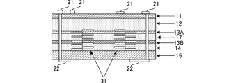
- FIG. 6 there may be a mode in which two intermediate layers of a nonmagnetic ferrite layer 13A and a nonmagnetic ferrite layer 13B are arranged, or a larger number of intermediate layers may be arranged.
- the thickness of one surface side of the outermost nonmagnetic ferrite layer is different from the thickness of the other surface side, and the inductor 31 is If the non-magnetic ferrite layer, which is an intermediate layer, is arranged so as to be biased to any surface side, the warpage of the entire element can be suppressed.
- the magnetic ferrite layer 17 is disposed on the lower surface side of the nonmagnetic ferrite layer 13A. Since the number of coil patterns is larger than the number of coil patterns arranged on the magnetic ferrite layer 12 on the upper surface side of the nonmagnetic ferrite layer 13A, either one is sandwiched between the nonmagnetic ferrite layers that are intermediate layers. It is the aspect arrange
- the nonmagnetic ferrite layer 13B, and the magnetic ferrite layer 14 are arranged on the magnetic ferrite layer 14 on the lower surface side of the nonmagnetic ferrite layer 13B.
- the number of coil patterns is larger than the number of coil patterns arranged on the magnetic ferrite layer 17 on the upper surface side of the nonmagnetic ferrite layer 13B. It is the aspect arrange
- the inductor is arranged in any direction on either side of the intermediate layer (non-magnetic ferrite layer) in the stacking direction, the warpage of the entire element can be suppressed. it can.
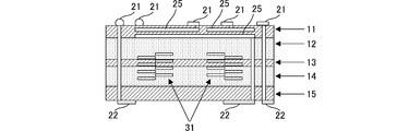
- an internal electrode 25 is formed in the nonmagnetic ferrite layer 11 and a capacitor is incorporated is also possible. That is, as shown in FIG. 7, a plurality of internal electrodes 25 are formed on each substrate of the nonmagnetic ferrite layer 11, and the plurality of internal electrodes 25 are arranged so as to face each other in the nonmagnetic ferrite layer 11. Then, a capacitor is formed by these opposed internal electrodes 25.
- FIG. 7 shows an example in which a capacitor is built in the element shown in FIG. 1A, but a capacitor is also built in the element shown in FIGS. 1B and 1C. In addition, it is possible to incorporate a capacitor in the element shown in FIG.
Landscapes
- Engineering & Computer Science (AREA)
- Power Engineering (AREA)
- Microelectronics & Electronic Packaging (AREA)
- Manufacturing & Machinery (AREA)
- Coils Or Transformers For Communication (AREA)
- Manufacturing Cores, Coils, And Magnets (AREA)
Abstract
積層型インダクタ素子は、上面側の非磁性体フェライト層(11)の厚みを薄くして素子全体としての低背化を実現しつつ、下面側の非磁性体フェライト層(15)の厚みを非磁性体フェライト層(11)よりも厚くして磁性体フェライト層(14)から拡散する金属成分が実装基板側のランド電極と電気的に接触する可能性を低くし、なおかつ、インダクタ(31)が非磁性体フェライト層(13)を挟んで下面側に偏って配置されるような構造とすることで、素子全体としての反りを抑える構成としている。
Description
この発明は、磁性体を含む複数の基板にコイルパターンが形成され、当該複数の基板が積層されてなる積層型インダクタ素子およびその製造方法に関するものである。
従来、複数の基板を積層した積層型素子が知られている。積層型素子では、各層の熱収縮率の違いにより、焼成によって素子全体に反りが生じるという課題点がある。
そこで、例えば特許文献1では、種類の異なる材料を交互に積層することにより平坦性を向上させた積層型素子が記載されている。
また、特許文献2では、実装面側の最外層に非常に薄い低誘電体層(ガラス)を配置することで反りを抑えることが記載されている。
しかし、磁性体にコイルパターンを形成して積層する積層型インダクタ素子においては、種類の異なる材料(例えば磁性体層と非磁性体層)を交互に積層することができない。また、最外層に磁性体層とは異なる材料からなる薄い層を配置すると、積層型インダクタ素子の端面において、コイルパターンを形成している金属成分が、磁性体に拡散し、実装基板との間で意図しない短絡が発生するおそれがあった。
そこで、この発明は、基板の平坦性を向上しつつも、磁性体からの拡散金属成分と実装基板との接触を防止し、意図しない短絡を防止する積層型インダクタ素子およびその製造方法を提供することを目的とする。
本発明の積層型インダクタ素子は、複数の磁性体基板が積層されてなる磁性体層と、複数の非磁性体基板が積層されてなる非磁性体層と、積層される基板間に設けられたコイルを、積層方向に接続したインダクタと、を備えている。そして、非磁性体層は、素子本体の最外層および中間層に配置され、最外層の非磁性体層は、一方の面側の厚さと、他方の面側の厚さとが異なり、インダクタは、積層方向において、中間層に設けられた非磁性体層を挟んで、いずれかの面側に偏って配置されていることを特徴とする。
このように、素子本体(積層体)の最外層の非磁性体層のうち、いずれか一方の面側の厚さが薄くなっていることで素子全体としての低背化を実現しつつ、他方の面側の厚さが厚くなっていることで、磁性体に拡散する金属成分が実装基板との間で、意図しない電気的接触を起こす可能性を低くし、短絡を防止することができる。また、インダクタは、中間層である非磁性体層を挟んでいずれかの面側に偏って配置されているため、熱収縮率の違いにより発生する反りを防止することができる。例えば、非磁性体層の熱収縮率が磁性体層の熱収縮率より低い場合において、非磁性体層の厚さが厚くなっている面側に、熱収縮率のより低いインダクタが偏って配置されていると、素子全体としての反りを抑えることができる。
また、本発明において、一方の面側に電子部品モジュールとしての電子部品が実装され、他方の面側に電子機器の実装基板側のランド電極等と接続するための端子電極が設けられる場合、一方の面側の非磁性体層の厚さが他方の面側の非磁性体層の厚さよりも薄いことが好ましい。
積層型インダクタ素子にICやコンデンサ等の電子部品を実装し、電子部品モジュールとする場合、これらICやコンデンサの実装を考慮して積層型インダクタ素子の上面に電極を配置するため、ICやコンデンサの電極が素子正面の電極をより大きくなることはなく、素子上面からはみ出すことはない。しかし、積層型インダクタ素子が電子部品モジュールとして出荷された後、電子機器の製品製造工程において、電子部品モジュールが実装される実装基板側のランド電極には様々な大きさのものが存在するため、電子部品モジュールの端子電極の大きさよりも、実装基板側のランド電極が大きくなる場合がある。この場合、実装基板側のランド電極に塗布されたはんだが濡れ上がり、積層型インダクタ素子の側面側に拡散した金属成分と実装基板側のランド電極とが電気的に接続され、意図しない短絡が発生する可能性がある。そこで、電子機器の実装基板と接続される端子電極が設けられる面側の厚みを厚くし、できるだけ拡散した金属成分と実装基板側のランド電極とが接触しないようにすることが好ましい。
なお、上記発明において、インダクタが積層方向において中間層に設けられた非磁性体層を挟んでいずれかの面側に偏って配置されるためには、例えば、インダクタが前記積層方向において、前記中間層に設けられた非磁性体層を挟んで、前記他方の面側に偏って配置されている態様が考えられる。また、中間層に設けられた非磁性体層が前記積層方向において、いずれかの面側に偏って配置されている態様も可能である。また、インダクタが前記積層方向において、前記中間層に設けられた非磁性体層を挟んで、前記他方の面側に偏って配置され、かつ中間層に設けられた非磁性体層が前記積層方向において、いずれかの面側に偏って配置されている態様も可能である。
また、上記発明において、最外層の非磁性体層のうち厚い側の非磁性体層の厚さは、ブレイク用溝の深さよりも厚いことが好ましい。ブレイク用溝の深さよりも非磁性体層の厚さが厚ければ、ブレイク前には磁性体層は表面に露出することがなく、焼成によって拡散した金属成分も表面に露出しない。
また、ブレイク用溝が、互いに直交する2方向に沿って設けられ、かつ、これら2方向で深さが異なる場合、厚い側の非磁性体層の厚さが、前記ブレイク用溝のうち、浅い方の溝の深さよりも厚くすればよい。
通常、めっき時には、ブレイク前のマザー積層体をある一定の方向に揺動させる。この揺動する方向と同じ方向に設けられた溝には、めっき液の滞留がないため、拡散した金属成分がめっき成長することがない。しかし、揺動する方向に直交する方向には、めっき液が滞留しやすいため、拡散した金属成分がめっき成長しやすい。そのため、非磁性体層の厚みは、揺動する方向に直交する方向の溝よりも厚ければよい。ここで、揺動する方向と同じ方向に設けられた溝を深く、直交する方向に設けられた溝を浅くすれば、非磁性体層の厚みをできるだけ薄くすることが可能となる。
なお、本発明の積層型インダクタ素子は、磁性体層として、鉄、ニッケル、亜鉛、および銅を含むフェライトを用い、非磁性体層は、鉄、亜鉛、および銅を含むフェライトを用い、インダクタは、銀材料を用いる例を示している。この場合、磁性体層の熱収縮率が非磁性体層の熱収縮率より高く、かつインダクタが最も低い熱収縮率となっているため、インダクタが非磁性体層を挟んで下面側に偏って配置する態様とすれば素子全体としての反りを抑えることができるが、材料の違い(熱収縮率の違い)によっては、逆にインダクタが非磁性体層を挟んで上面側に偏って配置する態様も考えられる。
この発明によれば、基板の平坦性を向上しつつも、磁性体からの拡散金属成分と実装基板との意図しない電気的接触を防止し、短絡を防止することができる。
図1(A)は、本発明の実施形態に係る積層型インダクタ素子の断面図である。積層型インダクタ素子は、磁性体および非磁性体のセラミックグリーンシートが積層されてなる。本実施形態に示す断面図は、紙面上側を積層型インダクタ素子の上面側とし、紙面下側を積層型インダクタ素子の下面側とする。
図1(A)の例における積層型インダクタ素子では、最外層のうち上面側から下面側に向かって順に、非磁性体フェライト層11、磁性体フェライト層12、非磁性体フェライト層13、磁性体フェライト層14、および非磁性体フェライト層15が配置された積層体からなる。
積層体を構成する一部のセラミックグリーンシート上には、コイルパターンを含む内部電極が形成されている。コイルパターンは、積層方向に接続され、インダクタ31を構成する。図1(A)の例におけるインダクタ31は、上面側の磁性体フェライト層12、中間層である非磁性体フェライト層13、および下面側の磁性体フェライト層14にわたって配置されている。
非磁性体フェライト層11の上面(素子最上面)には、外部電極21が形成されている。外部電極21は、ICやコンデンサ等が実装される。これにより、積層型インダクタ素子は、電子部品モジュール(例えばDC-DCコンバータ等)となる。
また、非磁性体フェライト層15の下面(素子最下面)には、端子電極22が形成される。この端子電極22は、積層型インダクタ素子が電子部品モジュールとして出荷された後、電子機器の製品製造工程において、電子部品モジュールが実装される、実装基板側のランド電極等と接続されるための端子電極となる。外部電極21と端子電極22は、貫通ビアで電気的に接続される。
中間層である非磁性体フェライト層13は、磁性体フェライト層12および磁性体フェライト層14間の空隙として機能し、インダクタ31の直流重畳特性を向上させるものである。図1(A)の例における非磁性体フェライト層13は、積層方向において、積層型インダクタ素子の中央に配置されている。
最外層である非磁性体フェライト層11および非磁性体フェライト層15は、磁性体フェライト層12および磁性体フェライト層14の上面側および下面側をそれぞれ被覆し、後述する拡散金属成分による、意図しない短絡を防止するものである。
また、本実施形態における非磁性体フェライト層11および非磁性体フェライト層15は、磁性体フェライト層12および磁性体フェライト層14よりも熱収縮率が低くなっている。そのため、相対的に熱収縮率の高い磁性体フェライト層12および磁性体フェライト層14を、相対的に熱収縮率の低い非磁性体フェライト層11および非磁性体フェライト層15で挟みこむことで、焼成により素子全体を圧縮して強度を向上させることができる。
ただし、熱収縮率の違う材料を積層して焼成すると、積層方向に応力が生じて素子全体として反りが生じるおそれがある。従来は、図2に例示するように、積層方向の中央に非磁性体フェライト層を配置し、積層方向において対称に磁性体フェライト層および非磁性体フェライト層を配置することで素子全体としての応力のバランスをとり、反りを抑えていた。しかし、図2に示すように、素子全体として低背化を実現するために最外層の非磁性体フェライト層を薄くすると、焼成時に金属成分90が磁性体フェライト層12および磁性体フェライト層14から拡散し、めっき時にこの拡散した金属成分が成長して、実装基板側のランド電極71とはんだを介して接触することで意図しない短絡が発生する可能性がある。特に、ICやコンデンサ等の出荷前に実装する電子部品については、これら電子部品の実装を考慮して積層型インダクタ素子の上面電極を形成するため、ICやコンデンサ等の電極70の面積が外部電極21の面積より大きくなることはなく、電極70が素子上面からはみ出すことはない。しかし、積層型インダクタ素子が電子部品モジュールとして出荷された後、電子機器の製品製造工程において実装基板側のランド電極には、様々な大きさのものがあり、当該実装基板側のランド電極71は、端子電極22よりも面積が大きくなる場合がある。この場合、ランド電極71上のはんだが濡れ上がり、積層型インダクタ素子の側面側に拡散した金属成分90と電気的に接触し、意図しない短絡が生じる可能性が高くなる。
そこで、本実施形態の積層型インダクタ素子は、上面側の非磁性体フェライト層11の厚みを薄くして素子全体としての低背化を実現しつつ、下面側の非磁性体フェライト層15の厚みを非磁性体フェライト層11よりも厚くして磁性体フェライト層14から拡散する金属成分が実装基板側のランド電極と接触する可能性を低くし、なおかつ、インダクタ31が非磁性体フェライト層13を挟んで下面側に偏って配置されるような構造とすることで、素子全体としての反りを抑える構成としている。
各層の厚みを変更するには、例えば積層するセラミックグリーンシートの枚数を変更する、あるいはセラミックグリーンシート自体の厚みが異なるものを用いる。
なお、本実施形態では、磁性体フェライト層として、鉄、ニッケル、亜鉛、および銅を含むフェライトを用い、非磁性体フェライト層として、鉄、亜鉛、および銅を含むフェライトを用い、インダクタ31を含む内部配線として銀材料を用いる例を示している。この場合、磁性体フェライト層の熱収縮率が非磁性体フェライト層の熱収縮率より高く、かつインダクタ31が最も低い熱収縮率となっているため、インダクタ31が非磁性体フェライト層13を挟んで下面側に偏って配置する態様とすれば素子全体としての反りを抑えることができるが、材料の違い(熱収縮率の違い)によっては、逆にインダクタ31が非磁性体フェライト層13を挟んで上面側に偏って配置する態様も考えられる。いずれにしても、最外層の非磁性体フェライト層の一方の面側の厚さと他方の面側の厚さとが異なり、インダクタ31が積層方向において、非磁性体フェライト層13を挟んでいずれかの面側に偏って配置されている態様であれば、素子全体としての反りを抑えることができる。
ここで、インダクタ31が非磁性体フェライト層13を挟んで下面側に偏って配置されるためには、例えば、図1(A)に示すように、非磁性体フェライト層13が中央に配置され、インダクタ31が下面側に偏って配置されている態様とする。この場合、インダクタ31は、非磁性体フェライト層13を挟んで相対的に下面側に偏って配置されることになり、素子全体としての反りを抑えることができる。
一方、図1(B)に示す積層型インダクタ素子は、図1(A)に示した積層型インダクタ素子と同様の構成であるが、インダクタ31が積層方向において対称に配置され、非磁性体フェライト層13が上面側に偏って配置されている態様である。この場合も、インダクタ31は、非磁性体フェライト層13を挟んで相対的に下面側に偏って配置されることになり、素子全体としての反りを抑えることができる。
また、図3(C)に示す積層型インダクタ素子についても、図1(A)に示した積層型インダクタ素子と同様の構成であるが、インダクタ31が下面側に偏って配置され、かつ非磁性体フェライト層13も上面側に偏って配置されている態様である。この場合も、インダクタ31は、非磁性体フェライト層13を挟んで相対的に下面側に偏って配置されることになり、素子全体としての反りを抑えることができる。
次に、ブレイク前の積層型インダクタ素子について説明する。図3は、ブレイク前の積層型インダクタ素子(マザー積層体)の断面図である。なお、同図においては、説明のために隣接する2つのチップについてブレイク前の断面図を示すが、実際にはさらに多数のチップが並んでいる。
図3に示すように、ブレイク前のマザー積層体は、出荷先で所定寸法のチップにブレイク可能となるように、ダイシング加工により上面および下面に溝51が形成されている。溝51は、上面側がV字溝、下面側が矩形溝となっており、V字溝を外側に、矩形溝を内側にして曲げることでマザー積層体を各チップにブレイクすることができる。
ここで、最外層の非磁性体フェライト層のうち厚い側の非磁性体フェライト層15の厚さは、ブレイク用の溝51の深さよりも厚くなっている。このように、ブレイク用の溝51の深さよりも非磁性体フェライト層15層の厚さが厚ければ、下面側に磁性体フェライト層14が露出することがなく、金属成分が拡散することがない。
さらに、図4の下面図に示すように、ブレイク用の溝は、互いに直交する2方向に沿って設けられている。すなわち、めっき時にマザー積層体を揺動させる方向と同じ方向の溝51Aと、揺動する方向に直交する方向の溝51Bが設けられている。
溝51Aは、めっき時の揺動方向と同じ方向に設けられているため、揺動によりめっき液が溝から外れ、滞留することがないため、拡散した金属成分がめっき成長しにくい。しかし、溝51Bは、めっき液が滞留しやすいため、拡散した金属成分がめっき成長しやすい。
そこで、図5(A)のA-A断面図、および図5(B)のB-B断面図に示すように、揺動方向と同じ方向に設けられた溝51Aを深く、直交する方向に設けられた溝51Bを浅くする。溝51Aには、めっき液が滞留することがないため、溝51Aの深さより非磁性体フェライト層15の厚みが薄く、磁性体フェライト層14が露出したとしても拡散した金属成分はめっき成長しにくい。したがって、図5(B)に示すように、非磁性体フェライト層15の厚みは、溝51Bよりも厚ければよい。これにより、非磁性体フェライト層15の厚みをできるだけ薄くすることが可能となる。
次に、積層型インダクタ素子の製造工程について説明する。積層型インダクタ素子は、以下の工程により製造される。
まず、磁性体フェライト層及び非磁性体層フェライト層となるべきセラミックグリーンシート上に、それぞれAg等が含まれる合金(導電性ペースト)が塗布され、コイルパターン等の内部電極が形成される。
次に、各セラミックグリーンシートが積層される。すなわち、下面側から順に、非磁性体フェライト層15となるべきセラミックグリーンシートが複数枚、磁性体フェライト層14となるべきセラミックグリーンシートが複数枚、非磁性体フェライト層13となるべきセラミックグリーンシートが複数枚、磁性体フェライト層12となるべきセラミックグリーンシートが複数枚、および非磁性体フェライト層11となるべきセラミックグリーンシートが複数枚、それぞれ積層され、仮圧着を行われる。これにより、焼成前のマザー積層体が形成される。
このとき、各セラミックグリーンシートの枚数、またはシート毎の厚みを調整することにより、各層の厚みが調整される。非磁性体フェライト層15となるべきセラミックグリーンシートは、枚数が多く配置される、または厚いものが用いられる。また、非磁性体フェライト層11となるべきセラミックグリーンシートは、枚数が少なく配置される、または薄いものが用いられる。
ここで、非磁性体フェライト層15は、ブレイク用の溝の深さよりも厚くなるように調整される。特に、ブレイク用の溝は、後述の溝形成工程において、互いに直交する2方向に沿って設けられ、深さが異なるものとなっている。そこで、非磁性体フェライト層15の厚みは、浅い方のブレイク用の溝よりも厚くなるように調整される。
そして、図1(A)に示した構造の積層型インダクタ素子を製造する場合、コイルパターンを形成したセラミックグリーンシートが下面側に偏って配置される。これにより、素子全体としての低背化を実現しつつ、磁性体フェライト層14から拡散する金属成分が実装基板側のランド電極と接触する可能性を低くし、なおかつ、素子全体としての反りを抑えることができる。
また、図1(B)に示した構造の積層型インダクタ素子を製造する場合、コイルパターンを形成したセラミックグリーンシートが積層方向に対称に配置され、非磁性体フェライト層13となるべきセラミックグリーンシートが上面側に偏って配置される。図1(C)に示した構造の積層型インダクタ素子を製造する場合、コイルパターンを形成したセラミックグリーンシートが下面側に偏って配置され、かつ非磁性体フェライト層13となるべきセラミックグリーンシートが上面側に偏って配置される。
次に、形成したマザー積層体の表面には、主成分が銀である電極ペーストが塗布され、外部電極21および端子電極22が形成される。
その後、マザー積層体を所定の寸法でブレイク可能となるように、ダイシング加工によりブレイク用の溝が設けられる。ブレイク用の溝は、図4および図5に示したように、互いに直交する2方向に沿って設けられる。このとき、一方の溝の深さと、他方の溝の深さを異なるものとされる。これは、マザー積層体の最初のブレイク時に深い溝でブレイクを行うことで、意図しない方向に割れが生じないようにするためである。
次に、焼成がなされる。これにより、焼成されたマザー積層体(ブレイク前の積層型インダクタ素子)が得られる。
そして、最後にマザー積層体の外部電極表面にめっきが施される。めっき処理は、マザー積層体をめっき液に浸漬させ、揺動させることによって行われる。このとき、深い溝が形成された方向にマザー積層体を揺動させる。図5(A)に示したように、非磁性体フェライト層15の厚みは、浅い方の溝よりも厚くなるように調整され、深い方の溝よりも薄くなっている場合もあるが、深い方の溝が形成された方向とマザー積層体の揺動方向とを一致させることで、めっき液が溝に滞留することがなくなり、拡散した金属成分がめっき成長することがなくなる。このようにして製造された積層型インダクタ素子は、ICやコンデンサ等の電子部品を実装すれば、電子部品モジュールとなる。
なお、本実施形態では、中間層が非磁性体フェライト層13の1つである例を示したが、中間層は1つである必要はない。例えば図6に示すように、非磁性体フェライト層13Aおよび非磁性体フェライト層13Bの2つの中間層を配置する態様も可能であるし、さらに多数の中間層を配置することも可能である。
図6のように複数の中間層を設ける場合であっても、最外層の非磁性体フェライト層の一方の面側の厚さと他方の面側の厚さとが異なり、インダクタ31が積層方向において、中間層である非磁性体フェライト層を挟んでいずれかの面側に偏って配置されている態様であれば、素子全体としての反りを抑えることができる。
例えば、上面側から順に磁性体フェライト層12、非磁性体フェライト層13、および磁性体フェライト層17を参照した場合、非磁性体フェライト層13Aの下面側の磁性体フェライト層17に配置されているコイルパターンは、非磁性体フェライト層13Aの上面側の磁性体フェライト層12に配置されているコイルパターンよりも数が多くなっているため、中間層である非磁性体フェライト層を挟んでいずれかの面側に偏って配置されている態様となっている。同様に、上面側から順に磁性体フェライト層17、非磁性体フェライト層13B、および磁性体フェライト層14を参照した場合、非磁性体フェライト層13Bの下面側の磁性体フェライト層14に配置されているコイルパターンは、非磁性体フェライト層13Bの上面側の磁性体フェライト層17に配置されているコイルパターンよりも数が多くなっているため、中間層である非磁性体フェライト層を挟んでいずれかの面側に偏って配置されている態様となっている。
このように、インダクタが積層方向において、それぞれの中間層(非磁性体フェライト層)を挟んでいずれかの面側に偏って配置されている態様であれば、素子全体としての反りを抑えることができる。
無論、複数の中間層を配置する場合においても、各層の熱収縮率の違いによっては、インダクタが下面側に偏って配置される場合と、逆に上面側に偏って配置される場合とが考えられる。
なお、本実施形態の積層型インダクタ素子では、図7に示すように、非磁性フェライト層11内に内部電極25を形成し、コンデンサを内蔵させる応用例も可能である。すなわち、図7に示すように、非磁性体フェライト層11の各基板上に複数の内部電極25を形成し、これら複数の内部電極25が非磁性体フェライト層11内で対向するように配置されると、これらの対向した内部電極25によってコンデンサが形成されることになる。
図7では、図1(A)に示した態様の素子において、コンデンサを内蔵させる例を示したが、図1(B)や図1(C)に示した態様の素子においてもコンデンサを内蔵させることも可能であるし、図6に示した態様の素子においてもコンデンサを内蔵させることは可能である。
11,13,15…非磁性体フェライト層
12,14…磁性体フェライト層
21…外部電極
22…端子電極
31…インダクタ
12,14…磁性体フェライト層
21…外部電極
22…端子電極
31…インダクタ
Claims (15)
- 複数の磁性体基板が積層されてなる磁性体層と、
複数の非磁性体基板が積層されてなる非磁性体層と、
前記積層される基板間に設けられたコイルを、積層方向に接続したインダクタと、
を備えた積層型インダクタ素子であって、
前記非磁性体層は、素子本体の最外層および中間層に配置され、
前記最外層の非磁性体層は、一方の面側の厚さと、他方の面側の厚さとが異なり、
前記インダクタは、前記積層方向において、前記中間層に設けられた非磁性体層を挟んで、いずれかの面側に偏って配置されていることを特徴とする積層型インダクタ素子。 - 前記一方の面側は、電子部品モジュールとしての電子部品が実装され、前記他方の面側は、該電子部品モジュールが実装される実装基板のランド電極と接続される端子電極が設けられ、
前記一方の面側の非磁性体層の厚さは、前記他方の面側の非磁性体層の厚さよりも薄いことを特徴とする請求項1に記載の積層型インダクタ素子。 - 前記複数の非磁性体基板上に内部電極を有し、前記非磁性体層内でコンデンサが形成されていることを特徴とする請求項1または2に記載の積層型インダクタ素子。
- 前記インダクタは、前記積層方向において、前記中間層に設けられた非磁性体層を挟んで、前記他方の面側に偏って配置されていることを特徴とする請求項1ないし請求項3のいずれかに記載の積層型インダクタ素子。
- 前記中間層に設けられた非磁性体層は、前記積層方向において、いずれかの面側に偏って配置されていることを特徴とする請求項1ないし請求項4のいずれかに記載の積層型インダクタ素子。
- 前記最外層の非磁性体層のうち厚い側の非磁性体層の厚さは、ブレイク用溝の深さよりも厚いことを特徴とする請求項1ないし請求項5のいずれかに記載の積層型インダクタ素子。
- 前記ブレイク用溝は、互いに直交する2方向に沿って設けられ、かつ、これら2方向で深さが異なり、
前記厚い側の非磁性体層の厚さは、前記ブレイク用溝のうち、浅い方の溝の深さよりも厚いことを特徴とする請求項6に記載の積層型インダクタ素子。 - 前記磁性体は、鉄、ニッケル、亜鉛、および銅を含むフェライトであり、前記非磁性体は、鉄、亜鉛、および銅を含むフェライトであり、前記インダクタは、銀材料であることを特徴とする請求項1ないし請求項7のいずれかに記載の積層型インダクタ素子。
- 磁性体基板を含む複数の基板にコイルパターンを形成する工程と、
前記基板を積層して積層体を形成するとともに、前記コイルパターンを積層方向に接続してインダクタを形成する工程と、
を有する積層型インダクタ素子の製造方法であって、
前記基板を積層する工程において、前記積層体の最外層および中間層に、非磁性体基板を積層してなる非磁性体層を配置し、
前記最外層の非磁性体層の一方の面側の厚さと、他方の面側の厚さとが異なるように前記積層体を形成し、
前記インダクタを、前記積層方向において、前記中間層に設けられた非磁性体層を挟んで、いずれかの面側に偏って配置することを特徴とする積層型インダクタ素子の製造方法。 - 前記一方の面側に、電子部品モジュールとしての電子部品を実装するための電極を設ける工程と、
前記他方の面側に、該電子部品モジュールが実装される実装基板のランド電極と接続される端子電極を設ける工程と、
を有し、
前記一方の面側の非磁性体層の厚さを、前記他方の面側の非磁性体層の厚さよりも薄くすることを特徴とする請求項9に記載の積層型インダクタ素子の製造方法。 - 前記複数の非磁性体基板上に内部電極を形成する工程をさらに有し、
前記内部電極により前記非磁性体層内でコンデンサを形成することを特徴とする請求項9または10に記載の積層型インダクタ素子の製造方法。 - 前記インダクタを、前記積層方向において、前記中間層に設けられた非磁性体層を挟んで、前記他方の面側に偏って配置することを特徴とする請求項9ないし請求項11のいずれかに記載の積層型インダクタ素子の製造方法。
- 前記中間層に設けられた非磁性体層を、前記積層方向において、いずれかの面側に偏って配置することを特徴とする請求項9ないし請求項12のいずれかに記載の積層型インダクタ素子の製造方法。
- 前記基板を積層する工程の後、前記一方の面側、および他方の面側にブレイク用溝を形成する工程を有し、
前記基板を積層する工程において、前記最外層の非磁性体層のうち薄い側の非磁性体層の厚さを、前記ブレイク用溝の深さよりも厚くすることを特徴とする請求項9ないし請求項13のいずれかに記載の積層型インダクタ素子の製造方法。 - 前記ブレイク用溝を形成する工程の後、前記積層体を揺動させて外部電極をめっきする工程を有し、
前記ブレイク用溝を形成する工程において、前記ブレイク用溝を、互いに直交する2方向に沿って、かつ、これら2方向で深さが異なるように設け、
前記基板を積層する工程において、前記厚い側の非磁性体層の厚さを、前記ブレイク用溝のうち、浅い方の溝の深さよりも厚くし、
前記外部電極をめっきする工程において、前記ブレイク用溝のうち、深いほうの溝を前記積層体の揺動方向に一致させることを特徴とする請求項14に記載の積層型インダクタ素子の製造方法。
Priority Applications (4)
| Application Number | Priority Date | Filing Date | Title |
|---|---|---|---|
| EP11862903.9A EP2696357B1 (en) | 2011-04-06 | 2011-11-24 | Laminated-type inductor element and method of manufacturing thereof |
| JP2012531138A JP5510554B2 (ja) | 2011-04-06 | 2011-11-24 | 積層型インダクタ素子およびその製造方法 |
| CN201180069322.6A CN103430252B (zh) | 2011-04-06 | 2011-11-24 | 层叠型电感元件及其制造方法 |
| US13/955,488 US9129733B2 (en) | 2011-04-06 | 2013-07-31 | Laminated inductor element and manufacturing method thereof |
Applications Claiming Priority (2)
| Application Number | Priority Date | Filing Date | Title |
|---|---|---|---|
| JP2011084212 | 2011-04-06 | ||
| JP2011-084212 | 2011-04-06 |
Related Child Applications (1)
| Application Number | Title | Priority Date | Filing Date |
|---|---|---|---|
| US13/955,488 Continuation US9129733B2 (en) | 2011-04-06 | 2013-07-31 | Laminated inductor element and manufacturing method thereof |
Publications (1)
| Publication Number | Publication Date |
|---|---|
| WO2012137386A1 true WO2012137386A1 (ja) | 2012-10-11 |
Family
ID=46968808
Family Applications (1)
| Application Number | Title | Priority Date | Filing Date |
|---|---|---|---|
| PCT/JP2011/076986 Ceased WO2012137386A1 (ja) | 2011-04-06 | 2011-11-24 | 積層型インダクタ素子およびその製造方法 |
Country Status (5)
| Country | Link |
|---|---|
| US (1) | US9129733B2 (ja) |
| EP (1) | EP2696357B1 (ja) |
| JP (1) | JP5510554B2 (ja) |
| CN (1) | CN103430252B (ja) |
| WO (1) | WO2012137386A1 (ja) |
Cited By (4)
| Publication number | Priority date | Publication date | Assignee | Title |
|---|---|---|---|---|
| WO2013175655A1 (ja) * | 2012-05-21 | 2013-11-28 | 株式会社村田製作所 | 積層型素子およびその製造方法 |
| US10332674B2 (en) | 2016-04-19 | 2019-06-25 | Murata Manufacturing Co., Ltd. | Electronic component |
| JP2019180021A (ja) * | 2018-03-30 | 2019-10-17 | 戸田工業株式会社 | モジュール基板用アンテナ、及びそれを用いたモジュール基板 |
| JP2020061410A (ja) * | 2018-10-05 | 2020-04-16 | 株式会社村田製作所 | 積層型電子部品 |
Families Citing this family (15)
| Publication number | Priority date | Publication date | Assignee | Title |
|---|---|---|---|---|
| US9406438B2 (en) * | 2013-03-18 | 2016-08-02 | Murata Manufacturing Co., Ltd. | Stack-type inductor element and method of manufacturing the same |
| CN105849831B (zh) * | 2014-06-04 | 2018-01-19 | 株式会社村田制作所 | 电子部件及其制造方法 |
| JP6376000B2 (ja) * | 2015-03-02 | 2018-08-22 | 株式会社村田製作所 | 電子部品およびその製造方法 |
| KR102217286B1 (ko) * | 2015-04-01 | 2021-02-19 | 삼성전기주식회사 | 하이브리드 인덕터 및 그 제조방법 |
| DE102015206173A1 (de) | 2015-04-07 | 2016-10-13 | Würth Elektronik eiSos Gmbh & Co. KG | Elektronisches Bauteil und Verfahren zum Herstellen eines elektronischen Bauteils |
| TWI623247B (zh) * | 2015-06-25 | 2018-05-01 | 威華微機電股份有限公司 | Mass production method of preform of passive component |
| TWI629694B (zh) * | 2015-06-25 | 2018-07-11 | 威華微機電股份有限公司 | Mass production method of preform of magnetic core inductor |
| JP6648689B2 (ja) * | 2016-12-28 | 2020-02-14 | 株式会社村田製作所 | 積層型電子部品の製造方法および積層型電子部品 |
| JP6729422B2 (ja) * | 2017-01-27 | 2020-07-22 | 株式会社村田製作所 | 積層型電子部品 |
| KR101863280B1 (ko) * | 2017-03-16 | 2018-05-31 | 삼성전기주식회사 | 코일부품 및 그 제조방법 |
| US11239019B2 (en) | 2017-03-23 | 2022-02-01 | Tdk Corporation | Coil component and method of manufacturing coil component |
| JP6828555B2 (ja) | 2017-03-29 | 2021-02-10 | Tdk株式会社 | コイル部品およびその製造方法 |
| JP6919641B2 (ja) | 2018-10-05 | 2021-08-18 | 株式会社村田製作所 | 積層型電子部品 |
| JP7247818B2 (ja) * | 2019-08-29 | 2023-03-29 | 株式会社村田製作所 | 積層型インダクタ |
| JP7099434B2 (ja) * | 2019-11-29 | 2022-07-12 | 株式会社村田製作所 | コイル部品 |
Citations (8)
| Publication number | Priority date | Publication date | Assignee | Title |
|---|---|---|---|---|
| JPH0786754A (ja) * | 1993-09-16 | 1995-03-31 | Tdk Corp | 積層型混成集積回路部品 |
| JPH10270813A (ja) * | 1997-03-27 | 1998-10-09 | Murata Mfg Co Ltd | ブレーク溝付きセラミック基板およびこのセラミック基板から製造される電子部品 |
| JP2004235374A (ja) | 2003-01-29 | 2004-08-19 | Kyocera Corp | コンデンサ内蔵基板及びチップ状コンデンサ |
| JP2005175159A (ja) * | 2003-12-10 | 2005-06-30 | Sumida Corporation | インダクタ |
| JP2005183890A (ja) * | 2003-12-24 | 2005-07-07 | Taiyo Yuden Co Ltd | 積層基板、複数種類の積層基板の設計方法、及び同時焼結積層基板 |
| WO2007145189A1 (ja) * | 2006-06-14 | 2007-12-21 | Murata Manufacturing Co., Ltd. | 積層型セラミック電子部品 |
| JP2008109063A (ja) * | 2006-09-27 | 2008-05-08 | Kyocera Corp | セラミック多層基板 |
| JP2009152489A (ja) | 2007-12-21 | 2009-07-09 | Ngk Spark Plug Co Ltd | セラミック多層部品 |
Family Cites Families (21)
| Publication number | Priority date | Publication date | Assignee | Title |
|---|---|---|---|---|
| JPS56155516A (en) | 1980-05-06 | 1981-12-01 | Tdk Corp | Laminated coil of open magnetic circuit type |
| JPH06232005A (ja) * | 1993-02-01 | 1994-08-19 | Tdk Corp | Lc複合部品 |
| JP2000252131A (ja) | 1999-03-01 | 2000-09-14 | Tdk Corp | 積層チップ部品 |
| JP3687484B2 (ja) * | 1999-06-16 | 2005-08-24 | 株式会社村田製作所 | セラミック基板の製造方法および未焼成セラミック基板 |
| JP3621300B2 (ja) * | 1999-08-03 | 2005-02-16 | 太陽誘電株式会社 | 電源回路用積層インダクタ |
| JP2001044037A (ja) * | 1999-08-03 | 2001-02-16 | Taiyo Yuden Co Ltd | 積層インダクタ |
| JP2001155938A (ja) * | 1999-09-17 | 2001-06-08 | Fdk Corp | 積層インダクタおよびその製造方法 |
| US6864774B2 (en) * | 2000-10-19 | 2005-03-08 | Matsushita Electric Industrial Co., Ltd. | Inductance component and method of manufacturing the same |
| JP3724405B2 (ja) * | 2001-10-23 | 2005-12-07 | 株式会社村田製作所 | コモンモードチョークコイル |
| JP2003238259A (ja) * | 2002-02-21 | 2003-08-27 | Matsushita Electric Ind Co Ltd | セラミック部品の製造方法 |
| WO2004100187A1 (ja) * | 2003-05-08 | 2004-11-18 | Matsushita Electric Industrial Co., Ltd. | 電子部品及びその製造方法 |
| JP2005045103A (ja) * | 2003-07-24 | 2005-02-17 | Tdk Corp | チップインダクタ |
| WO2005122192A1 (ja) * | 2004-06-07 | 2005-12-22 | Murata Manufacturing Co., Ltd. | 積層コイル |
| JP2007266105A (ja) * | 2006-03-27 | 2007-10-11 | Tdk Corp | 薄膜デバイス |
| KR101174541B1 (ko) * | 2007-02-02 | 2012-08-16 | 가부시키가이샤 무라타 세이사쿠쇼 | 적층 코일 부품 |
| JP4674590B2 (ja) * | 2007-02-15 | 2011-04-20 | ソニー株式会社 | バラントランス及びバラントランスの実装構造、並びに、この実装構造を内蔵した電子機器 |
| JP5024064B2 (ja) | 2008-01-15 | 2012-09-12 | 株式会社村田製作所 | 多層セラミック基板およびその製造方法 |
| JP2011071457A (ja) * | 2008-12-22 | 2011-04-07 | Tdk Corp | 電子部品及び電子部品の製造方法 |
| US8243960B2 (en) * | 2010-03-04 | 2012-08-14 | Bose Corporation | Planar audio amplifier output inductor with current sense |
| JP5196038B2 (ja) * | 2010-07-16 | 2013-05-15 | 株式会社村田製作所 | コイル内蔵基板 |
| CN103443879B (zh) * | 2011-04-11 | 2016-01-20 | 株式会社村田制作所 | 层叠型电感元件及其制造方法 |
-
2011
- 2011-11-24 WO PCT/JP2011/076986 patent/WO2012137386A1/ja not_active Ceased
- 2011-11-24 EP EP11862903.9A patent/EP2696357B1/en active Active
- 2011-11-24 JP JP2012531138A patent/JP5510554B2/ja active Active
- 2011-11-24 CN CN201180069322.6A patent/CN103430252B/zh active Active
-
2013
- 2013-07-31 US US13/955,488 patent/US9129733B2/en active Active
Patent Citations (8)
| Publication number | Priority date | Publication date | Assignee | Title |
|---|---|---|---|---|
| JPH0786754A (ja) * | 1993-09-16 | 1995-03-31 | Tdk Corp | 積層型混成集積回路部品 |
| JPH10270813A (ja) * | 1997-03-27 | 1998-10-09 | Murata Mfg Co Ltd | ブレーク溝付きセラミック基板およびこのセラミック基板から製造される電子部品 |
| JP2004235374A (ja) | 2003-01-29 | 2004-08-19 | Kyocera Corp | コンデンサ内蔵基板及びチップ状コンデンサ |
| JP2005175159A (ja) * | 2003-12-10 | 2005-06-30 | Sumida Corporation | インダクタ |
| JP2005183890A (ja) * | 2003-12-24 | 2005-07-07 | Taiyo Yuden Co Ltd | 積層基板、複数種類の積層基板の設計方法、及び同時焼結積層基板 |
| WO2007145189A1 (ja) * | 2006-06-14 | 2007-12-21 | Murata Manufacturing Co., Ltd. | 積層型セラミック電子部品 |
| JP2008109063A (ja) * | 2006-09-27 | 2008-05-08 | Kyocera Corp | セラミック多層基板 |
| JP2009152489A (ja) | 2007-12-21 | 2009-07-09 | Ngk Spark Plug Co Ltd | セラミック多層部品 |
Cited By (6)
| Publication number | Priority date | Publication date | Assignee | Title |
|---|---|---|---|---|
| WO2013175655A1 (ja) * | 2012-05-21 | 2013-11-28 | 株式会社村田製作所 | 積層型素子およびその製造方法 |
| US9466416B2 (en) | 2012-05-21 | 2016-10-11 | Murata Manufacturing Co., Ltd. | Multilayer device and manufacturing method of the same |
| US10332674B2 (en) | 2016-04-19 | 2019-06-25 | Murata Manufacturing Co., Ltd. | Electronic component |
| JP2019180021A (ja) * | 2018-03-30 | 2019-10-17 | 戸田工業株式会社 | モジュール基板用アンテナ、及びそれを用いたモジュール基板 |
| JP7109232B2 (ja) | 2018-03-30 | 2022-07-29 | 戸田工業株式会社 | モジュール基板用アンテナ、及びそれを用いたモジュール基板 |
| JP2020061410A (ja) * | 2018-10-05 | 2020-04-16 | 株式会社村田製作所 | 積層型電子部品 |
Also Published As
| Publication number | Publication date |
|---|---|
| US20130314194A1 (en) | 2013-11-28 |
| JP5510554B2 (ja) | 2014-06-04 |
| EP2696357B1 (en) | 2019-02-06 |
| CN103430252B (zh) | 2017-03-29 |
| US9129733B2 (en) | 2015-09-08 |
| JPWO2012137386A1 (ja) | 2014-07-28 |
| CN103430252A (zh) | 2013-12-04 |
| EP2696357A4 (en) | 2014-09-24 |
| EP2696357A1 (en) | 2014-02-12 |
Similar Documents
| Publication | Publication Date | Title |
|---|---|---|
| JP5510554B2 (ja) | 積層型インダクタ素子およびその製造方法 | |
| JP5921074B2 (ja) | 積層基板の製造方法 | |
| US9478334B2 (en) | Magnetic module for power inductor, power inductor, and manufacturing method thereof | |
| JP6520433B2 (ja) | 積層コイル部品 | |
| KR20150014390A (ko) | 적층 코일 | |
| JP5621573B2 (ja) | コイル内蔵基板 | |
| JP2015050452A (ja) | 基板内蔵用積層セラミック電子部品及び積層セラミック電子部品内蔵型印刷回路基板 | |
| WO2012002133A1 (ja) | 積層型セラミック電子部品およびその製造方法 | |
| JP2022156320A (ja) | 積層電子部品 | |
| WO2012144103A1 (ja) | 積層型インダクタ素子及び製造方法 | |
| JP5831633B2 (ja) | 積層型素子およびその製造方法 | |
| JP2001251024A (ja) | 多層集合基板および多層セラミック部品の製造方法 | |
| JP7590904B2 (ja) | 積層電子部品 | |
| CN203760245U (zh) | 电感元件 | |
| WO2011148678A1 (ja) | Lc共焼結基板及びその製造方法 | |
| US6551426B2 (en) | Manufacturing method for a laminated ceramic electronic component | |
| JP2002305123A (ja) | 積層セラミック電子部品の製造方法及び積層インダクタの製造方法 | |
| JP2007305830A (ja) | 電子部品の製造方法、電子部品、及び電子機器 | |
| JP2010268261A (ja) | コモンモードノイズフィルタの製造方法 | |
| JP2006222441A (ja) | コンデンサ、配線基板、デカップリング回路及び高周波回路 | |
| JP2012151243A (ja) | 多層セラミック基板 | |
| JP2012109355A (ja) | 多層フェライト基板及び電子部品の製造方法 | |
| WO2014030471A1 (ja) | 積層基板およびその製造方法 | |
| CN119724825A (zh) | 层叠线圈部件 | |
| JP5119837B2 (ja) | コモンモードノイズフィルタ |
Legal Events
| Date | Code | Title | Description |
|---|---|---|---|
| ENP | Entry into the national phase |
Ref document number: 2012531138 Country of ref document: JP Kind code of ref document: A |
|
| 121 | Ep: the epo has been informed by wipo that ep was designated in this application |
Ref document number: 11862903 Country of ref document: EP Kind code of ref document: A1 |
|
| WWE | Wipo information: entry into national phase |
Ref document number: 2011862903 Country of ref document: EP |
|
| NENP | Non-entry into the national phase |
Ref country code: DE |