WO2012137659A1 - 半導体装置およびその製造方法 - Google Patents
半導体装置およびその製造方法 Download PDFInfo
- Publication number
- WO2012137659A1 WO2012137659A1 PCT/JP2012/058375 JP2012058375W WO2012137659A1 WO 2012137659 A1 WO2012137659 A1 WO 2012137659A1 JP 2012058375 W JP2012058375 W JP 2012058375W WO 2012137659 A1 WO2012137659 A1 WO 2012137659A1
- Authority
- WO
- WIPO (PCT)
- Prior art keywords
- conductivity type
- region
- jte
- thickness direction
- silicon carbide
- Prior art date
- Legal status (The legal status is an assumption and is not a legal conclusion. Google has not performed a legal analysis and makes no representation as to the accuracy of the status listed.)
- Ceased
Links
Images













Classifications
-
- H—ELECTRICITY
- H10—SEMICONDUCTOR DEVICES; ELECTRIC SOLID-STATE DEVICES NOT OTHERWISE PROVIDED FOR
- H10D—INORGANIC ELECTRIC SEMICONDUCTOR DEVICES
- H10D62/00—Semiconductor bodies, or regions thereof, of devices having potential barriers
- H10D62/80—Semiconductor bodies, or regions thereof, of devices having potential barriers characterised by the materials
- H10D62/83—Semiconductor bodies, or regions thereof, of devices having potential barriers characterised by the materials being Group IV materials, e.g. B-doped Si or undoped Ge
- H10D62/832—Semiconductor bodies, or regions thereof, of devices having potential barriers characterised by the materials being Group IV materials, e.g. B-doped Si or undoped Ge being Group IV materials comprising two or more elements, e.g. SiGe
- H10D62/8325—Silicon carbide
-
- H—ELECTRICITY
- H10—SEMICONDUCTOR DEVICES; ELECTRIC SOLID-STATE DEVICES NOT OTHERWISE PROVIDED FOR
- H10D—INORGANIC ELECTRIC SEMICONDUCTOR DEVICES
- H10D62/00—Semiconductor bodies, or regions thereof, of devices having potential barriers
- H10D62/10—Shapes, relative sizes or dispositions of the regions of the semiconductor bodies; Shapes of the semiconductor bodies
- H10D62/102—Constructional design considerations for preventing surface leakage or controlling electric field concentration
- H10D62/103—Constructional design considerations for preventing surface leakage or controlling electric field concentration for increasing or controlling the breakdown voltage of reverse-biased devices
- H10D62/105—Constructional design considerations for preventing surface leakage or controlling electric field concentration for increasing or controlling the breakdown voltage of reverse-biased devices by having particular doping profiles, shapes or arrangements of PN junctions; by having supplementary regions, e.g. junction termination extension [JTE]
-
- H—ELECTRICITY
- H10—SEMICONDUCTOR DEVICES; ELECTRIC SOLID-STATE DEVICES NOT OTHERWISE PROVIDED FOR
- H10D—INORGANIC ELECTRIC SEMICONDUCTOR DEVICES
- H10D62/00—Semiconductor bodies, or regions thereof, of devices having potential barriers
- H10D62/10—Shapes, relative sizes or dispositions of the regions of the semiconductor bodies; Shapes of the semiconductor bodies
- H10D62/102—Constructional design considerations for preventing surface leakage or controlling electric field concentration
- H10D62/103—Constructional design considerations for preventing surface leakage or controlling electric field concentration for increasing or controlling the breakdown voltage of reverse-biased devices
- H10D62/105—Constructional design considerations for preventing surface leakage or controlling electric field concentration for increasing or controlling the breakdown voltage of reverse-biased devices by having particular doping profiles, shapes or arrangements of PN junctions; by having supplementary regions, e.g. junction termination extension [JTE]
- H10D62/106—Constructional design considerations for preventing surface leakage or controlling electric field concentration for increasing or controlling the breakdown voltage of reverse-biased devices by having particular doping profiles, shapes or arrangements of PN junctions; by having supplementary regions, e.g. junction termination extension [JTE] having supplementary regions doped oppositely to or in rectifying contact with regions of the semiconductor bodies, e.g. guard rings with PN or Schottky junctions
-
- H—ELECTRICITY
- H10—SEMICONDUCTOR DEVICES; ELECTRIC SOLID-STATE DEVICES NOT OTHERWISE PROVIDED FOR
- H10D—INORGANIC ELECTRIC SEMICONDUCTOR DEVICES
- H10D8/00—Diodes
- H10D8/01—Manufacture or treatment
- H10D8/043—Manufacture or treatment of planar diodes
-
- H—ELECTRICITY
- H10—SEMICONDUCTOR DEVICES; ELECTRIC SOLID-STATE DEVICES NOT OTHERWISE PROVIDED FOR
- H10D—INORGANIC ELECTRIC SEMICONDUCTOR DEVICES
- H10D8/00—Diodes
- H10D8/01—Manufacture or treatment
- H10D8/045—Manufacture or treatment of PN junction diodes
-
- H—ELECTRICITY
- H10—SEMICONDUCTOR DEVICES; ELECTRIC SOLID-STATE DEVICES NOT OTHERWISE PROVIDED FOR
- H10D—INORGANIC ELECTRIC SEMICONDUCTOR DEVICES
- H10D8/00—Diodes
- H10D8/411—PN diodes having planar bodies
-
- H—ELECTRICITY
- H10—SEMICONDUCTOR DEVICES; ELECTRIC SOLID-STATE DEVICES NOT OTHERWISE PROVIDED FOR
- H10P—GENERIC PROCESSES OR APPARATUS FOR THE MANUFACTURE OR TREATMENT OF DEVICES COVERED BY CLASS H10
- H10P30/00—Ion implantation into wafers, substrates or parts of devices
- H10P30/20—Ion implantation into wafers, substrates or parts of devices into semiconductor materials, e.g. for doping
- H10P30/202—Ion implantation into wafers, substrates or parts of devices into semiconductor materials, e.g. for doping characterised by the semiconductor materials
- H10P30/204—Ion implantation into wafers, substrates or parts of devices into semiconductor materials, e.g. for doping characterised by the semiconductor materials into Group IV semiconductors
- H10P30/2042—Ion implantation into wafers, substrates or parts of devices into semiconductor materials, e.g. for doping characterised by the semiconductor materials into Group IV semiconductors into crystalline silicon carbide
-
- H—ELECTRICITY
- H10—SEMICONDUCTOR DEVICES; ELECTRIC SOLID-STATE DEVICES NOT OTHERWISE PROVIDED FOR
- H10P—GENERIC PROCESSES OR APPARATUS FOR THE MANUFACTURE OR TREATMENT OF DEVICES COVERED BY CLASS H10
- H10P30/00—Ion implantation into wafers, substrates or parts of devices
- H10P30/20—Ion implantation into wafers, substrates or parts of devices into semiconductor materials, e.g. for doping
- H10P30/21—Ion implantation into wafers, substrates or parts of devices into semiconductor materials, e.g. for doping of electrically active species
-
- H—ELECTRICITY
- H10—SEMICONDUCTOR DEVICES; ELECTRIC SOLID-STATE DEVICES NOT OTHERWISE PROVIDED FOR
- H10D—INORGANIC ELECTRIC SEMICONDUCTOR DEVICES
- H10D12/00—Bipolar devices controlled by the field effect, e.g. insulated-gate bipolar transistors [IGBT]
- H10D12/411—Insulated-gate bipolar transistors [IGBT]
- H10D12/441—Vertical IGBTs
-
- H—ELECTRICITY
- H10—SEMICONDUCTOR DEVICES; ELECTRIC SOLID-STATE DEVICES NOT OTHERWISE PROVIDED FOR
- H10D—INORGANIC ELECTRIC SEMICONDUCTOR DEVICES
- H10D30/00—Field-effect transistors [FET]
- H10D30/60—Insulated-gate field-effect transistors [IGFET]
- H10D30/64—Double-diffused metal-oxide semiconductor [DMOS] FETs
- H10D30/66—Vertical DMOS [VDMOS] FETs
- H10D30/665—Vertical DMOS [VDMOS] FETs having edge termination structures
-
- H—ELECTRICITY
- H10—SEMICONDUCTOR DEVICES; ELECTRIC SOLID-STATE DEVICES NOT OTHERWISE PROVIDED FOR
- H10D—INORGANIC ELECTRIC SEMICONDUCTOR DEVICES
- H10D62/00—Semiconductor bodies, or regions thereof, of devices having potential barriers
- H10D62/10—Shapes, relative sizes or dispositions of the regions of the semiconductor bodies; Shapes of the semiconductor bodies
- H10D62/13—Semiconductor regions connected to electrodes carrying current to be rectified, amplified or switched, e.g. source or drain regions
- H10D62/149—Source or drain regions of field-effect devices
- H10D62/151—Source or drain regions of field-effect devices of IGFETs
- H10D62/156—Drain regions of DMOS transistors
- H10D62/157—Impurity concentrations or distributions
-
- H—ELECTRICITY
- H10—SEMICONDUCTOR DEVICES; ELECTRIC SOLID-STATE DEVICES NOT OTHERWISE PROVIDED FOR
- H10D—INORGANIC ELECTRIC SEMICONDUCTOR DEVICES
- H10D8/00—Diodes
- H10D8/60—Schottky-barrier diodes
Definitions
- the present invention relates to a semiconductor device and a manufacturing method thereof, and more particularly, to a semiconductor device in which a JTE (Junction / Termination / Extension) region is formed in a silicon carbide (SiC) substrate and a manufacturing method thereof.
- a JTE Joint / Termination / Extension
- Examples of power semiconductor devices include Schottky diodes, pn diodes, and MOSFETs (Metal / Oxide / Semiconductor / Field / Effect / Transistors) using a silicon carbide (SiC) substrate.
- MOSFETs Metal / Oxide / Semiconductor / Field / Effect / Transistors
- SiC silicon carbide
- various termination structures are introduced in order to prevent the electric field from concentrating on the pn junction in the SiC substrate.
- One of the termination structures is a JTE (Junction / Termination / Extension) structure (see, for example, Non-Patent Document 1).
- the JTE structure has a feature that it can be easily formed by ion implantation.
- the JTE structure also has a feature that the design is easy because the carrier concentration in the JTE region may be designed so that the JTE region is completely depleted during dielectric breakdown.
- Patent Document 1 proposes a technique for providing a concentration gradient in the JTE region.
- Patent Document 2 proposes a technique for covering the pn junction and the JTE region with a third layer. With these technologies, a high breakdown voltage semiconductor device is realized.
- JTE structure for suppressing the peak value of the electric field strength a structure having a concentration gradient in the JTE region as disclosed in Patent Document 1 and a pn junction as disclosed in Patent Document 2 are disclosed. And the JTE region is covered by a third layer.
- a plurality of JTE regions do not necessarily have a retrograde distribution.
- the “retrograde distribution” refers to a distribution having a peak of impurity concentration on the inner side of the back side of the substrate, that is, on the one side in the thickness direction of the JTE region.
- the third layer covering the pn junction and the JTE region does not necessarily have a higher impurity concentration than the drift layer. Therefore, when a relatively high reverse voltage is applied to the device, the third layer is completely depleted and maintains the electric field, so that the peak value of the electric field intensity reaching the surface of the device cannot be sufficiently reduced. There is a problem.
- An object of the present invention is to provide a high breakdown voltage semiconductor device capable of obtaining a stable breakdown voltage and a method for manufacturing the same.
- a semiconductor device of the present invention includes a silicon carbide substrate having a first conductivity type, a silicon carbide layer having a first conductivity type provided on a surface on one side in the thickness direction of the silicon carbide substrate, and the silicon carbide.
- the second conductivity type region having the second conductivity type formed in a part of the surface vicinity portion on one side in the thickness direction of the layer and the surface vicinity portion on one side in the thickness direction of the silicon carbide layer, the second conductivity And a plurality of junction termination regions having a second conductivity type, the junction termination regions being at least in the thickness direction of the silicon carbide layer.
- a method for manufacturing a semiconductor device of the present invention includes a silicon carbide layer forming step of forming a silicon carbide layer having a first conductivity type on a surface on one side in the thickness direction of a silicon carbide substrate having a first conductivity type.
- At least a plurality of junction termination regions having the second conductivity type by performing an ion implantation process on a portion near the outer peripheral end of the silicon carbide substrate in the vicinity of the second conductivity type region
- a termination region forming step that is formed so as to be adjacent to or separated from each other on the surface on one side in the thickness direction of the silicon carbide layer, and at least a portion where the junction termination regions are joined to each other or between the junction termination regions separated from each other Part of A first conductivity type region having a first conductivity type and having a higher concentration of impurities of the first conductivity type than the silicon carbide layer by performing ion implantation treatment on the surface vicinity of one side in the thickness direction of And a first conductivity type region forming step for forming the structure.
- the semiconductor device of the present invention when a relatively high reverse voltage is applied to the pn junction, the first conductivity type region becomes an electric field shield.
- the first conductivity type region can suppress depletion on the surface on one side in the thickness direction of the junction termination region, the portion where the electric field strength is highest in the junction termination region is the thickness direction of the junction termination region. It can be located in the thickness direction other side rather than the surface of one side.
- Creeping discharge outside the substrate composed of the layer and the silicon carbide substrate can be suppressed. Therefore, since a reduction in breakdown voltage of the semiconductor device can be prevented, a high breakdown voltage semiconductor device that can obtain a stable breakdown voltage can be realized.
- the semiconductor device of the present invention having a high breakdown voltage that can obtain a stable breakdown voltage as described above.
- FIG. 1 is a cross-sectional view showing a configuration of a semiconductor device 1 according to a first embodiment of the present invention. It is a graph which shows the relationship between the electric field intensity which reaches
- FIG. It is a figure which shows the simulation result of the comparison JTE structure B. It is a figure which shows the simulation result of this JTE structure A. It is a figure which shows the impurity profile of the comparison JTE structure D. It is a figure which shows the impurity profile of this JTE structure C.
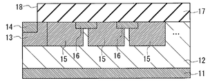
- FIG. 1 is a cross-sectional view showing a configuration of a semiconductor device 1 according to a first embodiment of the present invention.
- the semiconductor device 1 of the present embodiment is a pn diode.
- the semiconductor device 1 includes a silicon carbide (SiC) substrate 11, an SiC epitaxial layer 12, a second conductivity type SiC region 13, an ohmic contact region 14, a junction termination extension (JTE) region 15, a first conductivity type.
- An SiC region 16, a protective film 17, an anode electrode 19 and a cathode electrode 20 are provided.
- the SiC epitaxial layer 12 corresponds to a silicon carbide layer.
- the second conductivity type SiC region 13 corresponds to a second conductivity type region.
- the JTE region 15 corresponds to a junction termination region.
- the first conductivity type SiC region 16 corresponds to the first conductivity type region.
- the SiC substrate 11, the SiC layer that is a semiconductor layer provided on the SiC substrate 11, and the SiC epitaxial layer 12 in this embodiment are collectively referred to as “SiC substrate” or simply “substrate”.
- the substrate is plate-shaped and includes each region formed in SiC epitaxial layer 12, that is, second conductivity type SiC region 13, ohmic contact region 14, JTE region 15, and first conductivity type SiC region 16. .
- outer peripheral edge of the substrate (hereinafter sometimes referred to as “outermost edge”) and the vicinity thereof are shown, and the illustration of the inner part is omitted.
- the right side toward the paper surface corresponds to the outer peripheral end side of the substrate
- the left side toward the paper surface corresponds to the inner side of the outer peripheral edge of the substrate.
- the outer peripheral edge of the substrate corresponds to “the outer peripheral edge of the SiC substrate 11”
- “inner side than the outer peripheral edge of the substrate” corresponds to “inner side of the outer peripheral edge of the SiC substrate 11”.
- the SiC epitaxial layer 12 is provided on the surface of one side in the thickness direction of the SiC substrate 11.
- SiC substrate 11 and SiC epitaxial layer 12 have the first conductivity type.
- the JTE region 15 is formed in the vicinity of the surface on one side in the thickness direction of the SiC epitaxial layer 12.
- the “surface vicinity portion” includes the surface and a portion in the vicinity thereof.
- the semiconductor device 1 includes a plurality of JTE regions 15. Although three JTE regions 15 are illustrated in FIG. 1, four or more JTE regions 15 may be provided.
- the plurality of JTE regions 15 are provided side by side in a direction perpendicular to the thickness direction of the SiC substrate 11 (hereinafter sometimes referred to as “lateral direction”) toward the outermost edge of the semiconductor device 1.
- the horizontal direction is the left-right direction toward the page.
- the plurality of JTE regions 15 are provided adjacent to each other in the horizontal direction.
- “provided adjacent” means to be provided in contact with each other without a gap. Therefore, each JTE region 15 is joined to another JTE region 15 adjacent in the lateral direction.
- the second conductivity type SiC region 13 is formed in a region near the surface on one side in the thickness direction of the SiC epitaxial layer 12 in the region inside the substrate in the lateral direction from the JTE region 15.
- the second conductivity type SiC region 13 is provided in contact with the JTE region 15 provided in the innermost side of the substrate in the lateral direction among the plurality of JTE regions 15.
- Second conductivity type SiC region 13 is formed from the surface on one side in the thickness direction of SiC epitaxial layer 12 to the center in the thickness direction.
- Second conductivity type SiC region 13 has the second conductivity type.
- the ohmic contact region 14 is formed apart from the JTE region 15 in a part of the surface vicinity of one side in the thickness direction of the second conductivity type SiC region 13.
- the ohmic contact region 14 is formed shallower than the second conductivity type SiC region 13.
- the ohmic contact region 14 is formed from the surface on one side in the thickness direction of the second conductivity type SiC region 13 to a depth of about 2/5 (2/5) the depth of the second conductivity type SiC region 13.
- the ohmic contact region 14 has the second conductivity type.
- the impurity concentration of the ohmic contact region 14 is higher than the impurity concentration of the second conductivity type SiC region 13.
- the JTE region (hereinafter sometimes referred to as “internal side JTE region”) 15 provided on the innermost side of the substrate in the lateral direction is adjacent to the second conductivity type SiC region 13 in the lateral direction. Is provided. Specifically, the inner side JTE region 15 is provided adjacent to the second conductivity type SiC region 13 and surrounding the second conductivity type SiC region 13 when viewed from one side in the thickness direction of the substrate. . The other JTE region 15 is provided adjacent to the inner side JTE region 15 and surrounding the inner side JTE region 15 when viewed from one side in the thickness direction of the base.
- the SiC substrate 11 has a rectangular planar shape when viewed from one side in the thickness direction.
- the second conductivity type SiC region 13 is formed along the outer peripheral edge of the SiC substrate 11 so that the planar shape viewed from one side in the thickness direction is an annular shape, specifically a substantially rectangular annular shape.
- Each JTE region 15 is formed along the second conductivity type SiC region 13 so that the planar shape viewed from one side in the thickness direction is an annular shape, specifically, an approximately rectangular annular shape.
- Each JTE region 15 has the second conductivity type.
- the impurity concentration of each JTE region 15 is lower than the impurity concentration of second conductivity type SiC region 13.
- the impurity concentration of each JTE region 15 is stepwise as it goes from the second conductivity type SiC region 13 to the SiC epitaxial layer 12 in the lateral direction, in other words, from the inner side to the outermost edge side in the lateral direction. Has a decreasing concentration distribution.
- the impurity concentration of each JTE region 15 may have a uniform concentration distribution over the entire lateral direction.
- the plurality of JTE regions 15 are arranged side by side from the inner side to the outermost edge side in the descending order of the surface density of the second conductivity type impurities (hereinafter sometimes referred to as “second conductivity type impurities”).
- the plurality of JTE regions 15 are arranged such that the surface density of the second conductivity type impurities decreases from the inner side to the outermost edge side of the substrate.
- the areal density is equal to the integral of the volume impurity density over the thickness of the impurity region.
- the surface density is equal to the product of the volume impurity concentration and the thickness of the impurity region.
- the first conductivity type SiC region 16 is provided in a portion near the surface on one side in the thickness direction of the JTE region 15 where the JTE regions 15 are joined to each other (hereinafter sometimes referred to as “joint portion”). .
- the first conductivity type SiC region 16 is provided across two JTE regions 15 adjacent in the lateral direction.
- the first conductivity type SiC region 16 is provided at each junction of the plurality of JTE regions 15. That is, the semiconductor device 1 includes a plurality of first conductivity type SiC regions 16.
- the plurality of first conductivity type SiC regions 16 are provided side by side at predetermined intervals in the lateral direction.
- Each first conductivity type SiC region 16 is formed shallower than the JTE region 15.
- each first conductivity type SiC region 16 is formed from the surface on one side in the thickness direction of JTE region 15 to a depth of about one third (1/3) of the thickness of JTE region 15.
- Each first conductivity type SiC region 16 has a first conductivity type.
- the protective film 17 is provided on the surface of one side in the thickness direction of the SiC epitaxial layer 12.
- the protective film 17 has an opening 18 at a position corresponding to the region where the ohmic contact region 14 is formed.
- the opening 18 is formed with an opening that opens to one side in the thickness direction of the substrate.
- the ohmic contact region 14 is exposed to one side in the thickness direction through the opening formed in the opening 18.
- the anode electrode 19 is provided in the opening of the opening 18 of the protective film 17.
- the anode electrode 19 is provided in contact with the ohmic contact region 14.
- the anode electrode 19 is electrically connected to the second conductivity type SiC region 13 through the ohmic contact region 14.
- the cathode electrode 20 is provided on the surface of the SiC substrate 11 on the other side in the thickness direction. As shown in FIG. 1, the cathode electrode 20 is provided to face the anode electrode 19.
- the first conductivity type is n-type
- the second conductivity type is p-type. Therefore, SiC substrate 11, SiC epitaxial layer 12 and first conductivity type SiC region 16 have n-type conductivity, and second conductivity type SiC region 13, ohmic contact region 14 and JTE region 15 have p-type conductivity. Have sex.
- the first conductivity type SiC region 16 exists in the vicinity of the surface on one side in the thickness direction among the joint portions of the JTE regions 15 and the second conductivity type SiC.
- Region 13 exists from the surface on one side in the thickness direction of SiC epitaxial layer 12 to a position deeper than first conductivity type SiC region 16.
- the high breakdown voltage semiconductor device 1 that can obtain a stable breakdown voltage can be realized.
- each element is set to the following values assuming that a semiconductor device with a withstand voltage of 3300 V, specifically, a pn diode is manufactured.
- the impurity concentration of SiC epitaxial layer 12 is 3 ⁇ 10 15 / cm 3, and the dimension in the thickness direction (hereinafter referred to as “thickness”) is 30 ⁇ m. Further, the impurity concentration of the second conductivity type SiC region 13 is set to 3 ⁇ 10 18 / cm 3 , and the thickness, that is, the depth from one surface in the thickness direction of the SiC epitaxial layer 12 is set to 0.8 ⁇ m or less. Further, three JTE regions 15 are formed as JTE regions, and the injection surface densities toward the outermost edge are 1.2 ⁇ 10 13 / cm 2 , 7.8 ⁇ 10 12 / cm 2 , and 3.9 ⁇ 10, respectively. 12 / cm 2 .
- “Implanted surface density” is the surface density of impurities during ion implantation.
- the thickness of each JTE region 15, that is, the depth from the surface on one side in the thickness direction of SiC epitaxial layer 12 is set to 0.8 ⁇ m or less.
- the JTE region 15 is formed with an implantation profile in which the impurity concentration is constant over the depth direction of the JTE region 15.
- the second type of JTE structure has an implantation profile in which the impurity concentration in the vicinity of the surface on one side in the thickness direction of the JTE region 15 is lower than the implantation peak that is the peak of the impurity concentration at the time of ion implantation. Is formed. That is, in the second type of JTE structure, the concentration of the second conductivity type impurity in each JTE region 15 has a maximum value on the other side in the thickness direction than the surface on one side in the thickness direction of each JTE region 15. In the second type of JTE structure, a first conductivity type SiC region 16 is formed in the vicinity of the surface of the junction between the JTE regions 15. That is, the second type of JTE structure is the JTE structure in the semiconductor device 1 of the present embodiment.
- the impurity concentration of the first conductivity type SiC region 16 in the second type JTE structure is 1 ⁇ 10 17 / cm 3 , and the thickness, that is, the depth from the surface on one side in the thickness direction of the SiC epitaxial layer 12 is 0.1 ⁇ m.
- the second type of JTE structure may be referred to as “this JTE structure A”, and the first type of JTE structure may be referred to as “comparative JTE structure B”.
- these may be collectively referred to as “JTE structures A and B”.
- the surface on one side in the thickness direction of SiC epitaxial layer 12 may be referred to as “substrate surface S0”. It is assumed that a relatively high reverse voltage of 3300 V is applied to the pn diode that is the semiconductor device 1 in which these two types of JTE structures A and B are formed.
- FIG. 2 is a graph showing the relationship between the electric field intensity reaching the substrate surface S0 and the distance from the second conductivity type SiC region 13 in two types of JTE structures.
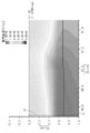
- 3 and 4 are diagrams showing simulation results of the electric field distribution.
- FIG. 3 is a diagram showing a simulation result of the comparative JTE structure B
- FIG. 4 is a diagram showing a simulation result of the present JTE structure A.
- the horizontal axis indicates the distance from the second conductivity type SiC region 13
- the vertical axis indicates the electric field strength.
- the horizontal axis indicates the distance X [ ⁇ m] from the second conductivity type SiC region 13
- the vertical axis indicates the distance Y [ ⁇ m] from the substrate surface S0.
- the direction of the horizontal axis in FIGS. 2 to 4 corresponds to the horizontal direction of the substrate, that is, the left-right direction toward the paper surface of FIG.
- FIG. 2 shows the electric field reaching the substrate surface S0 as a function of the distance from the second conductivity type SiC region 13 for the two types of JTE structures A and B.
- 3 and 4 show the electric field distribution at the junction between the JTE regions 15 having the highest electric field in the two types of JTE structures A and B.
- the JTE region 15 is formed with an implantation profile such that the impurity concentration on the surface side on the one side in the thickness direction of the JTE region 15 is smaller than the implantation peak.
- the peak value of the electric field intensity reaching the substrate surface S0 at the junction between the JTE regions 15 is 0.96 MV / cm. I found out. From the above results, it can be seen that the following effects can be obtained.
- the JTE region 15 is formed with an implantation profile such that the impurity concentration on the surface side on one side in the thickness direction of the JTE region 15 is smaller than the implantation peak, and the junction portion between the JTE regions 15 is formed.
- region 16 is formed in the surface vicinity part of the thickness direction one side among these.
- the back side of the substrate specifically, a region of the JTE region 15 having a relatively high impurity concentration inside the surface on one side in the thickness direction.
- the electric field is concentrated only (hereinafter sometimes referred to as “high impurity region”).
- the first conductivity type SiC region 16 serves as an electric field shield, and the peak value of the electric field intensity reaching the substrate surface S0 can be reduced. Therefore, creeping discharge outside the substrate is suppressed, so that a reduction in breakdown voltage of the semiconductor device can be prevented, and a high breakdown voltage semiconductor device 1 that can obtain a stable breakdown voltage can be realized.
- the concentration of the second conductivity type impurity on the surface on one side in the thickness direction of each JTE region 15 is preferably 1/10 (1/10) or less of the maximum value in the thickness direction.
- concentration of the second conductivity type impurity on the surface on one side in the thickness direction of each JTE region 15 is reduced.
- the peak value of the electric field intensity reaching the substrate surface can be further reduced as compared with a case where the value is larger than one-tenth of the maximum value in the thickness direction.
- creeping discharge outside the substrate can be further suppressed, so that a reduction in breakdown voltage of the semiconductor device 1 can be prevented more reliably. Therefore, it is possible to realize a high breakdown voltage semiconductor device that can obtain a more stable breakdown voltage.
- the comparative JTE structure B is a structure in which the JTE region 15 is formed with an implantation profile in which the impurity concentration is constant over the depth direction of the JTE region 15.
- the JTE region 15 is formed with an implantation profile such that the impurity concentration in the vicinity of the surface on one side in the thickness direction of the JTE region 15 is lower than the implantation peak that is the peak of the impurity concentration during ion implantation.
- the first conductivity type SiC region 16 is formed in the vicinity of the surface of the joint between the JTE regions 15.
- the inventor of the present application further examined by simulation.
- the impurity concentration of the first conductivity type SiC region 16 formed in the vicinity of the surface of the junction between the JTE regions 15 is intentionally made higher than the impurity concentration of the SiC epitaxial layer 12 that is the drift layer, It has been found that the peak value of the electric field intensity reaching the substrate surface can be drastically reduced.
- each element is set to the following values assuming that a semiconductor device with a withstand voltage of 3300 V, specifically, a pn diode is manufactured.
- the n-type impurity which is the first conductivity type impurity is nitrogen (N).
- the p-type impurity which is the second conductivity type impurity is aluminum (Al).
- the impurity concentration of SiC epitaxial layer 12 is 3 ⁇ 10 15 / cm 3 and the thickness is 30 ⁇ m.
- the impurity concentration of the second conductivity type SiC region 13 is set to 3 ⁇ 10 18 / cm 3 , and the thickness, that is, the depth from the surface on one side in the thickness direction of the SiC epitaxial layer 12 is set to about 1.5 ⁇ m.
- the JTE region 15 three JTE regions 15 are formed side by side in the lateral direction of the base.
- the three JTE regions 15 are formed as a first JTE region 15, a second JTE region 15, and a third JTE region 15 in order from the inner side of the base toward the outermost edge, and the formation conditions of each JTE region 15 are as follows.
- the first JTE region 15 has an implantation energy of 500 keV and an implantation dose of 1.5 ⁇ 10 13 / cm 2 .
- the second JTE region 15 has an implantation energy of 500 keV and an implantation dose of 1.0 ⁇ 10 13 / cm 2 .
- the third JTE region 15 has an implantation energy of 500 keV and an implantation dose of 5.0 ⁇ 10 12 / cm 2 .
- the first type of JTE structure is a structure in which the first conductivity type SiC region 16 is formed in the vicinity of the surface of the joint between the JTE regions 15 (hereinafter sometimes referred to as “the present JTE structure C”).
- the second type of JTE structure is a structure in which the first conductivity type SiC region 16 is not formed in the vicinity of the surface of the junction between the JTE regions 15 (hereinafter sometimes referred to as “comparative JTE structure D”).
- the formation energy of the first conductivity type SiC region 16 is set such that the implantation energy is 75 keV and the implantation dose is 1.0 ⁇ 10 12 / cm 2 .
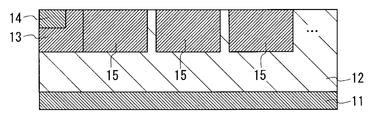
- the first conductivity type SiC region 16 extends over the entire surface vicinity on one side in the thickness direction of the termination region composed of a plurality of JTE regions 15 as shown in FIG. It shall be formed.
- Such a first conductivity type SiC region is indicated by reference numeral “31” in FIG.
- JTE structures C and D may be collectively referred to as “JTE structures C and D”.
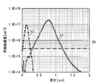
- 5 and 6 are diagrams showing impurity profiles in the thickness direction of the substrate in JTE structures C and D.
- FIG. FIG. 5 is a diagram showing an impurity profile of the comparative JTE structure D
- FIG. 6 is a diagram showing an impurity profile of the present JTE structure C.
- the horizontal axis represents the depth from the substrate surface S0 (hereinafter sometimes simply referred to as “depth”) [ ⁇ m]
- the vertical axis represents the impurity concentration [cm ⁇ 3 ]. .
- the concentration of the first conductivity type impurity in the SiC epitaxial layer 12 is indicated by reference numeral “50”, and among the three JTE regions 15, the first JTE region 15 formed on the innermost side of the base body.
- the concentration of the second conductivity type impurity is indicated by reference numeral “51”.
- the concentration of the first conductivity type impurity in the first conductivity type region 16 is indicated by reference numeral “52”.
- the JTE regions 15 of the JTE structures C and D are formed by performing ion implantation with a single implantation energy as described above. Therefore, the impurity concentration peak of the first JTE region 15 is formed at a position deeper than the substrate surface S0 as shown in FIGS. Specifically, the peak of the impurity concentration of the first JTE region 15 is at a position where the depth from the substrate surface S0 is about 0.8 ⁇ m.
- the concentration is higher than the concentration of aluminum (Al) which is a p-type impurity. Therefore, the first conductivity type SiC region having an impurity concentration equal to or lower than the impurity concentration of SiC epitaxial layer 12 that is the drift layer is deeper on the substrate surface S0 side than JTE region 15. It is formed over about 0.3 ⁇ m.
- the first conductivity type SiC region 16 clearly having an impurity concentration higher than that of the SiC epitaxial layer 12 as the drift layer is higher than the JTE region 15 on the substrate surface S0. On the side, a depth of about 0.3 ⁇ m is formed.
- FIG. 7 is a graph showing the relationship between the electric field intensity reaching the substrate surface S0 and the lateral position of the substrate in the two types of JTE structures C and D.
- the horizontal axis indicates the horizontal position [ ⁇ m] of the substrate
- the vertical axis indicates the electric field strength [MV / cm].
- the lateral position of the substrate is a position in the lateral direction of the substrate.
- the direction of the horizontal axis in FIG. 7 corresponds to the left-right direction toward the plane of FIG.
- the result of the comparative JTE structure D is indicated by the reference sign “60”
- the result of the JTE structure C is indicated by the reference sign “61”.
- the end portion of the second conductivity type SiC region 13, that is, the portion in contact with the JTE region 15 is indicated by an arrow “62”.
- the maximum value of the electric field intensity reaching the substrate surface S0 is 1.44 MV / cm in the comparative JTE structure D, whereas it is 1.02 MV / cm in the present JTE structure C, which is about 30 % Was found to be reduced. That is, the reduction amount ⁇ E of the maximum value of the electric field intensity reaching the substrate surface S0 obtained by changing the comparative JTE structure D to the present JTE structure C was about 30%. From the above results, it can be seen that the following effects can be obtained.
- the impurity concentration higher than that of the SiC epitaxial layer 12 serving as the drift layer is present on the substrate surface S0 side of the JTE region 15 and at least in the vicinity of the surface of the junction portion between the JTE regions 15.
- a one conductivity type SiC region 16 is formed.
- the portion where the electric field strength is highest in the JTE region 15 is the rear side of the JTE region 15, Specifically, it can be positioned on the other side in the thickness direction than the surface on the one side in the thickness direction of the JTE region 15. As a result, the peak value of the electric field intensity reaching the substrate surface S0 can be reduced, so that creeping discharge outside the substrate can be suppressed. Therefore, since a decrease in the breakdown voltage of the semiconductor device 1 can be prevented, a high breakdown voltage semiconductor device 1 that can obtain a stable breakdown voltage can be realized.
- the effect of the first conductivity type SiC region 16 can be obtained in the same manner even when the first conductivity type SiC region 16 is located only in the vicinity of the surface of the joint portion between the JTE regions 15 as shown in FIG. . Further, as shown in FIG. 17 to be described later, the first conductivity type SiC region 16 can be obtained in the same manner even if the structure is located only in the vicinity of the surface of the junction portion between the JTE region 15 and the SiC epitaxial layer 12.
- the effect of the first conductivity type SiC region 16 is that the first conductivity type is present on the substrate surface S0 side relative to the JTE region 15, at least in the vicinity of the surface of the JTE region 15 or between the JTE region 15 and the SiC epitaxial layer 12. If type SiC region 16 is formed, it can be obtained.
- 8 to 13 are views for explaining a method of manufacturing the semiconductor device 1 according to the first embodiment of the present invention.
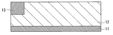
- FIG. 8 is a cross-sectional view showing a state where the formation of the second conductivity type SiC region 13 is completed.
- an epitaxial growth process using a predetermined dopant is performed on the surface of one side in the thickness direction of the SiC substrate 11 having the first conductivity type.
- SiC epitaxial layer 12 having the first conductivity type is formed on the surface on one side in the thickness direction of SiC substrate 11.
- the step of forming SiC epitaxial layer 12 corresponds to a silicon carbide layer forming step.
- an n-type SiC substrate 11 is used as the SiC substrate 11, and a first conductivity type impurity, specifically, an n-type impurity is used as a predetermined dopant.
- nitrogen (N), phosphorus (P), or the like is used as the n-type impurity.
- a process of implanting ions of a predetermined dopant into a region predetermined as a region for forming the second conductivity type SiC region 13 in the vicinity of the surface on one side in the thickness direction of the SiC epitaxial layer 12 (hereinafter referred to as “ion”). In some cases, it is called “injection process”
- an ion implantation process is performed so that ions are implanted from the surface on one side in the thickness direction of SiC epitaxial layer 12 over the central portion in the thickness direction.
- the second conductivity type SiC region having the second conductivity type in a part of the surface vicinity portion on one side in the thickness direction of the SiC epitaxial layer 12, specifically, the predetermined region. 13 is formed.
- the step of forming the second conductivity type SiC region 13 corresponds to a second conductivity type region formation step.
- the ion implantation process in this step for forming the second conductivity type SiC region 13 may be performed with a single implantation energy, or while stepping the implantation energy, for example, stepping from high energy to low energy. You may go while changing.
- a second conductivity type impurity specifically, a p-type impurity is used in this embodiment.
- aluminum (Al) or boron (B) is used as the p-type impurity.
- FIG. 9 is a cross-sectional view showing a state where the formation of the ohmic contact region 14 is completed.
- an ion implantation process is performed on a region that is predetermined as a region for forming the ohmic contact region 14 among the regions where the second conductivity type SiC region 13 is formed.
- an ohmic contact region 14 having an impurity concentration higher than that of the second conductivity type SiC region 13 and having the second conductivity type is formed in the second conductivity type SiC region 13.
- the ion implantation process in this step for forming the ohmic contact region 14 may be performed with a single implantation energy, or while stepping the implantation energy, for example, stepping from high energy to low energy. You may go.
- a p-type impurity is used as the predetermined dopant used in the ion implantation process in this step.
- aluminum (Al) or boron (B) is used as the p-type impurity.
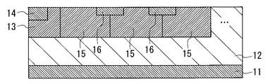
- FIG. 10 is a cross-sectional view showing a state in which the formation of the JTE region 15 has been completed.
- the implantation mask is changed to a region adjacent to the second conductivity type SiC region 13 in the lateral direction of the substrate in the vicinity of the surface on one side in the thickness direction of the SiC epitaxial layer 12.
- a plurality of ion implantation processes are performed.
- a plurality of JTE regions 15 adjacent to the second conductivity type SiC region 13 are formed.
- the plurality of JTE regions 15 are formed side by side in the horizontal direction.
- the step of forming this JTE region 15 corresponds to a termination region forming step. Further, the region adjacent to the second conductivity type SiC region 13 in the lateral direction of the base is the portion on the outer peripheral end side of the SiC substrate 11 relative to the second conductivity type SiC region 13, and the second conductivity type SiC region 13. This corresponds to the area adjacent to.
- Each JTE region 15 is formed to have the second conductivity type.
- Each JTE region 15 is formed so that its impurity concentration is lower than that of second conductivity type SiC region 13. Further, each JTE region 15 has its impurity concentration as it goes from the second conductivity type SiC region 13 to the SiC epitaxial layer 12 in the lateral direction, in other words, from the inner side to the outermost edge side in the lateral direction. It is formed so as to have a concentration distribution that decreases stepwise.
- each JTE region 15 may be formed so that its impurity concentration has a uniform concentration distribution over the entire lateral direction.
- the plurality of JTE regions 15 are formed so that the surface density of the second conductivity type impurities decreases toward the outer peripheral end side of the SiC substrate 11 by adjusting the ion implantation amount in the ion implantation process.
- the ion implantation process in this step for forming the JTE region 15 may be performed with a single implantation energy, or while changing the implantation energy stepwise, for example, while steppingly changing from high energy to low energy. May be.
- ions are implanted deeper as the implantation energy increases. Therefore, when ion implantation is performed with a single implantation energy, an impurity concentration distribution having an impurity concentration peak at a deeper position from the surface on one side in the thickness direction of SiC epitaxial layer 12 is realized as the implantation energy increases. .
- the concentration of the second conductivity type impurity in each JTE region 15 is changed to the one side in the thickness direction of each JTE region 15.
- Each JTE region 15 is formed to have a maximum value on the other side in the thickness direction from the surface.
- an impurity of the second conductivity type specifically, a p-type impurity is used in this embodiment.
- a p-type impurity is used as the predetermined dopant used in the ion implantation process in this step.
- aluminum (Al) or boron (B) is used as the p-type impurity.
- FIG. 11 is a cross-sectional view showing a state where the formation of the first conductivity type SiC region 16 has been completed.
- the JTE region 15 is formed, at least a portion near the surface on one side in the thickness direction of the portion where the JTE regions 15 are joined is subjected to an ion implantation process.
- Ion implantation treatment is performed in the vicinity of the surface on one side in the thickness direction of the part where the JTE regions 15 are joined.
- the first conductivity type SiC region 16 is formed at the joint portion of the JTE region 15 in the vicinity of the surface on one side in the thickness direction of the JTE region 15.
- the first conductivity type SiC region 16 is formed, for example, from the surface on one side in the thickness direction of the JTE region 15 to a depth of one third (1/3) of the thickness of the JTE region 15.
- the step of forming the first conductivity type SiC region 16 corresponds to the first conductivity type region formation step.
- the surface of one side in the thickness direction of the SiC epitaxial layer 12, specifically, one side in the thickness direction of the JTE region 15 is adjusted by adjusting the implantation energy in the ion implantation process.
- the first conductivity type SiC region 16 can be formed from the surface to a depth not reaching the bottom of the JTE region 15. Accordingly, as shown in FIG. 11, the first conductivity type SiC region 16 exists in the vicinity of the surface on one side in the thickness direction among the joint portions of the JTE regions 15, and the second conductivity type SiC region 13 is
- the SiC epitaxial layer 12 may be formed from the surface on one side in the thickness direction to a position deeper than the first conductivity type SiC region 16.
- each impurity ion-implanted in each process described above can be electrically activated. Further, the crystallinity of the ion implantation region can be recovered together by the activation annealing treatment.
- FIG. 12 is a cross-sectional view showing a state in which the formation of the protective film 17 has been completed.
- a protective film 17 is formed on the surface of one side in the thickness direction of the SiC epitaxial layer 12 as shown in FIG.
- the protective film 7 is realized by an insulating film made of an insulating material such as SiO 2 or polyimide.
- FIG. 13 is a cross-sectional view showing a state in which the formation of the opening 18 has been completed. After the protective film 17 is formed, an opening 18 is formed in the protective film 17 as shown in FIG. As shown in FIG. 13, the opening 18 is formed so that the ohmic contact region 14 is exposed from the bottom of the opening 18.
- the anode electrode 19 shown in FIG. 1 is formed so as to be electrically connected to the ohmic contact region 14 exposed from the bottom of the opening 18. Further, the cathode electrode 20 shown in FIG. 1 is formed on the surface on the other side in the thickness direction of the SiC substrate 11.
- the semiconductor device 1 according to the first embodiment of the present invention shown in FIG. 1 is obtained.
- the first conductivity type SiC region 16 is present in the vicinity of the surface on one side in the thickness direction
- the second conductivity type SiC region 13 is the SiC epitaxial layer.
- Semiconductor device 1 existing from the surface on one side in the thickness direction of 12 to a position deeper than first conductivity type SiC region 16 can be obtained.
- the semiconductor device 1 having such a configuration when a relatively high reverse voltage is applied to the pn junction as described above, the electric field is concentrated on the junction portion of the adjacent JTE region 15 and the peak of the electric field strength is generated. Even in this case, the peak value of the electric field strength reaching the surface on one side in the thickness direction of SiC epitaxial layer 12 can be reduced. Therefore, according to the manufacturing method of the semiconductor device of the present embodiment, it is possible to provide the high breakdown voltage semiconductor device 1 that can obtain a stable breakdown voltage.
- the impurity concentration distribution in the JTE region 15 is adjusted by adjusting the implantation energy in the ion implantation process. Therefore, by using, for example, one type of ion implantation energy, the high breakdown voltage semiconductor device 1 that can obtain a stable breakdown voltage as described above can be easily manufactured.
- the first conductivity type SiC region 16 is formed by forming the JTE region 15 by ion implantation and then performing ion implantation.
- the first conductivity type SiC region may be formed by other formation methods.
- FIG. 14 is a cross-sectional view showing another example of the first conductivity type SiC region.
- FIG. 14 shows a state in which the formation of the first conductivity type SiC region 26 which is another example of the first conductivity type SiC region is completed.
- the first conductivity type SiC region 26 may be formed by using a lateral spreading effect at the time of ion implantation for forming the JTE region 25.
- the adjacent JTE region 25 is formed on the SiC epitaxial layer 12 by adjusting the position where ions are implanted, using the lateral spreading effect at the time of ion implantation.
- the connection is made at a position deeper than the surface on one side in the thickness direction.
- a portion where the JTE regions 25 are not connected to each other is formed in the vicinity of the surface on one side in the thickness direction of the SiC epitaxial layer 12.
- the JTE region 25 corresponds to a junction termination region.
- the first conductivity type SiC region 26 corresponds to the first conductivity type region. Even with the structure as shown in FIG. 14, the same effect as the present embodiment can be obtained.
- the first conductivity type SiC region 26 is indicated by hatching different from that of the SiC epitaxial layer 12, but is actually the same. As described above, the SiC epitaxial layer 12 remaining between the JTE regions 25 after the ion implantation process for forming the JTE regions 25 becomes the first conductivity type SiC region 26.
- the first conductivity type SiC region 26 is formed by using the lateral spreading effect at the time of ion implantation for forming the JTE region 25, thereby performing the ion implantation process for forming the first conductivity type SiC region 26. This process can be omitted. Therefore, as described above, a high breakdown voltage semiconductor device capable of obtaining a stable breakdown voltage can be manufactured more easily and inexpensively as compared with the present embodiment.
- the first conductivity type SiC region 26 may be formed by connecting adjacent JTE regions 25 at a position deeper than the surface on one side in the thickness direction of the SiC epitaxial layer 12 by another method.
- another method for example, a method of tapering a resist serving as an implantation mask or a method of performing ion implantation processing on the SiC substrate 11 from an oblique direction can be used. Even when the first conductivity type SiC region 26 is formed in this manner, the same effects as in the present embodiment can be obtained.
- the SiC epitaxial layer 12 is subjected to ion implantation processing in order to form the JTE region 15.
- the average value of the implantation surface density over the entire terminal implantation region constituted by the plurality of JTE regions 15 adjacent to the second conductivity type SiC region 13 is 0.5. as a ⁇ 10 13 / cm 2 ⁇ 3 ⁇ 10 13 / cm 2, it is desirable to perform an ion implantation process.
- the implantation surface density is equal to the integral of the volume impurity density over the thickness of the impurity region. When the volume impurity concentration is constant over the thickness of the impurity region, the implantation surface density is equal to the product of the volume impurity concentration and the thickness of the impurity region.
- the thickness of each JTE region 15, that is, the depth from the surface on one side in the thickness direction of SiC epitaxial layer 12 is about 0.6 ⁇ m to 1.0 ⁇ m.
- the injection width of each JTE region 15 is about 30 ⁇ m to 300 ⁇ m.
- the impurity concentration of the first conductivity type SiC region 16 is about 10 16 / cm 3 to 10 17 / cm 3 , and its thickness, that is, the depth from the surface on one side in the thickness direction of the SiC epitaxial layer 12 is 0 It is about 1 ⁇ m to 0.3 ⁇ m.
- the semiconductor device 1 is a pn diode
- the semiconductor device 1 is not limited to the pn diode, and any semiconductor device 1 having the JTE region 15 as a termination structure may be used.
- Configuration can be applied.
- the configuration of the semiconductor device 1 of the present embodiment is also applied to a Schottky diode using SiC, a MOSFET using SiC, an insulated gate bipolar transistor (Insulated Gate Bipolar Transistor) using SiC, and the like. can do.
- the implantation profile for forming the JTE region 15 is such that the impurity concentration in the vicinity of the surface on one side in the thickness direction of the JTE region 15 is smaller than the implantation peak.
- a first conductivity type SiC region 16 exists in the vicinity of the surface on one side in the thickness direction of the joint portion between the JTE regions 15.
- second conductivity type SiC region 13 exists from the surface on one side in the thickness direction of SiC epitaxial layer 12 to a position deeper than first conductivity type SiC region 16.
- Such a configuration can also be applied to a semiconductor device using SiC having the JTE region 15, such as a Schottky diode, a MOSFET, or an IGBT.
- the structure in which the first conductivity type SiC region 16 is located only in the vicinity of the surface of the joint portion of the adjacent JTE region 15 has been described.
- the first conductivity type SiC region has another structure. It may be.
- 15 and 16 are cross-sectional views showing other examples of the first conductivity type SiC region.
- 15 and 16 show a state where the formation of the first conductivity type SiC regions 31 and 32, which are other examples of the first conductivity type SiC region, is completed.
- the first conductivity type SiC regions 31 and 32 correspond to the first conductivity type region.
- the first conductivity type SiC region is formed over the entire surface vicinity on one side in the thickness direction of the termination region composed of a plurality of JTE regions 15, as in the first conductivity type SiC region 31 shown in FIG. 15. Also good. Further, the first conductivity type SiC region is one side in the thickness direction of the device including the second conductivity type SiC region 13 and the ohmic contact region 14 in addition to the termination region, like the first conductivity type SiC region 32 shown in FIG. It may be formed over the entire surface vicinity. Even with the structure as shown in FIG. 15 and FIG. 16, the same effect as in the present embodiment can be obtained.
- FIG. 17 is a cross-sectional view showing the configuration of the semiconductor device 2 according to the second embodiment of the present invention.
- the semiconductor device 2 of the present embodiment is similar in configuration to the semiconductor device 1 of the first embodiment described above. Therefore, in the present embodiment, portions different from the semiconductor device 1 of the first embodiment will be described, and portions corresponding to the semiconductor device 1 will be denoted by the same reference numerals and common description will be omitted. Also in the present embodiment, the first conductivity type is n-type and the second conductivity type is p-type, as in the first embodiment.
- the semiconductor device 2 of the present embodiment is a pn diode, like the semiconductor device 1 of the first embodiment described above. Similar to the semiconductor device 1 of the first embodiment, the semiconductor device 2 of the present embodiment has a silicon carbide (SiC) substrate 11, a SiC epitaxial layer 12, a second conductivity type SiC region 13, an ohmic contact region. 14, a JTE region 15, a first conductivity type SiC region 16, a protective film 17, an anode electrode 19, and a cathode electrode 20.
- SiC silicon carbide
- a plurality of JTE regions 15 are provided adjacent to each other in the lateral direction toward the outermost edge of the semiconductor device 1. ing.
- a plurality of JTE regions 15 are spaced apart from each other in the horizontal direction toward the outermost edge of the semiconductor device 2. Is provided. That is, the plurality of JTE regions 15 are provided apart from each other and are not in contact with each other.
- An SiC epitaxial layer 12 is interposed between adjacent JTE regions 15.
- the first conductivity type SiC region 16 is formed in the vicinity of the surface on one side in the thickness direction of the JTE region 15 and the SiC epitaxial layer 12 in the joint portion between the JTE region 15 and the SiC epitaxial layer 12.
- 18 to 21 are views for explaining a method of manufacturing the semiconductor device 2 according to the second embodiment of the present invention.
- the first conductivity type is formed on the surface of one side in the thickness direction of the SiC substrate 11 having the first conductivity type in the same manner as in the first embodiment.
- a SiC epitaxial layer 12 is formed.
- the second conductivity type SiC region 13 having the second conductivity type is preliminarily defined as a region for forming second conductivity type SiC region 13.
- a region predetermined as a region where the ohmic contact region 14 is formed is transferred from the second conductivity type SiC region 13.
- the ohmic contact region 14 having a high impurity concentration and having the second conductivity type is formed.
- FIG. 18 is a cross-sectional view showing a state where the formation of the JTE region 15 has been completed.
- a plurality of ion implantation processes are performed on the region adjacent to the second conductivity type SiC region 13 in the lateral direction while changing the implantation mask to form a plurality of JTE regions 15.
- a plurality of JTE regions 15 are formed at predetermined intervals toward the outermost edge. That is, the plurality of JTE regions 15 are formed such that the SiC epitaxial layer 12 is interposed between the adjacent JTE regions 15 apart from each other.
- the step of forming the JTE region 15 corresponds to a termination region forming step.
- Each JTE region 15 is formed to have the second conductivity type.
- Each JTE region 15 is formed such that its impurity concentration is lower than the impurity concentration of second conductivity type SiC region 13. Further, each JTE region 15 has a concentration distribution that decreases stepwise as it goes from the second conductivity type SiC region 13 to the SiC epitaxial layer 12, in other words, from the inside of the substrate toward the outermost edge in the lateral direction. Formed. Although different from the present embodiment, it may be formed to have a uniform concentration distribution.
- the ion implantation process in this step for forming the JTE region 15 may be performed with a single implantation energy, for example, with a high energy while changing the implantation energy stepwise. It may be performed while gradually changing from low energy to low energy.
- ions are implanted deeper as the implantation energy increases. Therefore, when ion implantation is performed with a single implantation energy, an impurity concentration distribution having an impurity concentration peak at a deeper position from the surface on one side in the thickness direction of SiC epitaxial layer 12 is realized as the implantation energy increases. .
- FIG. 19 is a cross-sectional view showing a state where the formation of the first conductivity type SiC region 16 is completed.
- an ion implantation process is performed on a portion where the JTE region 15 and the SiC epitaxial layer 12 are joined at least in the vicinity of the surface on one side in the thickness direction of the JTE region 15 and the SiC epitaxial layer 12. Apply.
- an ion implantation process is performed on a portion where the JTE region 15 and the SiC epitaxial layer 12 are joined in the vicinity of the surface on one side in the thickness direction of the JTE region 15 and the SiC epitaxial layer 12.
- First conductivity type SiC region 16 is formed, for example, from the surface on one side in the thickness direction of JTE region 15 and SiC epitaxial layer 12 to a depth of one third (1/3) of the thickness of JTE region 15. .
- the step of forming the first conductivity type SiC region 16 corresponds to the first conductivity type region formation step.
- the surface of one side in the thickness direction of the SiC epitaxial layer 12, specifically, one side in the thickness direction of the JTE region 15 is adjusted by adjusting the implantation energy of the ion implantation process.
- the first conductivity type SiC region 16 can be formed from the surface to a depth not reaching the bottom of the JTE region 15. As a result, as shown in FIG.
- the first conductivity type SiC region 16 exists in the vicinity of the surface on one side in the thickness direction in the portion where the JTE region 15 and the SiC epitaxial layer 12 are joined, and the first The two-conductivity type SiC region 13 may be formed from the surface on one side in the thickness direction of the SiC epitaxial layer 12 to a position deeper than the first conductivity type SiC region 16.
- an activation annealing process is performed in the same manner as in the first embodiment. Thereby, each impurity ion-implanted in each process described above can be electrically activated. Further, the crystallinity of the ion implantation region can be recovered together by the activation annealing treatment.
- FIG. 20 is a cross-sectional view showing a state in which the formation of the protective film 17 has been completed.
- protective film 17 is formed on the surface of one side in the thickness direction of SiC epitaxial layer 12, as shown in FIG. 20, as in the first embodiment. To do.
- the protective film 17 is realized by an insulating film made of an insulating material such as SiO 2 or polyimide.
- FIG. 21 is a cross-sectional view showing a state where the formation of the opening 18 has been completed. After the protective film 17 is formed, an opening 18 is formed in the protective film 17 as shown in FIG. As shown in FIG. 21, the opening 18 is formed such that the ohmic contact region 14 is exposed from the bottom of the opening 18.
- the anode shown in FIG. 17 is electrically connected to the ohmic contact region 14 exposed from the bottom of the opening 18 in the same manner as in the first embodiment.
- the electrode 19 is formed.
- the cathode electrode 20 shown in FIG. 17 is formed on the surface of the other side in the thickness direction of the SiC substrate 11.
- the semiconductor device 2 according to the second embodiment of the present invention is obtained.
- the first conductivity type SiC region 16 exists in the vicinity of the surface on one side in the thickness direction at the junction portion between the JTE region 15 and the SiC epitaxial layer 12, and the second conductivity type SiC region 13 is made of SiC.
- Semiconductor device 2 existing from the surface on one side in the thickness direction of epitaxial layer 12 to a position deeper than first conductivity type SiC region 16 can be obtained.
- the same effect as that described in the first embodiment can be obtained. That is, even when a relatively high reverse voltage is applied to the pn junction, the electric field concentrates on the portion where the JTE region 15 and the SiC epitaxial layer 12 are joined, and even if the electric field strength peak occurs, the SiC epitaxial layer The peak value of the electric field intensity reaching the surface on one side in the thickness direction can be reduced. Therefore, the high breakdown voltage semiconductor device 2 that can obtain a stable breakdown voltage can be provided.
- the configuration of the semiconductor device 2 according to the present embodiment is not limited to the pn diode as long as it has the JTE region 15 as a termination structure. Can be applied.
- the configuration of the present embodiment can also be applied to a SiC Schottky diode, a SiC MOSFET, a SiC IGBT, and the like.
- the implantation profile for forming the JTE region 15 is such that the impurity concentration in the vicinity of the surface on one side in the thickness direction of the JTE region 15 is smaller than the implantation peak, and the JTE region 15 and the SiC epitaxial layer 12
- the first conductivity type SiC region 16 exists in the vicinity of the surface on the one side in the thickness direction of the junction with the second conductivity type SiC region 13 from the surface on the one side in the thickness direction of the SiC epitaxial layer 12.
- the configuration that exists deeper than the type SiC region 16 can also be applied to a SiC Schottky diode, a SiC MOSFET, a SiC IGBT, or the like having the JTE region 15.
- first conductivity type SiC region 16 is located only in the vicinity of the surface of the junction portion between JTE region 15 and SiC epitaxial layer 12 has been described.
- other structures may be used. .
- 22 and 23 are cross-sectional views showing other examples of the first conductivity type SiC region. 22 and 23 show a state where the formation of the first conductivity type SiC regions 31 and 32, which are the first conductivity type SiC regions, is completed.
- the first conductivity type SiC region is formed over the entire surface vicinity on one side in the thickness direction of the termination region composed of a plurality of JTE regions 15 as in the first conductivity type SiC region 31 shown in FIG. Also good.
- the first conductivity type SiC region may be formed over the entire surface vicinity of the device including the second conductivity type SiC region 13 and the ohmic contact region 14 shown in FIG. Even with the structure as shown in FIGS. 22 and 23, the same effect as in the present embodiment can be obtained.
- each JTE region 15, 25 has a lower concentration of the second conductivity type impurity than that of the second conductivity type SiC region 13.
- the electric field strength in the JTE regions 15 and 25 can be reduced, so that creeping discharge outside the substrate can be more reliably suppressed. Therefore, it is possible to more reliably prevent the breakdown voltage of the semiconductor device from decreasing.
- the plurality of JTE regions 15 and 25 are arranged such that the concentration of the second conductivity type impurity decreases in the lateral direction from the inner side of the substrate toward the outermost edge side. Has been. Thereby, the electric field strength in the JTE regions 15 and 25 can be lowered toward the outermost edge side of the substrate, so that creeping discharge outside the substrate can be further reliably suppressed. Therefore, it is possible to more reliably prevent the breakdown voltage of the semiconductor device from decreasing.
- the JTE regions 15 and 25 may be formed such that the concentration of the second conductivity type impurity is equal to that of the second conductivity type SiC region 13.
- the second conductivity type SiC region 13 and the JTE regions 15 and 25 can be formed in the same process, so that a high breakdown voltage semiconductor device capable of obtaining a stable breakdown voltage as described above can be easily manufactured. can do.
- the inner side JTE regions 15 and 25 formed on the innermost side of the base in the lateral direction are the second conductive regions in the lateral direction. It is formed adjacent to type SiC region 13.
- the inner JTE regions 15 and 25 may be formed separately from the second conductivity type SiC region 13 in the lateral direction. That is, the inner side JTE regions 15 and 25 and the second conductivity type SiC region 13 may be formed apart from each other in the lateral direction. Even when configured in this way, the same effects as those of the first and second embodiments can be obtained.
- the first conductivity type is n-type and the second conductivity type is p-type.
- the first conductivity type is p-type and the second conductivity type is It may be n-type.
- SiC substrate 11, SiC epitaxial layer 12 and first conductivity type SiC region 16 have p-type conductivity
- second conductivity type SiC region 13, ohmic contact region 14 and JTE region 15 have n-type conductivity. It has the conductivity of.
Landscapes
- Electrodes Of Semiconductors (AREA)
- Recrystallisation Techniques (AREA)
Abstract
Description
図1は、本発明の第1の実施の形態である半導体装置1の構成を示す断面図である。本実施の形態の半導体装置1は、pnダイオードである。半導体装置1は、炭化珪素(SiC)基板11、SiCエピタキシャル層12、第2導電型SiC領域13、オーミックコンタクト領域14、接合終端延長(Junction Termination Extension;略称:JTE)領域15、第1導電型SiC領域16、保護膜17、アノード電極19およびカソード電極20を備えて構成される。
図17は、本発明の第2の実施の形態である半導体装置2の構成を示す断面図である。本実施の形態の半導体装置2は、前述の第1の実施の形態の半導体装置1と構成が類似している。したがって本実施の形態では、第1の実施の形態の半導体装置1と異なる部分について説明し、半導体装置1に対応する部分については同一の参照符を付して、共通する説明を省略する。本実施の形態においても、前述の第1の実施の形態と同様に、第1の導電型をn型とし、第2の導電型をp型とする。
Claims (11)
- 第1の導電型を有する炭化珪素基板(11)と、
前記炭化珪素基板(11)の厚み方向一方側の表面上に設けられ、第1の導電型を有する炭化珪素層(12)と、
前記炭化珪素層(12)の厚み方向一方側の表面近傍部の一部分に形成され、第2の導電型を有する第2導電型領域(13)と、
前記炭化珪素層(12)の厚み方向一方側の表面近傍部のうち、前記第2導電型領域(13)よりも前記炭化珪素基板(11)の外周端側の部分に形成され、第2の導電型を有する複数の接合終端領域(15,25)とを備え、
前記複数の接合終端領域(15,25)は、少なくとも前記炭化珪素層(12)の厚み方向一方側の表面で互いに隣接または離間して形成され、
少なくとも、前記接合終端領域(15)同士が接合している部分または離間する前記接合終端領域(15,25)同士の間の部分の厚み方向一方側の表面近傍部には、第1の導電型を有し、前記炭化珪素層(12)よりも第1の導電型の不純物の濃度が高い第1導電型領域(16,26,31,32)が形成されていることを特徴とする半導体装置。 - 前記複数の接合終端領域(25)は、前記炭化珪素層(12)の厚み方向一方側の表面では互いに離間し、前記表面よりも前記炭化珪素層(12)の厚み方向他方側では連結して形成されることを特徴とする請求項1に記載の半導体装置。
- 各前記接合終端領域(15,25)は、第2の導電型の不純物の濃度が、前記第2導電型領域(13)と等しいことを特徴とする請求項1に記載の半導体装置。
- 各前記接合終端領域(15,25)は、前記第2の導電型の不純物の濃度が、前記第2導電型領域(13)よりも低いことを特徴とする請求項1に記載の半導体装置。
- 前記複数の接合終端領域(15,25)は、前記第2の導電型の不純物の濃度が、前記炭化珪素基板(11)の外周端側に向かうにつれて減少するように配置されることを特徴とする請求項1に記載の半導体装置。
- 各前記接合終端領域(15,25)における前記第2の導電型の不純物濃度は、厚み方向一方側の表面よりも厚み方向他方側で最大値となることを特徴とする請求項1に記載の半導体装置。
- 各前記接合終端領域(15,25)は、厚み方向一方側の表面における前記第2の導電型の不純物の濃度が、前記最大値の10分の1以下であることを特徴とする請求項6に記載の半導体装置。
- 第1の導電型を有する炭化珪素基板(11)の厚み方向一方側の表面上に、第1の導電型を有する炭化珪素層(12)を形成する炭化珪素層形成工程と、
前記炭化珪素層(12)の厚み方向一方側の表面近傍部の一部分に、第2の導電型を有する第2導電型領域(13)を形成する第2導電型領域形成工程と、
前記炭化珪素層(12)の厚み方向一方側の表面近傍部のうち、前記第2導電型領域(13)よりも前記炭化珪素基板(11)の外周端側の部分に、イオン注入処理を施すことによって、第2の導電型を有する複数の接合終端領域(15,25)を少なくとも前記炭化珪素層(12)の厚み方向一方側の表面で互いに隣接または離間するように形成する終端領域形成工程と、
少なくとも、前記接合終端領域(15)同士が接合している部分または離間する前記接合終端領域(15,25)同士の間の部分の厚み方向一方側の表面近傍部に、イオン注入処理を施すことによって、第1の導電型を有し、前記炭化珪素層(12)よりも第1の導電型の不純物の濃度が高い第1導電型領域(16,26,31,32)を形成する第1導電型領域形成工程とを備えることを特徴とする半導体装置の製造方法。 - 前記終端領域形成工程では、
前記複数の接合終端領域(25)を、前記炭化珪素層(12)の厚み方向一方側の表面では互いに離間し、前記表面よりも前記炭化珪素層(12)の厚み方向他方側では連結されるように形成することを特徴とする請求項8に記載の半導体装置の製造方法。 - 前記終端領域形成工程では、前記イオン注入処理におけるイオン注入量を調整することによって、前記複数の接合終端領域(15,25)における第2の導電型の不純物の濃度が、前記炭化珪素基板(11)の外周端側に向かうにつれて減少するように、前記複数の接合終端領域(15,25)を形成することを特徴とする請求項8に記載の半導体装置の製造方法。
- 前記終端領域形成工程では、前記イオン注入処理におけるイオン注入量を調整することによって、各前記接合終端領域(15,25)における第2の導電型の不純物の濃度が、前記炭化珪素層(12)の厚み方向一方側の表面よりも前記炭化珪素層(12)の厚み方向他方側で最大値となるように、各前記接合終端領域(15,25)を形成することを特徴とする請求項8に記載の半導体装置の製造方法。
Priority Applications (4)
| Application Number | Priority Date | Filing Date | Title |
|---|---|---|---|
| US14/009,628 US8866158B2 (en) | 2011-04-04 | 2012-03-29 | Semiconductor device and method for manufacturing same |
| JP2013508830A JP5697744B2 (ja) | 2011-04-04 | 2012-03-29 | 半導体装置およびその製造方法 |
| CN201280015311.4A CN103460392B (zh) | 2011-04-04 | 2012-03-29 | 半导体装置及其制造方法 |
| DE112012001565.7T DE112012001565B4 (de) | 2011-04-04 | 2012-03-29 | Halbleitervorrichtungen und Verfahren zur Herstellung derselben |
Applications Claiming Priority (2)
| Application Number | Priority Date | Filing Date | Title |
|---|---|---|---|
| JP2011082386 | 2011-04-04 | ||
| JP2011-082386 | 2011-04-04 |
Publications (1)
| Publication Number | Publication Date |
|---|---|
| WO2012137659A1 true WO2012137659A1 (ja) | 2012-10-11 |
Family
ID=46969060
Family Applications (1)
| Application Number | Title | Priority Date | Filing Date |
|---|---|---|---|
| PCT/JP2012/058375 Ceased WO2012137659A1 (ja) | 2011-04-04 | 2012-03-29 | 半導体装置およびその製造方法 |
Country Status (5)
| Country | Link |
|---|---|
| US (1) | US8866158B2 (ja) |
| JP (1) | JP5697744B2 (ja) |
| CN (1) | CN103460392B (ja) |
| DE (1) | DE112012001565B4 (ja) |
| WO (1) | WO2012137659A1 (ja) |
Cited By (7)
| Publication number | Priority date | Publication date | Assignee | Title |
|---|---|---|---|---|
| JP2014207444A (ja) * | 2013-03-26 | 2014-10-30 | インフィネオン テクノロジーズ アーゲーInfineon Technologies Ag | 炭化珪素装置および炭化珪素装置の形成方法 |
| GB2517285A (en) * | 2013-07-02 | 2015-02-18 | Gen Electric | Semiconductor devices and methods of manufacture |
| WO2015198718A1 (ja) * | 2014-06-23 | 2015-12-30 | 住友電気工業株式会社 | 炭化珪素半導体装置およびその製造方法 |
| JP2016025300A (ja) * | 2014-07-24 | 2016-02-08 | 株式会社日立製作所 | 高耐圧半導体装置 |
| JPWO2017043608A1 (ja) * | 2015-09-09 | 2018-06-28 | 住友電気工業株式会社 | 半導体装置 |
| JP2019096878A (ja) * | 2017-11-24 | 2019-06-20 | インフィネオン テクノロジーズ アーゲーInfineon Technologies Ag | エッジ終端構造を有するシリコンカーバイド半導体部品 |
| JP2024500968A (ja) * | 2020-12-23 | 2024-01-10 | セミコンダクター・コンポーネンツ・インダストリーズ・リミテッド・ライアビリティ・カンパニー | 動的出力容量損失が低減された終端構造 |
Families Citing this family (10)
| Publication number | Priority date | Publication date | Assignee | Title |
|---|---|---|---|---|
| CN105493293B (zh) * | 2013-09-09 | 2018-08-24 | 株式会社日立制作所 | 半导体装置及其制造方法 |
| TWI544622B (zh) * | 2015-06-05 | 2016-08-01 | 國立清華大學 | 半導體結構 |
| JP6873926B2 (ja) | 2015-06-09 | 2021-05-19 | アーベーベー・シュバイツ・アーゲーABB Schweiz AG | 炭化ケイ素パワー半導体デバイスのエッジ終端部を製造する方法 |
| US10141851B2 (en) * | 2016-03-25 | 2018-11-27 | General Electric Company | Resonant DC to DC power converter |
| WO2018074228A1 (ja) * | 2016-10-18 | 2018-04-26 | 株式会社デンソー | 半導体装置およびその製造方法 |
| EP3975266A1 (en) * | 2020-09-28 | 2022-03-30 | Nexperia B.V. | Semiconductor device with improved junction termination extension region |
| CN115911097A (zh) * | 2022-12-31 | 2023-04-04 | 厦门大学 | 一种用于SiC功率器件的复合终端结构及其制造方法 |
| EP4404268A1 (en) * | 2023-01-20 | 2024-07-24 | Nexperia B.V. | Semiconductor device with improved control of surface charges in termination |
| EP4531107A1 (en) * | 2023-09-27 | 2025-04-02 | Nexperia B.V. | Improved top surface of a junction termination extension for semiconductor devices |
| EP4531108A1 (en) * | 2023-09-27 | 2025-04-02 | Nexperia B.V. | Improved recessed regions of a junction termination extension for semiconductor devices |
Citations (2)
| Publication number | Priority date | Publication date | Assignee | Title |
|---|---|---|---|---|
| JPH10270370A (ja) * | 1997-03-26 | 1998-10-09 | Sharp Corp | 不純物の拡散方法ならびに半導体装置およびその製造方法 |
| JP2008227236A (ja) * | 2007-03-14 | 2008-09-25 | Toyota Central R&D Labs Inc | 半導体装置 |
Family Cites Families (6)
| Publication number | Priority date | Publication date | Assignee | Title |
|---|---|---|---|---|
| US6002159A (en) | 1996-07-16 | 1999-12-14 | Abb Research Ltd. | SiC semiconductor device comprising a pn junction with a voltage absorbing edge |
| US5932894A (en) * | 1997-06-26 | 1999-08-03 | Abb Research Ltd. | SiC semiconductor device comprising a pn junction |
| DE102006023598B3 (de) * | 2006-05-19 | 2007-11-08 | Infineon Technologies Austria Ag | Halbleiterbauteil |
| EP2259326B1 (en) * | 2008-03-17 | 2018-11-14 | Mitsubishi Electric Corporation | Semiconductor device |
| US8637386B2 (en) * | 2009-05-12 | 2014-01-28 | Cree, Inc. | Diffused junction termination structures for silicon carbide devices and methods of fabricating silicon carbide devices incorporating same |
| JP5223773B2 (ja) * | 2009-05-14 | 2013-06-26 | 三菱電機株式会社 | 炭化珪素半導体装置の製造方法 |
-
2012
- 2012-03-29 DE DE112012001565.7T patent/DE112012001565B4/de active Active
- 2012-03-29 WO PCT/JP2012/058375 patent/WO2012137659A1/ja not_active Ceased
- 2012-03-29 US US14/009,628 patent/US8866158B2/en active Active
- 2012-03-29 CN CN201280015311.4A patent/CN103460392B/zh active Active
- 2012-03-29 JP JP2013508830A patent/JP5697744B2/ja active Active
Patent Citations (2)
| Publication number | Priority date | Publication date | Assignee | Title |
|---|---|---|---|---|
| JPH10270370A (ja) * | 1997-03-26 | 1998-10-09 | Sharp Corp | 不純物の拡散方法ならびに半導体装置およびその製造方法 |
| JP2008227236A (ja) * | 2007-03-14 | 2008-09-25 | Toyota Central R&D Labs Inc | 半導体装置 |
Cited By (11)
| Publication number | Priority date | Publication date | Assignee | Title |
|---|---|---|---|---|
| JP2014207444A (ja) * | 2013-03-26 | 2014-10-30 | インフィネオン テクノロジーズ アーゲーInfineon Technologies Ag | 炭化珪素装置および炭化珪素装置の形成方法 |
| GB2517285A (en) * | 2013-07-02 | 2015-02-18 | Gen Electric | Semiconductor devices and methods of manufacture |
| GB2517285B (en) * | 2013-07-02 | 2017-03-29 | Gen Electric | Semiconductor devices and methods of manufacture |
| US10347489B2 (en) | 2013-07-02 | 2019-07-09 | General Electric Company | Semiconductor devices and methods of manufacture |
| WO2015198718A1 (ja) * | 2014-06-23 | 2015-12-30 | 住友電気工業株式会社 | 炭化珪素半導体装置およびその製造方法 |
| JP2016009714A (ja) * | 2014-06-23 | 2016-01-18 | 住友電気工業株式会社 | 炭化珪素半導体装置およびその製造方法 |
| JP2016025300A (ja) * | 2014-07-24 | 2016-02-08 | 株式会社日立製作所 | 高耐圧半導体装置 |
| JPWO2017043608A1 (ja) * | 2015-09-09 | 2018-06-28 | 住友電気工業株式会社 | 半導体装置 |
| JP2019096878A (ja) * | 2017-11-24 | 2019-06-20 | インフィネオン テクノロジーズ アーゲーInfineon Technologies Ag | エッジ終端構造を有するシリコンカーバイド半導体部品 |
| JP2024500968A (ja) * | 2020-12-23 | 2024-01-10 | セミコンダクター・コンポーネンツ・インダストリーズ・リミテッド・ライアビリティ・カンパニー | 動的出力容量損失が低減された終端構造 |
| JP7714657B2 (ja) | 2020-12-23 | 2025-07-29 | セミコンダクター・コンポーネンツ・インダストリーズ・リミテッド・ライアビリティ・カンパニー | 動的出力容量損失が低減された終端構造 |
Also Published As
| Publication number | Publication date |
|---|---|
| JPWO2012137659A1 (ja) | 2014-07-28 |
| JP5697744B2 (ja) | 2015-04-08 |
| CN103460392B (zh) | 2016-02-10 |
| US8866158B2 (en) | 2014-10-21 |
| DE112012001565B4 (de) | 2025-05-08 |
| US20140021489A1 (en) | 2014-01-23 |
| CN103460392A (zh) | 2013-12-18 |
| DE112012001565T5 (de) | 2014-01-16 |
Similar Documents
| Publication | Publication Date | Title |
|---|---|---|
| JP5697744B2 (ja) | 半導体装置およびその製造方法 | |
| JP6817443B2 (ja) | ゲート・トレンチと、埋め込まれた終端構造とを有するパワー半導体デバイス、及び、関連方法 | |
| JP6266166B2 (ja) | 炭化珪素半導体装置およびその製造方法 | |
| JP6475635B2 (ja) | ゲート酸化膜層において電界を低下させた半導体デバイス | |
| TWI453919B (zh) | 用於快速開關的帶有可控注入效率的二極體結構 | |
| CN107924843B (zh) | 制造碳化硅功率半导体器件的边缘终端的方法和碳化硅功率半导体器件 | |
| US7605423B2 (en) | Semiconductor device | |
| JP5196766B2 (ja) | 半導体装置 | |
| WO2015049815A1 (ja) | 炭化珪素半導体装置およびその製造方法 | |
| JP5510404B2 (ja) | 半導体装置、及び、半導体装置の製造方法 | |
| WO2017098547A1 (ja) | 炭化珪素半導体装置 | |
| WO2015015808A1 (ja) | 炭化珪素半導体装置およびその製造方法 | |
| WO2015104949A1 (ja) | 炭化珪素半導体装置および炭化珪素半導体装置の製造方法 | |
| US9006062B2 (en) | Method of manufacturing a semiconductor device including an edge area | |
| US12205983B2 (en) | Semiconductor device and manufacturing method of semiconductor device | |
| JP5473397B2 (ja) | 半導体装置およびその製造方法 | |
| US9761706B2 (en) | SiC trench transistor and method for its manufacture | |
| JP2013168549A (ja) | 半導体装置およびその製造方法 | |
| JP2010267767A (ja) | 半導体装置およびその製造方法 | |
| JP6185504B2 (ja) | 半導体装置 | |
| TWI798254B (zh) | 用於具有快速切換能力的電荷平衡半導體功率裝置之系統和方法 | |
| JP7354868B2 (ja) | スイッチング素子 | |
| JP5655052B2 (ja) | 半導体装置 | |
| JP2013235960A (ja) | 半導体装置 |
Legal Events
| Date | Code | Title | Description |
|---|---|---|---|
| 121 | Ep: the epo has been informed by wipo that ep was designated in this application |
Ref document number: 12768383 Country of ref document: EP Kind code of ref document: A1 |
|
| ENP | Entry into the national phase |
Ref document number: 2013508830 Country of ref document: JP Kind code of ref document: A |
|
| WWE | Wipo information: entry into national phase |
Ref document number: 14009628 Country of ref document: US |
|
| WWE | Wipo information: entry into national phase |
Ref document number: 1120120015657 Country of ref document: DE Ref document number: 112012001565 Country of ref document: DE |
|
| 122 | Ep: pct application non-entry in european phase |
Ref document number: 12768383 Country of ref document: EP Kind code of ref document: A1 |
|
| WWG | Wipo information: grant in national office |
Ref document number: 112012001565 Country of ref document: DE |