WO2012144550A1 - 静電容量型センサ装置 - Google Patents
静電容量型センサ装置 Download PDFInfo
- Publication number
- WO2012144550A1 WO2012144550A1 PCT/JP2012/060551 JP2012060551W WO2012144550A1 WO 2012144550 A1 WO2012144550 A1 WO 2012144550A1 JP 2012060551 W JP2012060551 W JP 2012060551W WO 2012144550 A1 WO2012144550 A1 WO 2012144550A1
- Authority
- WO
- WIPO (PCT)
- Prior art keywords
- electrode pair
- capacitance
- electrode
- group
- external force
- Prior art date
- Legal status (The legal status is an assumption and is not a legal conclusion. Google has not performed a legal analysis and makes no representation as to the accuracy of the status listed.)
- Ceased
Links
Images


Classifications
-
- H—ELECTRICITY
- H03—ELECTRONIC CIRCUITRY
- H03K—PULSE TECHNIQUE
- H03K17/00—Electronic switching or gating, i.e. not by contact-making and –breaking
- H03K17/94—Electronic switching or gating, i.e. not by contact-making and –breaking characterised by the way in which the control signals are generated
- H03K17/96—Touch switches
- H03K17/962—Capacitive touch switches
-
- G—PHYSICS
- G01—MEASURING; TESTING
- G01L—MEASURING FORCE, STRESS, TORQUE, WORK, MECHANICAL POWER, MECHANICAL EFFICIENCY, OR FLUID PRESSURE
- G01L1/00—Measuring force or stress, in general
- G01L1/14—Measuring force or stress, in general by measuring variations in capacitance or inductance of electrical elements, e.g. by measuring variations of frequency of electrical oscillators
- G01L1/142—Measuring force or stress, in general by measuring variations in capacitance or inductance of electrical elements, e.g. by measuring variations of frequency of electrical oscillators using capacitors
- G01L1/146—Measuring force or stress, in general by measuring variations in capacitance or inductance of electrical elements, e.g. by measuring variations of frequency of electrical oscillators using capacitors for measuring force distributions, e.g. using force arrays
Definitions
- the present invention when an external force is applied to a capacitive sensor formed by interposing an elastically deformable dielectric layer between opposing electrode pairs, an electrostatic force that changes as the dielectric layer deforms is applied.
- the present invention relates to a capacitance type sensor device that can measure the position and magnitude of the external force by measuring the capacitance.
- a touch sensor using a capacitance is described in International Publication No. 2009/013965.
- This touch sensor detects a capacitance between the arranged electrodes and the ground. For example, the position of the approaching finger is detected by utilizing the fact that the capacitance of the approaching electrode and the ground changes by bringing a human finger closer.
- Japanese Patent Publication No. 6-52206 discloses a device for measuring the distribution of external force applied by measuring the capacitance between electrode pairs for a capacitance type sensor.
- the dielectric layer can be elastically deformed when subjected to an external force. It is necessary to have a thickness. When the thickness of the dielectric layer is ensured, the distance between the electrode pairs increases. When the distance between the electrode pairs increases, when an external force is applied and the dielectric layer elastically deforms, the capacitance between the electrode pairs changes as the distance between the electrode pairs decreases. Small change in capacitance. Therefore, the resolution of the magnitude of the external force that can be detected becomes low, and the magnitude of the external force cannot be detected with high accuracy.
- This invention is made in view of such a situation, and it aims at providing the electrostatic capacitance type sensor apparatus which can detect the position and magnitude
- the capacitive sensor device is an electrostatic sensor in which electrode pairs provided facing each other at a distance are arranged in a matrix, and an elastically deformable dielectric layer is arranged between the electrode pairs.
- a capacitance-type sensor, and a capacitance measuring unit that performs measurement of capacitance between the electrode pair group including a plurality of electrode pairs including the selected electrode pair for the electrode pair group including a plurality of combinations;
- An external force calculation unit that calculates the magnitude of the external force applied to the position of the selected electrode pair based on the plurality of measured capacitances.
- the capacitance between the electrode pair changes as the distance between the electrode pair changes as the dielectric layer is elastically deformed by an external force. Using this, the position and magnitude of the external force are acquired.
- the electrostatic capacitance measurement part in this means is measuring the electrostatic capacitance of the electrode pair group comprised from a some electrode pair instead of measuring the electrostatic capacitance for each electrode pair. Accordingly, the area of the electrode pair at the time of measurement is not the area of one electrode pair but the area of a plurality of electrode pairs. Here, the capacitance increases as the area of the electrode pair increases. Therefore, by measuring the capacitance of the electrode pair group, the measured capacitance outputs a larger value than when measuring the capacitance of one electrode pair. Therefore, the measured capacitance is highly accurate.
- the capacitance is measured for a plurality of combinations of the electrode pair group including the selected electrode pair. That is, the selected electrode pair is included in an electrode pair group composed of a plurality of combinations. Accordingly, the capacitances of these electrode pairs are all values affected by the capacitance of the selected electrode pair.
- the magnitude of the external force applied to the position of the selected electrode pair is calculated based on the capacitance of the electrode pair group consisting of a plurality of combinations.
- the capacitance of the selected electrode pair is proportional to the magnitude of the external force applied to the selected electrode pair. Therefore, the external force calculation unit calculates the external force as a value proportional to the capacitance of the selected electrode pair using the capacitance of the plurality of electrode pair groups. For example, in consideration of the influence degree of the selected electrode pair in the electrode pair group, the influence degree of the capacitance of each electrode pair group is determined, and the external force applied to the selected electrode pair is determined. Calculate the size. Therefore, it is possible to detect the external force received by each electrode pair constituting the electrode pair group. That is, the magnitude and position of the external force applied to the matrix capacitive sensor can be obtained with high accuracy and high resolution.
- the capacitance type sensor includes a first electrode group in which a plurality of first electrodes extending in a first direction are arranged in a second direction orthogonal to the first direction, and a second electrode extending in the second direction.
- a plurality of electrodes arranged in one direction, the second electrode group disposed opposite to the first electrode group at a distance, and the second electrode group disposed between the first electrode group and the second electrode group A dielectric layer may be provided. Thereby, the number of electrodes and the number of wirings can be reduced.
- the electrode pair group for measuring the capacitance in the capacitance measuring unit may be composed of a plurality of continuous electrode pairs. Thereby, the influence degree of the selected electrode pair in the electrode pair group can be determined relatively easily. That is, it can be obtained with high accuracy by simple calculation.
- the electrode pair group measured by the capacitance measuring unit may be the electrode pair group not including the electrode pair constituting the electrode pair group measured immediately before.
- the electrode pair group is charged by the capacitance measurement. If the electrode pair group measured immediately before and the electrode pair group measured this time overlap, the capacitance of the electrode pair group measured this time may be affected by the charge charged in the electrode pair group by the previous measurement. There is.
- the electrode pair group measured immediately before and the electrode pair group measured this time do not overlap. Therefore, the capacitance of the electrode pair group measured this time can reduce the influence of the charge charged in the electrode pair group by the previous measurement. As a result, the capacitance of the electrode pair group measured this time can be measured with high accuracy. As a result, the position and magnitude of the external force applied to the capacitive sensor can be calculated with high accuracy.
- 1st embodiment It is a figure which shows the structure of an electrostatic capacitance type sensor apparatus, and shows sectional drawing of an electrostatic capacitance type sensor. It is a figure which shows the structure of an electrostatic capacitance type sensor apparatus, and is a figure which shows the detailed structure of an electrostatic capacitance type sensor, an input side switching circuit, and an output side switching circuit.
- the capacitive sensor is a plan view in a state where an insulating layer is removed.
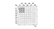
- 1st embodiment The top view of an electrostatic capacitance type sensor is shown, and the electrode pair group of an electrostatic capacitance type sensor at the time of measuring by an electrostatic capacitance measurement part by hatching is shown.
- the top view of an electrostatic capacitance type sensor is shown, and the electrode pair group of an electrostatic capacitance type sensor at the time of measuring by an electrostatic capacitance measurement part in the next measurement order of FIG. 3A by hatching is shown.
- the top view of an electrostatic capacitance type sensor is shown, and the electrode pair group of an electrostatic capacitance type sensor at the time of measuring by an electrostatic capacitance measurement part in the next measurement order of FIG. 3B by hatching is shown.
- the top view of an electrostatic capacitance type sensor is shown, and the electrode pair group of an electrostatic capacitance type sensor at the time of measuring by an electrostatic capacitance measurement part in the next measurement order of FIG. 3C by hatching is shown.
- 2nd embodiment The top view of a capacitive sensor is shown, and the electrode pair group of a capacitive sensor at the time of measuring by a capacitance measuring part by hatching is shown.
- the top view of an electrostatic capacitance type sensor is shown, and the electrode pair group of an electrostatic capacitance type sensor at the time of measuring by an electrostatic capacitance measurement part in the next measurement order of FIG.
- the top view of an electrostatic capacitance type sensor is shown, and the electrode pair group of an electrostatic capacitance type sensor at the time of measuring by an electrostatic capacitance measurement part in the next measurement order of FIG. 4B by hatching is shown.
- the top view of an electrostatic capacitance type sensor is shown, and the electrode pair group of an electrostatic capacitance type sensor at the time of measuring by an electrostatic capacitance measurement part in the next measurement order of FIG. 4C by hatching is shown.
- the top view of an electrostatic capacitance type sensor is shown, and the electrode pair group of an electrostatic capacitance type sensor at the time of measuring by an electrostatic capacitance measurement part in the next measurement order of FIG. 4D by hatching is shown.
- the top view of an electrostatic capacitance type sensor is shown, and the electrode pair group of an electrostatic capacitance type sensor at the time of measuring by an electrostatic capacitance measurement part in the next measurement order of FIG. 4E by hatching is shown.
- 3rd embodiment The top view of an electrostatic capacitance type sensor is shown, and the electrode pair group of an electrostatic capacitance type sensor at the time of measuring by an electrostatic capacitance measurement part by hatching is shown.
- the capacitive sensor device of the first embodiment will be described with reference to FIGS. 1 and 2.
- the capacitive sensor device can detect the distribution of the external force applied to the surface of the capacitive sensor formed in a sheet shape, that is, the position and magnitude of the external force.
- the capacitive sensor device will be described in detail below.
- the capacitance type sensor device includes a capacitance type sensor 10, an AC power supply 20, an input side switching circuit 30, an output side switching circuit 40, a capacitance measuring unit 50, and an external force calculating unit 60.
- the capacitance type sensor 10 is formed in a sheet shape, and has flexibility and a stretchable property. Therefore, the capacitive sensor 10 can be formed not only in a planar shape but also in a curved shape. However, the planar capacitive sensor 10 will be described below with reference to FIG.
- the capacitance type sensor 10 includes an electrode pair Es (configured by first and second electrodes 11a to 11i and 12a to 12i) provided to face each other with a distance in the surface normal direction (vertical direction in FIG. 1). Are arranged in a matrix, and an elastically deformable dielectric layer 13 is disposed between the electrode pair Es.
- a capacitive sensor in which electrode pairs Es are arranged in a matrix of 9 rows in the horizontal direction (hereinafter “X direction”) and 9 rows in the vertical direction (hereinafter “Y direction”). 10 is shown.
- X direction 9 rows in the horizontal direction
- Y direction 9 rows in the vertical direction
- the capacitance type sensor 10 is configured as follows because the number of electrodes and the number of wirings increase when the electrode pairs Es are scattered in a matrix. That is, the capacitive sensor 10 includes a first electrode group 11, a second electrode group 12, a dielectric layer 13 provided between the first and second electrode groups 11, 12, and the second electrode group 12 side. Insulating layers 14 and 15 are provided so as to cover the front surface and the back surface on the first electrode group 11 side.
- the first electrode group 11 has a plurality (for example, 9 rows) of long plate-shaped first electrodes 11a to 11i extending in the X direction parallel to the Y direction (direction orthogonal to the X axis direction).
- the second electrode group 12 includes a plurality of (e.g., nine rows) long plate-shaped second electrodes 12 a to 12 i extending in the Y direction, and arranged in parallel to the X direction. Are arranged opposite to each other at a distance.
- the second electrode group 12 is arranged on the surface side of the capacitive sensor 10 with respect to the first electrode group 11.
- each of the parts where the first electrode group 11 and the second electrode group 12 intersect constitute an electrode pair Es.
- the separation distance between the first electrodes 11a to 11i and the second electrodes 12a to 12i changes according to the external force F applied to the surface of the capacitive sensor 10, and the first electrodes 11a to 11a change with this change.
- the capacitance between 11i and the second electrodes 12a to 12i changes. Since it is well known that the capacitance is inversely proportional to the distance between the electrodes, detailed description is omitted.
- the first and second electrodes 11a to 11i and 12a to 12i are made of the same material. Specifically, the materials of the first and second electrodes 11a to 11i and 12a to 12i are formed by blending a conductive filler in an elastomer. The first and second electrodes 11a to 11i and 12a to 12i are flexible and stretchable.
- Examples of the elastomer constituting the first and second electrodes 11a to 11i and 12a to 12i include silicone rubber, ethylene-propylene copolymer rubber, natural rubber, styrene-butadiene copolymer rubber, acrylonitrile-butadiene copolymer rubber, and acrylic rubber. Epichlorohydrin rubber, chlorosulfonated polyethylene, chlorinated polyethylene, urethane rubber and the like can be applied. Further, the conductive filler blended in the first and second electrodes 11a to 11i and 12a to 12i may be any conductive particles, and for example, fine particles such as carbon materials and metals can be applied.
- the dielectric layer 13 is formed of an elastomer or a resin, and has flexibility and a stretchable property, like the first and second electrodes 11a to 11i and 12a to 12i.
- the elastomer constituting the dielectric layer 13 include silicone rubber, acrylonitrile-butadiene copolymer rubber, acrylic rubber, epichlorohydrin rubber, chlorosulfonated polyethylene, chlorinated polyethylene, and urethane rubber.
- the resin constituting the dielectric layer 13 for example, polyethylene, polypropylene, polyurethane, polystyrene (including cross-linked expanded polystyrene), polyvinyl chloride-polyvinylidene chloride copolymer, ethylene-acetic acid copolymer, and the like can be applied.
- the dielectric layer 13 has a set thickness and is formed to be approximately the same as or larger than the outer shape of the first and second electrode groups 11 and 12.
- the insulating layers 14 and 15 are flexible and extendable and contractible, like the first and second electrodes 11a to 11i and 12a to 12i.
- the elastomer or resin constituting the insulating layers 14 and 15 for example, materials described as the elastomer or resin constituting the dielectric layer 13 are applied.
- the dielectric layer 13 compresses and deforms in the surface normal direction, so that the external force F
- the separation distance between the first and second electrodes 11a to 11i and 12a to 12i located at the site to which is given is shortened. In this case, the capacitance between the first and second electrodes 11a to 11i and 12a to 12i is increased.
- the AC power supply 20 generates an AC voltage and applies it to the first electrode group 11 of the capacitive sensor 10.
- the input side switching circuit 30 includes a plurality of switches 30a to 30i. One end of each switch 30a to 30i is connected to the AC power supply 20, and the other end of each switch 30a to 30i is connected to the corresponding first electrode 11a to 11i. Then, a plurality selected from the first electrodes 11a to 11i are connected to the AC power supply 20, and the remaining first electrodes 11a to 11i are disconnected from the AC power supply. In FIG. 2, the first and second switches 30a and 30b of the input side switching circuit 30 are short-circuited (ON) and the other switches 30c to 30i are disconnected (OFF).
- the output side switching circuit 40 includes a plurality of switches 40a to 40i. One end of each switch 40a to 40i is connected to the corresponding second electrode 12a to 12i, and the other end of each switch 40a to 40i is connected to the capacitance measuring unit 50. Then, a plurality selected from the second electrodes 12a to 12i and the capacitance measuring unit 50 are connected, and the remaining second electrodes 12a to 12i are disconnected. In FIG. 2, the first and second switches 40a and 40b of the output side switching circuit 40 are short-circuited (ON) and the other switches 40c to 40i are disconnected (OFF).
- the capacitance measuring unit 50 includes a first electrode 11a to 11i to which an alternating voltage is applied in the first electrode group 11 and a second electrode 12a connected to the second electrode group 12 by the output side switching circuit 40. Measure the capacitance between ⁇ 12i. However, actually, the capacitance measuring unit 50 measures a voltage according to the capacitance.
- FIG. 2 shows a state in which the capacitance measuring unit 50 measures a voltage corresponding to the capacitance between the first electrodes 11a and 11b and the second electrodes 12a and 12b.
- the electrode pair Es is represented by a broken-line square. That is, the electrode pair Es corresponds to a portion where the first electrodes 11a to 11i and the second electrodes 12a to 12i shown in FIG. 2 intersect.
- the capacitance measuring unit 50 measures the capacitance of the electrode pair group Eg in the hatched range (X1 to X2, Y1 to Y2) of FIG. 3A.
- the first and second switches 30a and 30b of the input side switching circuit 30 are turned on, and the remaining switches 30c to 30i are turned off.
- the first and second switches 40a and 40b of the output side switching circuit 40 are turned on, and the remaining switches 40c to 40i are turned off.
- the capacitance of the electrode pair group Eg in the hatched range (X1 to X2, Y2 to Y3) in FIG. 3B is measured.
- the second and third switches 30b and 30c of the input side switching circuit 30 are turned on, and the remaining switches 30a and 30d to 30i are turned off. Further, the first and second switches 40a and 40b of the output side switching circuit 40 are turned on, and the remaining switches 40c to 40i are turned off.
- the capacitance of the electrode pair group Eg in the hatched range (X2 to X3, Y1 to Y2) in FIG. 3C is measured.
- the first and second switches 30a and 30b of the input side switching circuit 30 are turned on, and the remaining switches 30c to 30i are turned off.
- the second and third switches 40b and 40c of the output side switching circuit 40 are turned on, and the remaining switches 40a and 40d to 40i are turned off.
- the capacitance of the electrode pair group Eg in the hatched range (X2 to X3, Y2 to Y3) in FIG. 3D is measured.
- the second and third switches 30b and 30c of the input side switching circuit 30 are turned on, and the remaining switches 30a and 30d to 30i are turned off. Further, the second and third switches 40b and 40c of the output side switching circuit 40 are turned on, and the remaining switches 40a and 40d to 40i are turned off.
- the electrode pair group Eg simultaneously measured by the capacitance measuring unit 50 is set to four electrode pairs Es having a continuous square shape. Then, the capacitance measuring unit 50 measures the capacitance for all selectable electrode pair groups Eg from the matrix electrode pairs Es. For example, it is assumed that the selected electrode pair Es is the electrode pair Es at the coordinates (X2, Y2) in FIGS. 3A to 3D. In this case, as shown in FIGS. 3A to 3D, four types of electrode pair groups Eg (X1 to X2, Y1 to Y2), (X1 to X2, Y2) including the selected electrode pair Es (X2, Y2). To Y3), (X2 to X3, Y1 to Y2), and (X2 to X3, Y2 to Y3) are measured for capacitance.
- the external force calculation unit 60 shown in FIG. 1 and FIG. 2 is based on the capacitance of the plurality of electrode pair groups Eg measured by the capacitance measurement unit 50, and is applied to each electrode pair Es. The size of is calculated. A case where the external force at the electrode pair Es at the coordinates (X2, Y2) in FIGS. 3A to 3D is calculated will be described.
- Electrode pair groups Eg (X1 to X2, Y1 to Y2), (X1 to X2, Y2 to Y3), (X2 to X3, Y1 to Y2), (X2 to X3, Y2) measured by the capacitance measuring unit 50 each capacitance of ⁇ Y3), and C 12,12 + C 12,23 + C 23,12 + C 23,23.
- the electrode pair group Eg is set to four electrode pairs Es having four continuous square shapes. Therefore, the degree of influence of the measurement target coordinate (X2, Y2) on each electrode pair group Eg by the electrode pair Es is equal. Therefore, the capacitance C 22 of the electrode pair Es at the coordinates (X2, Y2) is measured as shown in Expression (1).
- the capacitance C 22 of the electrode pair Es at the calculated coordinates (X2, Y2) is a value corresponding to the magnitude of the external force applied to the electrode pair Es at the coordinates (X2, Y2). Therefore, the magnitude of the external force applied to the electrode pair Es at the coordinates (X2, Y2) can be calculated by setting the relationship between the magnitude of the capacitance and the magnitude of the external force in advance.
- the above formula (1) shows the capacitance C 22 of the electrode pair Es at the coordinates (X2, Y2).
- the electrostatic capacity C km of the electrode pair Es at other coordinates is expressed as in Expression (2).
- the electrostatic capacitance measurement part 50 does not measure the electrostatic capacitance for every electrode pair Es, but measures the electrostatic capacitance of the electrode pair group Eg comprised from several electrode pair Es. Accordingly, the area of the electrode pair at the time of measurement is not the area of one electrode pair Es but the area of a plurality of electrode pairs Es. Here, the capacitance increases as the area of the electrode pair increases. Therefore, by measuring the capacitance of the electrode pair group Eg, the measured capacitance outputs a larger value than when measuring the capacitance of one electrode pair Es. Therefore, the measured capacitance is highly accurate.
- the capacitance measuring unit 50 measures the capacitance of a plurality of combinations of the electrode pair group Eg including the selected electrode pair Es. That is, the selected electrode pair Es is included in an electrode pair group Eg composed of a plurality of combinations. Therefore, the capacitances of these electrode pair groups Eg are all values affected by the capacitance of the selected electrode pair Es.
- the magnitude of the external force F applied to the position of the selected electrode pair Es is calculated based on the capacitance of the electrode pair group Eg composed of a plurality of combinations.
- the capacitance of the selected electrode pair Es is proportional to the magnitude of the external force F applied to the selected electrode pair Es. Therefore, the external force calculation unit 60 calculates the external force F as a value proportional to the capacitance of the selected electrode pair Es using the capacitances of the plurality of electrode pair groups Eg. For example, in consideration of the influence degree of the selected electrode pair Es in the electrode pair group Eg, the influence degree of the capacitance of each electrode pair group Eg is determined and given to the selected electrode pair Es. The magnitude of the applied external force F is calculated. Therefore, it is possible to detect the external force F received by each electrode pair Es that constitutes the electrode pair group Eg. That is, the magnitude and position of the external force F applied to the matrix-type capacitive sensor can be obtained with high accuracy and high resolution.
- the electrode pair group Eg for measuring the capacitance in the capacitance measuring unit 50 is made up of a plurality of continuous electrode pairs Es.
- the influence degree of the selected electrode pair Es in the electrode pair group Eg can be determined relatively easily. In the above, it was equally divided. That is, it can be obtained with high accuracy by simple calculation.
- the electrode pair group Eg measured by the capacitance measuring unit 50 is (X1 to X2, Y1 to Y2) ⁇ (X1 to X2, Y2 to Y3) ⁇ (X2 to X3, Y1 to Y2).
- the description was made in the order of (X2 to X3, Y2 to Y3).
- the capacitance may be measured in the order shown in FIGS. 4A to 4F.
- the capacitance measuring unit 50 (shown in FIGS. 1 and 2) has the coordinates (X1 to X2, Y1 to Y2) of the electrode pair group Eg ⁇ (X1 to X2, Y3 to Y4) ⁇ (X1 to X2, Y5).
- ⁇ (X1 to X2, Y7 to Y8) ⁇ (X1 to X2, Y2 to Y3) ⁇ (X1 to X2, Y4 to Y5) in this order.
- the capacitance is measured in the order of (X1 to X2, Y6 to Y7) ⁇ (X1 to X2, Y8 to Y9), and then the X coordinate of the above electrode pair group is set to (X2 to X3). The capacitance is measured for the electrode pair group.
- the electrode pair group Eg measured by the capacitance measuring unit 50 is an electrode pair group Eg that does not include the electrode pair Es constituting the electrode pair group Eg measured immediately before.
- the electrode pair group Eg is charged by the capacitance measurement. If the electrode pair group Eg measured immediately before and the electrode pair group Eg measured this time overlap, the capacitance of the electrode pair group Eg charged by the previous measurement is added to the capacitance of the electrode pair group Eg measured this time. May be affected. Therefore, as described above, the electrode pair group Eg measured immediately before is not overlapped with the electrode pair group Eg measured this time. Therefore, the capacitance of the electrode pair group Eg measured this time is determined by the previous measurement. The influence of the electric charge charged on the group Eg can be reduced. As a result, the capacitance of the electrode pair group Eg measured this time can be measured with high accuracy. As a result, the position and magnitude of the external force F applied to the capacitive sensor 10 can be calculated with high accuracy.
- the electrode pair group Eg has been described as four square electrode pairs Es.
- the electrode pair group Eg may be nine square electrode pairs Es, or may be configured by an arbitrary plurality of electrode pairs Es.
- the external force calculation unit 60 calculates the coefficient for each electrode pair group Eg, The coefficient is set according to the degree of influence of the electrode pair Es to be calculated.
- the calculated capacitance of the electrode pair Es is calculated according to Equation (3).
- the first term on the right side of Equation (3) is the capacitance when the center coordinates of the nine electrode pairs coincide with the electrode pair Es to be calculated, and the second term on the right side is the center coordinates of the nine electrode pairs.
- the capacitance at a position shifted by one in the left-right or up-down direction of the electrode pair Es desired, and the third term on the right side is the capacitance when the corners of the nine electrode pairs coincide with the electrode pairs Es to be calculated.
- the coefficients a, b, and c are not limited to the following, and can be adjusted as appropriate.
Landscapes
- Engineering & Computer Science (AREA)
- Power Engineering (AREA)
- Physics & Mathematics (AREA)
- General Physics & Mathematics (AREA)
- Force Measurement Appropriate To Specific Purposes (AREA)
- Measurement Of Length, Angles, Or The Like Using Electric Or Magnetic Means (AREA)
Abstract
外力の位置および大きさを高精度に検出することができる静電容量型センサ装置を提供する。 距離を隔てて対向して設けられた電極対をマトリックス状に配置し、電極対の間に弾性変形可能な誘電層を配置してなる静電容量型センサを用いる。静電容量計測部が、選択された電極対を含む複数の電極対からなる電極対群の間の静電容量の計測を、複数の組み合わせからなる電極対群について行う。このようにして計測された複数の静電容量に基づいて、外力算出部が、選択された電極対の位置に付与された外力の大きさを算出する。
Description
本発明は、対向する電極対の間に弾性変形可能な誘電層を介在して形成された静電容量型センサに外力が付与された場合に、当該誘電層の変形に伴って変化する静電容量を計測することにより、当該外力の位置および大きさを計測することができる静電容量型センサ装置に関するものである。
静電容量を用いたタッチセンサが国際公開2009/013965号に記載されている。このタッチセンサは、配列された電極とアースとの間の静電容量を検出する。例えば、人間の指を接近させることで、接近した電極とアースとの静電容量が変化することを利用して、接近した指の位置を検出することとしている。
また、電極とアースとの間の静電容量を計測する装置ではなく、電極対をマトリックス状に配置し、外力の付与によって誘電層が弾性変形することにより当該電極対の間の距離が変化する静電容量型センサを対象とし、電極対間の静電容量を計測することで付与された外力の分布を計測する装置が、特公平6-52206号公報に記載されている。
特公平6-52206号公報に記載されている誘電層が弾性変形することにより電極対の間の距離が変化する装置においては、誘電層は、外力を受けたときに弾性変形することができる程度に厚みを有する必要がある。誘電層の厚みを確保すると、電極対の離間距離が大きくなる。電極対の離間距離が大きくなると、外力が付与されて誘電層が弾性変形した場合に、電極対の離間距離が小さくなることに伴って電極対の間の静電容量が変化するが、その静電容量の変化が小さい。そのため、検出できる外力の大きさの分解能が低くなり、外力の大きさを高精度に検出することができない。
そのことを解決するために、それぞれの電極対の面積を大きくすることで、同一の外力が付与された場合に静電容量の変化を大きくすることができる。しかしながら、それぞれの電極対の面積を大きくすると、同一の電極対内において、外力が付与された位置を検出することができない。つまり、センサ全体として見た場合に、外力の位置を高精度に検出することができないという問題を有する。このように、従来は、外力の位置を高精度に検出しつつ、外力の大きさを高精度に検出することは容易ではない。
本発明は、このような事情に鑑みてなされたものであり、外力の位置および大きさを高精度に検出することができる静電容量型センサ装置を提供することを目的とする。
本手段に係る静電容量型センサ装置は、距離を隔てて対向して設けられた電極対をマトリックス状に配置し、前記電極対の間に弾性変形可能な誘電層を配置してなる静電容量型センサと、選択された前記電極対を含む複数の前記電極対からなる電極対群の間の静電容量の計測を、複数の組み合わせからなる前記電極対群について行う静電容量計測部と、計測された複数の前記静電容量に基づいて、前記選択された前記電極対の位置に付与された外力の大きさを算出する外力算出部とを備える。
本手段によれば、外力により誘電層が弾性変形することに伴って電極対の離間距離が変化することで、電極対の間の静電容量が変化する。このことを利用して、外力の位置および大きさを取得している。そして、本手段における静電容量計測部は、それぞれの電極対ごとの静電容量を計測するのではなく、複数の電極対から構成される電極対群の静電容量を計測している。従って、計測する際の電極対の面積が、1つの電極対の面積ではなく、複数の電極対の面積となる。ここで、静電容量は、電極対の面積が大きいほど、大きな値となる。従って、電極対群の静電容量を計測することで、計測される静電容量は、1つの電極対の静電容量を計測する場合に比べて、大きな値を出力する。従って、計測される静電容量は、高精度となる。
しかし、単に、複数の電極対から構成される電極対群の静電容量を計測するのでは、従来のように、電極対の面積を大きくしたことに相当する。つまり、このままでは、電極対群の中で、外力が付与された位置を検出することができない。しかし、本手段によれば、以下により、電極対群の中で、外力が付与された位置を検出することができるようにしている。
本手段によれば、選択された電極対を含む電極対群の複数の組み合わせについて静電容量を計測する。つまり、選択された電極対は、複数の組合せからなる電極対群に含まれている。従って、これらの電極対群の静電容量は、全て、当該選択された電極対の静電容量の影響を受けた値となる。
そして、複数の組合せからなる電極対群の静電容量に基づいて、選択された電極対の位置に付与された外力の大きさを算出している。ここで、選択された電極対の静電容量は、当該選択された電極対に付与された外力の大きさに比例する。そこで、外力算出部は、複数の電極対群の静電容量を用いて、当該選択された電極対の静電容量に比例する値としての外力を算出している。例えば、電極対群の中で当該選択された電極対の影響度を考慮して、それぞれの電極対群の静電容量の影響度を決定し、当該選択された電極対に付与された外力の大きさを算出する。従って、電極対群を構成するそれぞれの電極対が受ける外力を検出することができる。つまり、マトリックス状の静電容量型センサに付与される外力の大きさおよび位置を高精度で且つ高分解能で得ることができる。
また、前記静電容量型センサは、第一方向に延びる第一電極を前記第一方向に直交する第二方向に複数配列した第一電極群と、前記第二方向に延びる第二電極を第一方向に複数配列し、前記第一電極群に対して距離を隔てて対向して配置された第二電極群と、前記第一電極群と前記第二電極群との間に配置された前記誘電層とを備えるようにしてもよい。これにより、電極数および配線数を減らすことができる。
また、前記静電容量計測部において静電容量を計測する前記電極対群は、連続した複数の前記電極対からなるようにしてもよい。これにより、電極対群の中で当該選択された電極対の影響度を、比較的容易に決定できる。つまり、簡易的な計算で高精度に得ることができる。
また、前記静電容量計測部において計測する前記電極対群は、直前に計測した前記電極対群を構成する前記電極対を含まない前記電極対群であるとしてもよい。ここで、静電容量の計測により、電極対群は帯電する。そして、直前に計測した電極対群と今回計測する電極対群とが重なっていると、今回計測する電極対群の静電容量に、前回計測により電極対群に帯電した電荷の影響を受けるおそれがある。これに対して、上記によれば、直前に計測した電極対群と今回計測する電極対群とは、重なっていない。従って、今回計測する電極対群の静電容量は、前回計測により電極対群に帯電した電荷の影響を小さくできる。その結果、今回計測する電極対群の静電容量を高精度に計測することができる。ひいては、静電容量型センサに付与された外力の位置および大きさを高精度に算出することができる。
<第一実施形態>
第一実施形態の静電容量型センサ装置について、図1および図2を参照して説明する。静電容量型センサ装置は、シート状に形成された静電容量型センサの表面に付与された外力の分布、すなわち外力の位置および大きさを検出することができる。静電容量型センサ装置について以下に詳細に説明する。
第一実施形態の静電容量型センサ装置について、図1および図2を参照して説明する。静電容量型センサ装置は、シート状に形成された静電容量型センサの表面に付与された外力の分布、すなわち外力の位置および大きさを検出することができる。静電容量型センサ装置について以下に詳細に説明する。
静電容量型センサ装置は、静電容量型センサ10と、交流電源20と、入力側切換回路30と、出力側切換回路40と、静電容量計測部50と、外力算出部60とを備える。静電容量型センサ10は、シート状に形成されており、可撓性を有し且つ伸縮自在な性質を有する。従って、静電容量型センサ10は、平面形状のみならず、曲面形状に形成することもできる。ただし、以下において、図1を参照して、平面形状の静電容量型センサ10について説明する。
静電容量型センサ10は、面法線方向(図1の上下方向)に距離を隔てて対向して設けられた電極対Es(第一,第二電極11a~11i,12a~12iにより構成)をマトリックス状に配置し、電極対Esの間に弾性変形可能な誘電層13を配置している。図2においては、電極対Esを、横方向(以下、「X方向」)に9列、縦方向(以下、「Y方向」)に9列のマトリックス状に配置している静電容量型センサ10を示す。図2において、Aで囲む部位は、電極対Esの一つを示している。
ただし、静電容量型センサ10は、マトリックス状に電極対Esを点在させると、電極数および配線数が多くなるため、以下のように構成している。すなわち、静電容量型センサ10は、第一電極群11、第二電極群12と、第一,第二電極群11,12間に設けられた誘電層13と、第二電極群12側の表面および第一電極群11側の裏面を被覆するように設けられた絶縁層14,15を備えて構成される。
第一電極群11は、X方向に延びる長尺板形状の第一電極11a~11iをY方向(X軸方向に直交する方向)に平行に複数(例えば、9列)配列する。第二電極群12は、Y方向に延びる長尺板形状の第二電極12a~12iをX方向に平行に複数(例えば、9列)配列し、第一電極群11に対して面法線方向に距離を隔てて対向して配置される。ここでは、第二電極群12は、第一電極群11に対して静電容量型センサ10の表面側に配置される。ここで、第一電極群11と第二電極群12とが交差する部位のそれぞれが、電極対Esを構成する。
そして、静電容量型センサ10の表面に付与される外力Fに応じて第一電極11a~11iと第二電極12a~12iとの離間距離が変化し、この変化に伴って第一電極11a~11iと第二電極12a~12iの間の静電容量が変化する。なお、静電容量が電極間距離に反比例する関係にあることは周知であるため、詳細な説明は省略する。
第一,第二電極11a~11i,12a~12iは、同一材質により形成されている。具体的には、第一,第二電極11a~11i,12a~12iの材質は、エラストマー中に導電性フィラーを配合させることにより成形している。そして、第一,第二電極11a~11i,12a~12iは、可撓性を有し且つ伸縮自在な性質を有するようにしている。
第一,第二電極11a~11i,12a~12iを構成するエラストマーは、例えば、シリコーンゴム、エチレン-プロピレン共重合ゴム、天然ゴム、スチレン-ブタジエン共重合ゴム、アクリロニトリル-ブタジエン共重合ゴム、アクリルゴム、エピクロロヒドリンゴム、クロロスルホン化ポリエチレン、塩素化ポリエチレン、ウレタンゴムなどが適用できる。また、第一,第二電極11a~11i,12a~12iに配合される導電性フィラーは、導電性を有する粒子であればよく、例えば、炭素材料や金属等の微粒子を適用できる。
誘電層13は、エラストマーまたは樹脂により成形され、第一,第二電極11a~11i,12a~12iと同様に、可撓性を有し且つ伸縮自在な性質を有する。この誘電層13を構成するエラストマーは、例えば、シリコーンゴム、アクリロニトリル-ブタジエン共重合ゴム、アクリルゴム、エピクロロヒドリンゴム、クロロスルホン化ポリエチレン、塩素化ポリエチレン、ウレタンゴムなどが適用できる。また、誘電層13を構成する樹脂は、例えば、ポリエチレン、ポリプロピレン、ポリウレタン、ポリスチレン(架橋発泡ポリスチレンを含む)、ポリ塩化ビニル-ポリ塩化ビニリデン共重合体、エチレン-酢酸共重合体などが適用できる。
この誘電層13は、設定された厚みを有し、第一,第二電極群11,12の外形状と同程度または大きく形成されている。絶縁層14,15は、第一,第二電極11a~11i,12a~12iと同様に、可撓性を有し且つ伸縮自在な性質を有する。この絶縁層14,15を構成するエラストマーまたは樹脂は、例えば、誘電層13を構成するエラストマーまたは樹脂として記載した材料が適用される。
そして、静電容量型センサ10が静電容量型センサ10の面法線方向に圧縮する外力Fを受けた場合には、誘電層13が当該面法線方向に圧縮変形することにより、外力Fが付与された部位に位置する第一,第二電極11a~11i,12a~12i間の離間距離が短くなる。この場合、当該第一,第二電極11a~11i,12a~12i間の静電容量は大きくなる。
交流電源20は、交流電圧を発生し、静電容量型センサ10の第一電極群11に対して印加する。
入力側切換回路30は、複数のスイッチ30a~30iにより構成されている。各スイッチ30a~30iの一端は、交流電源20に接続されており、各スイッチ30a~30iの他端は、対応する第一電極11a~11iに接続されている。そして、第一電極11a~11iの中から選択された複数と交流電源20とを接続し、第一電極11a~11iの残りは交流電源に対して切断する。なお、図2においては、入力側切換回路30の第一,第二スイッチ30a,30bを短絡(ON)させ、他のスイッチ30c~30iを切断(OFF)している。
出力側切換回路40は、複数のスイッチ40a~40iにより構成されている。各スイッチ40a~40iの一端は、対応する第二電極12a~12iに接続され、各スイッチ40a~40iの他端は、静電容量計測部50に接続される。そして、第二電極12a~12iの中から選択された複数と静電容量計測部50とを接続し、第二電極12a~12iの残りを切断する。なお、図2においては、出力側切換回路40の第一,第二スイッチ40a,40bを短絡(ON)させ、他のスイッチ40c~40iを切断(OFF)している。
静電容量計測部50は、第一電極群11のうち交流電圧が印加されている第一電極11a~11iと第二電極群12のうち出力側切換回路40により接続されている第二電極12a~12iとの間の静電容量を計測する。ただし、実際には、静電容量計測部50は、当該静電容量に応じた電圧を計測する。ここで、図2には、静電容量計測部50は、第一電極11a,11bと第二電極12a,12bとの間の静電容量に応じた電圧を計測する状態を示している。
ここで、図3A~図3Dを参照して、静電容量計測部50による静電容量を計測する手順について説明する。ここで、図3A~図3Dにおいて、電極対Esを破線の正方形にて表している。つまり、当該電極対Esは、図2に示す第一電極11a~11iと第二電極12a~12iとが交差する部位に対応している。
最初に、静電容量計測部50は、図3Aのハッチングの範囲(X1~X2,Y1~Y2)の電極対群Egの静電容量を計測する。このとき、入力側切換回路30の第一,第二スイッチ30a,30bがONされ、残りのスイッチ30c~30iはOFFされる。また、出力側切換回路40の第一,第二スイッチ40a,40bがONされ、残りのスイッチ40c~40iがOFFされる。続いて、図3Bのハッチングの範囲(X1~X2,Y2~Y3)の電極対群Egの静電容量を計測する。このとき、入力側切換回路30の第二,第三スイッチ30b,30cがONされ、残りのスイッチ30a,30d~30iはOFFされる。また、出力側切換回路40の第一,第二スイッチ40a,40bがONされ、残りのスイッチ40c~40iがOFFされる。
続いて、図3Cのハッチングの範囲(X2~X3,Y1~Y2)の電極対群Egの静電容量を計測する。このとき、入力側切換回路30の第一,第二スイッチ30a,30bがONされ、残りのスイッチ30c~30iはOFFされる。また、出力側切換回路40の第二,第三スイッチ40b,40cがONされ、残りのスイッチ40a,40d~40iがOFFされる。続いて、図3Dのハッチングの範囲(X2~X3,Y2~Y3)の電極対群Egの静電容量を計測する。このとき、入力側切換回路30の第二,第三スイッチ30b,30cがONされ、残りのスイッチ30a,30d~30iはOFFされる。また、出力側切換回路40の第二,第三スイッチ40b,40cがONされ、残りのスイッチ40a,40d~40iがOFFされる。
このように、静電容量計測部50により同時に計測する電極対群Egは、連続した正方形状となる4つの電極対Esとしている。そして、マトリックス状の電極対Esの中から、選択可能な全ての電極対群Egを対象として、静電容量計測部50が静電容量を計測する。例えば、選択された電極対Esを、図3A~図3Dの座標(X2,Y2)の電極対Esであるとする。この場合、図3A~図3Dに示すように、当該選択された電極対Es(X2,Y2)を含む4種類の電極対群Eg(X1~X2,Y1~Y2)、(X1~X2,Y2~Y3)、(X2~X3,Y1~Y2)、(X2~X3,Y2~Y3)についての静電容量を計測する。
図1および図2に示す外力算出部60は、静電容量計測部50により計測された複数の電極対群Egの静電容量に基づいて、それぞれの電極対Esに対して付与されている外力の大きさを算出する。図3A~図3Dにおける座標(X2,Y2)の電極対Esにおける外力を算出する場合について説明する。
静電容量計測部50により計測された電極対群Eg(X1~X2,Y1~Y2)、(X1~X2,Y2~Y3)、(X2~X3,Y1~Y2)、(X2~X3,Y2~Y3)の静電容量をそれぞれ、C12,12+C12,23+C23,12+C23,23とする。ここで、電極対群Egは、連続した4つの正方形状となる4つの電極対Esとしている。従って、計測対象の座標(X2,Y2)の電極対Esによるそれぞれの電極対群Egに対する影響度は、均等とする。そこで、式(1)に示すようにして、座標(X2,Y2)の電極対Esの静電容量C22を計測する。

算出した座標(X2,Y2)の電極対Esの静電容量C22は、座標(X2,Y2)の電極対Esに付与される外力の大きさに応じた値となる。そこで、予め静電容量の大きさと外力の大きさの関係を設定しておくことで、座標(X2,Y2)の電極対Esに付与される外力の大きさを算出できる。
ここで、上記式(1)は、座標(X2,Y2)の電極対Esの静電容量C22について示した。他の座標の電極対Esの静電容量Ckmについては、式(2)のように表される。

以上説明したように、外力Fにより誘電層13が弾性変形することに伴って電極対Esの離間距離が変化することで、電極対Esの間の静電容量が変化する。このことを利用して、外力Fの位置および大きさを取得している。そして、静電容量計測部50は、それぞれの電極対Esごとの静電容量を計測するのではなく、複数の電極対Esから構成される電極対群Egの静電容量を計測している。従って、計測する際の電極対の面積が、1つの電極対Esの面積ではなく、複数の電極対Esの面積となる。ここで、静電容量は、電極対の面積が大きいほど、大きな値となる。従って、電極対群Egの静電容量を計測することで、計測される静電容量は、1つの電極対Esの静電容量を計測する場合に比べて、大きな値を出力する。従って、計測される静電容量は、高精度となる。
しかし、単に、複数の電極対Esから構成される電極対群Egの静電容量を計測するのでは、従来のように、電極対Esの面積を大きくしたことに相当する。つまり、このままでは、電極対群Egの中で、外力Fが付与された位置を検出することができない。これに対して、静電容量計測部50は、選択された電極対Esを含む電極対群Egの複数の組み合わせについて静電容量を計測する。つまり、選択された電極対Esは、複数の組合せからなる電極対群Egに含まれている。従って、これらの電極対群Egの静電容量は、全て、当該選択された電極対Esの静電容量の影響を受けた値となる。
そして、複数の組合せからなる電極対群Egの静電容量に基づいて、選択された電極対Esの位置に付与された外力Fの大きさを算出している。ここで、選択された電極対Esの静電容量は、当該選択された電極対Esに付与された外力Fの大きさに比例する。そこで、外力算出部60は、複数の電極対群Egの静電容量を用いて、当該選択された電極対Esの静電容量に比例する値としての外力Fを算出している。例えば、電極対群Egの中で当該選択された電極対Esの影響度を考慮して、それぞれの電極対群Egの静電容量の影響度を決定し、当該選択された電極対Esに付与された外力Fの大きさを算出する。従って、電極対群Egを構成するそれぞれの電極対Esが受ける外力Fを検出することができる。つまり、マトリックス状の静電容量型センサに付与される外力Fの大きさおよび位置を高精度で且つ高分解能で得ることができる。
また、静電容量計測部50において静電容量を計測する電極対群Egは、連続した複数の電極対Esからなるようにしている。これにより、上述したように、電極対群Egの中で当該選択された電極対Esの影響度を、比較的容易に決定できる。上記においては、均等割とした。つまり、簡易的な計算で高精度に得ることができる。
<第二実施形態>
第一実施形態において、静電容量計測部50により計測する電極対群Egは、(X1~X2,Y1~Y2)→(X1~X2,Y2~Y3)→(X2~X3,Y1~Y2)→(X2~X3,Y2~Y3)の順として説明した。この他に、図4A~図4Fに示す順序で静電容量の計測を行っても良い。
第一実施形態において、静電容量計測部50により計測する電極対群Egは、(X1~X2,Y1~Y2)→(X1~X2,Y2~Y3)→(X2~X3,Y1~Y2)→(X2~X3,Y2~Y3)の順として説明した。この他に、図4A~図4Fに示す順序で静電容量の計測を行っても良い。
つまり、静電容量計測部50(図1,2に示す)は、電極対群Egの座標(X1~X2,Y1~Y2)→(X1~X2,Y3~Y4)→(X1~X2,Y5~Y6)→(X1~X2,Y7~Y8)→(X1~X2,Y2~Y3)→(X1~X2,Y4~Y5)の順に静電容量を計測する。この後は、例えば、(X1~X2,Y6~Y7)→(X1~X2,Y8~Y9)の順に静電容量を計測し、続いて、上記の電極対群のX座標を(X2~X3)とした電極対群について静電容量を計測する。
このように、静電容量計測部50において計測する電極対群Egは、直前に計測した電極対群Egを構成する電極対Esを含まない電極対群Egとしている。ここで、静電容量の計測により、電極対群Egは帯電する。そして、直前に計測した電極対群Egと今回計測する電極対群Egとが重なっていると、今回計測する電極対群Egの静電容量に、前回計測により電極対群Egに帯電した電荷の影響を受けるおそれがある。そこで、上述したように、直前に計測した電極対群Egと今回計測する電極対群Egとが重ならないようにする従って、今回計測する電極対群Egの静電容量は、前回計測により電極対群Egに帯電した電荷の影響を小さくできる。その結果、今回計測する電極対群Egの静電容量を高精度に計測することができる。ひいては、静電容量型センサ10に付与された外力Fの位置および大きさを高精度に算出することができる。
<第三実施形態>
また、上記第一,第二実施形態においては、電極対群Egを4つの正方形状の電極対Esとして説明した。電極対群Egは、例えば、図5に示すように、9つの正方形状の電極対Esとしてもよく、その他に、任意の複数の電極対Esにより構成することもできる。
また、上記第一,第二実施形態においては、電極対群Egを4つの正方形状の電極対Esとして説明した。電極対群Egは、例えば、図5に示すように、9つの正方形状の電極対Esとしてもよく、その他に、任意の複数の電極対Esにより構成することもできる。
図5に示すような9つの正方形状の電極対Esにより電極対群Egを構成する場合には、外力算出部60(図1,2に示す)は、それぞれの電極対群Egに対する係数を、算出したい電極対Esの影響度に応じた係数に設定する。例えば、式(3)に従って、算出した電極対Esの静電容量を算出する。式(3)の右辺第一項は、9つの電極対の中心座標が算出したい電極対Esに一致する場合の静電容量であり、右辺第二項は、9つの電極対の中心座標が算出したい電極対Esの左右または上下に1つずれた位置における静電容量であり、右辺第三項は、9つの電極対の角部が算出したい電極対Esに一致する場合の静電容量である。なお、係数a,b,cは、以下に限られず、適宜調整することができる。

10:静電容量型センサ、 11:第一電極群、 11a~11i:第一電極、 12:第二電極群、 12a~12i:第二電極、 13:誘電層、 14,15:絶縁層、 50:静電容量計測部、 60:外力算出部、 Es:電極対、 Eg:電極対群、 F:外力
Claims (4)
- 距離を隔てて対向して設けられた電極対をマトリックス状に配置し、前記電極対の間に弾性変形可能な誘電層を配置してなる静電容量型センサと、
選択された前記電極対を含む複数の前記電極対からなる電極対群の間の静電容量の計測を、複数の組み合わせからなる前記電極対群について行う静電容量計測部と、
計測された複数の前記静電容量に基づいて、前記選択された前記電極対の位置に付与された外力の大きさを算出する外力算出部と、
を備える、静電容量型センサ装置。 - 前記静電容量型センサは、
第一方向に延びる第一電極を前記第一方向に直交する第二方向に複数配列した第一電極群と、
前記第二方向に延びる第二電極を第一方向に複数配列し、前記第一電極群に対して距離を隔てて対向して配置された第二電極群と、
前記第一電極群と前記第二電極群との間に配置された前記誘電層と、
を備える、請求項1の静電容量型センサ装置。 - 前記静電容量計測部において静電容量を計測する前記電極対群は、連続した複数の前記電極対からなる、請求項1の静電容量型センサ装置。
- 前記静電容量計測部において計測する前記電極対群は、直前に計測した前記電極対群を構成する前記電極対を含まない前記電極対群である、請求項1の静電容量型センサ装置。
Priority Applications (3)
| Application Number | Priority Date | Filing Date | Title |
|---|---|---|---|
| EP12773658.5A EP2573533B1 (en) | 2011-04-19 | 2012-04-19 | Capacitive sensor device |
| CN201280002657.0A CN103080714B (zh) | 2011-04-19 | 2012-04-19 | 静电电容式传感器装置 |
| US13/686,325 US9525417B2 (en) | 2011-04-19 | 2012-11-27 | Capacitive sensor device |
Applications Claiming Priority (2)
| Application Number | Priority Date | Filing Date | Title |
|---|---|---|---|
| JP2011-092712 | 2011-04-19 | ||
| JP2011092712A JP5432207B2 (ja) | 2011-04-19 | 2011-04-19 | 静電容量型センサ装置 |
Related Child Applications (1)
| Application Number | Title | Priority Date | Filing Date |
|---|---|---|---|
| US13/686,325 Continuation US9525417B2 (en) | 2011-04-19 | 2012-11-27 | Capacitive sensor device |
Publications (1)
| Publication Number | Publication Date |
|---|---|
| WO2012144550A1 true WO2012144550A1 (ja) | 2012-10-26 |
Family
ID=47041656
Family Applications (1)
| Application Number | Title | Priority Date | Filing Date |
|---|---|---|---|
| PCT/JP2012/060551 Ceased WO2012144550A1 (ja) | 2011-04-19 | 2012-04-19 | 静電容量型センサ装置 |
Country Status (5)
| Country | Link |
|---|---|
| US (1) | US9525417B2 (ja) |
| EP (1) | EP2573533B1 (ja) |
| JP (1) | JP5432207B2 (ja) |
| CN (1) | CN103080714B (ja) |
| WO (1) | WO2012144550A1 (ja) |
Families Citing this family (38)
| Publication number | Priority date | Publication date | Assignee | Title |
|---|---|---|---|---|
| JP6030841B2 (ja) | 2012-03-26 | 2016-11-24 | 住友理工株式会社 | 静電容量型センサ |
| JP5497222B2 (ja) * | 2012-09-28 | 2014-05-21 | バンドー化学株式会社 | 静電容量型センサシート及び静電容量型センサシートの製造方法 |
| WO2014157627A1 (ja) | 2013-03-29 | 2014-10-02 | バンドー化学株式会社 | 静電容量型センサシート及び静電容量型センサ |
| US10955973B2 (en) * | 2013-04-16 | 2021-03-23 | Atmel Corporation | Differential sensing for touch sensors |
| JP2014219214A (ja) * | 2013-05-01 | 2014-11-20 | バンドー化学株式会社 | 静電容量型センサシート及び静電容量型センサ |
| JP2014219263A (ja) * | 2013-05-08 | 2014-11-20 | バンドー化学株式会社 | 静電容量型センサシート及び静電容量型センサ |
| JP2015045623A (ja) * | 2013-08-29 | 2015-03-12 | バンドー化学株式会社 | 静電容量型センサシート及び静電容量型センサ |
| JP6167863B2 (ja) * | 2013-11-08 | 2017-07-26 | 東洋インキScホールディングス株式会社 | 形状測定装置 |
| EP3076402B1 (en) * | 2013-11-28 | 2022-06-08 | Bando Chemical Industries, Ltd. | Stretchable electrode, sensor sheet and capacitive sensor |
| CN104720913B (zh) | 2013-12-19 | 2017-07-18 | 高露洁-棕榄公司 | 电动牙刷 |
| CN104720914B (zh) * | 2013-12-19 | 2017-10-03 | 高露洁-棕榄公司 | 电动牙刷 |
| JP6325289B2 (ja) * | 2014-03-06 | 2018-05-16 | 国立大学法人信州大学 | シートセンサシステムおよびシートセンサ |
| US9417729B2 (en) * | 2014-06-09 | 2016-08-16 | Atmel Corporation | Charge compensation during touch sensing |
| KR102245943B1 (ko) | 2014-06-23 | 2021-04-29 | 엘지디스플레이 주식회사 | 터치 패널 및 이의 구동 장치 |
| KR20160041487A (ko) * | 2014-10-08 | 2016-04-18 | 삼성전자주식회사 | 터치 패널 및 그를 가지는 디스플레이 장치 |
| CN107209586A (zh) | 2014-11-05 | 2017-09-26 | 3M创新有限公司 | 力感测电容器元件、可变形膜以及由其制造的电子设备 |
| DE102014016772A1 (de) * | 2014-11-13 | 2016-05-19 | Audi Ag | Eingabevorrichtung für einen Kraftwagen, Kraftwagen mit einer Eingabevorrichtung und Verfahren zum Betreiben einer Eingabevorrichtung |
| CN105067160B (zh) * | 2015-07-23 | 2017-10-03 | 东南大学 | 基于氧化石墨烯海绵的柔性压力传感器 |
| WO2017022258A1 (ja) * | 2015-07-31 | 2017-02-09 | 住友理工株式会社 | 静電容量型センサ、センサシートおよび静電容量型センサの製造方法 |
| CN105387957B (zh) * | 2015-10-16 | 2018-05-04 | 北京印刷学院 | 基于印刷透明电极的可拉伸压力传感器及其制备方法 |
| US9802316B2 (en) * | 2016-01-15 | 2017-10-31 | Vision Robotics Corporation | Compliant touch sensor |
| US10725576B2 (en) * | 2016-03-31 | 2020-07-28 | Japan Display Inc. | Detection device, display device, and detection method |
| JP2017188106A (ja) * | 2016-03-31 | 2017-10-12 | 株式会社ジャパンディスプレイ | 検出装置、表示装置及び検出方法 |
| JP6557628B2 (ja) * | 2016-03-31 | 2019-08-07 | 株式会社ジャパンディスプレイ | 検出装置、表示装置及び検出方法 |
| CN109661558A (zh) | 2016-09-06 | 2019-04-19 | 积水化学工业株式会社 | 压电传感器 |
| KR102616363B1 (ko) * | 2016-09-30 | 2023-12-27 | 엘지디스플레이 주식회사 | 구동 방법, 터치 센싱 회로 및 터치 표시 장치 |
| JP6773528B2 (ja) * | 2016-11-15 | 2020-10-21 | 株式会社ジャパンディスプレイ | 感圧センサ及び感圧センサ付表示装置 |
| JP6642474B2 (ja) * | 2017-02-13 | 2020-02-05 | オムロン株式会社 | 状態判定装置、学習装置、状態判定方法及びプログラム |
| JP2018155713A (ja) * | 2017-03-21 | 2018-10-04 | 住友理工株式会社 | センサ装置 |
| TWI791491B (zh) * | 2018-03-02 | 2023-02-11 | 日商積水化學工業股份有限公司 | 壓電感測器 |
| JP2018091875A (ja) * | 2018-03-22 | 2018-06-14 | バンドー化学株式会社 | シート状物、静電容量型センサシート、及び、衣服 |
| CN108534921B (zh) * | 2018-03-26 | 2021-01-26 | 京东方科技集团股份有限公司 | 压力传感器、显示装置 |
| KR102051215B1 (ko) * | 2018-04-16 | 2019-12-02 | 최정태 | 정전용량 압력검출방식의 매트형 센싱 장치 및 그의 제작 방법 |
| US10622996B1 (en) | 2019-03-29 | 2020-04-14 | Industrial Technology Research Institute | Adjustable sensing capacitance microelectromechanical system (MEMS) apparatus |
| TWI705235B (zh) | 2019-07-19 | 2020-09-21 | 財團法人工業技術研究院 | 感測裝置 |
| JP7521263B2 (ja) * | 2020-06-01 | 2024-07-24 | Toppanホールディングス株式会社 | 圧力センサー及び大型圧力センサー |
| DE112021003067T5 (de) | 2020-06-02 | 2023-03-16 | Microchip Technology Incorporated | Kapazitive sensorik unter verwendung einer differenzwertangabe |
| DE112023004687T5 (de) * | 2022-11-10 | 2025-09-04 | Alps Alpine Co., Ltd. | Eingabevorrichtung |
Citations (7)
| Publication number | Priority date | Publication date | Assignee | Title |
|---|---|---|---|---|
| JPS6052206B2 (ja) | 1978-03-27 | 1985-11-18 | 三菱レイヨン株式会社 | アクリル系炭素繊維の製造方法 |
| JPH01214727A (ja) * | 1988-02-24 | 1989-08-29 | Anima Kk | 圧力分布測定装置 |
| JP2001287189A (ja) * | 2000-04-10 | 2001-10-16 | Natl Aerospace Lab | 多関節介護ロボット制御用の圧力分布センサ |
| JP2003014564A (ja) * | 2001-06-28 | 2003-01-15 | Fujitsu Ten Ltd | シートセンサ、及び乗員検知システム |
| JP2006329909A (ja) * | 2005-05-30 | 2006-12-07 | Toyota Motor Corp | 圧力分布センサ |
| WO2009013965A1 (ja) | 2007-07-20 | 2009-01-29 | Japan Aviation Electronics Industry Limited | 静電容量センサ、位置センサ |
| JP2009058445A (ja) * | 2007-08-31 | 2009-03-19 | Niigata Univ | 触覚センサ |
Family Cites Families (11)
| Publication number | Priority date | Publication date | Assignee | Title |
|---|---|---|---|---|
| IL72736A0 (en) * | 1984-08-21 | 1984-11-30 | Cybertronics Ltd | Surface-area pressure transducers |
| JPH0652206B2 (ja) | 1986-03-28 | 1994-07-06 | 工業技術院長 | 静電容量型圧力分布測定装置 |
| DE248165T1 (de) * | 1986-04-04 | 1988-04-28 | Mitutoyo Mfg. Co., Ltd., Tokio/Tokyo | Transduktor vom kapazitiven typ fuer lagemessungen. |
| US4827763A (en) * | 1986-04-11 | 1989-05-09 | Purdue Research Foundation | Pressure mapping system with capacitive measuring pad |
| US5010772A (en) * | 1986-04-11 | 1991-04-30 | Purdue Research Foundation | Pressure mapping system with capacitive measuring pad |
| WO1999053286A1 (de) * | 1998-04-09 | 1999-10-21 | Ploechinger Heinz | Kapazitive druck- oder kraftsensorstruktur und verfahren zur herstellung derselben |
| US6809529B2 (en) * | 2001-08-10 | 2004-10-26 | Wacoh Corporation | Force detector |
| US20090081412A1 (en) * | 2005-06-01 | 2009-03-26 | Konica Minolta Holdings, Inc. | Thin film forming method and transparent conductive film |
| CN101188969B (zh) * | 2005-06-07 | 2010-09-29 | 皇家飞利浦电子股份有限公司 | 患者监护系统和方法 |
| TWI444876B (zh) * | 2007-04-05 | 2014-07-11 | Qrg Ltd | 二維位置感應器 |
| AT505688A1 (de) | 2007-09-13 | 2009-03-15 | Nanoident Technologies Ag | Sensormatrix aus halbleiterbauteilen |
-
2011
- 2011-04-19 JP JP2011092712A patent/JP5432207B2/ja active Active
-
2012
- 2012-04-19 WO PCT/JP2012/060551 patent/WO2012144550A1/ja not_active Ceased
- 2012-04-19 CN CN201280002657.0A patent/CN103080714B/zh not_active Expired - Fee Related
- 2012-04-19 EP EP12773658.5A patent/EP2573533B1/en not_active Not-in-force
- 2012-11-27 US US13/686,325 patent/US9525417B2/en not_active Expired - Fee Related
Patent Citations (7)
| Publication number | Priority date | Publication date | Assignee | Title |
|---|---|---|---|---|
| JPS6052206B2 (ja) | 1978-03-27 | 1985-11-18 | 三菱レイヨン株式会社 | アクリル系炭素繊維の製造方法 |
| JPH01214727A (ja) * | 1988-02-24 | 1989-08-29 | Anima Kk | 圧力分布測定装置 |
| JP2001287189A (ja) * | 2000-04-10 | 2001-10-16 | Natl Aerospace Lab | 多関節介護ロボット制御用の圧力分布センサ |
| JP2003014564A (ja) * | 2001-06-28 | 2003-01-15 | Fujitsu Ten Ltd | シートセンサ、及び乗員検知システム |
| JP2006329909A (ja) * | 2005-05-30 | 2006-12-07 | Toyota Motor Corp | 圧力分布センサ |
| WO2009013965A1 (ja) | 2007-07-20 | 2009-01-29 | Japan Aviation Electronics Industry Limited | 静電容量センサ、位置センサ |
| JP2009058445A (ja) * | 2007-08-31 | 2009-03-19 | Niigata Univ | 触覚センサ |
Also Published As
| Publication number | Publication date |
|---|---|
| CN103080714A (zh) | 2013-05-01 |
| US9525417B2 (en) | 2016-12-20 |
| JP5432207B2 (ja) | 2014-03-05 |
| JP2012225727A (ja) | 2012-11-15 |
| EP2573533A4 (en) | 2014-12-31 |
| EP2573533A1 (en) | 2013-03-27 |
| CN103080714B (zh) | 2015-02-11 |
| US20130082763A1 (en) | 2013-04-04 |
| EP2573533B1 (en) | 2019-04-10 |
Similar Documents
| Publication | Publication Date | Title |
|---|---|---|
| JP5432207B2 (ja) | 静電容量型センサ装置 | |
| CN103743503B (zh) | 基于压阻式和电容式组合的柔性三维力触觉传感器 | |
| KR20130022544A (ko) | 정전용량형 압력 감지 센서 및 그를 포함하는 입력 장치 | |
| EP2741064B1 (en) | Capacitive Tactile Sensor | |
| US9453773B2 (en) | Capacitive type 6-axial force/torque sensor | |
| JP5888686B2 (ja) | 近接・接触センサ | |
| JP6703728B2 (ja) | 近接触覚センサ | |
| CN107209279A (zh) | 具有离子导电材料的柔性透明传感器 | |
| JP2018529948A (ja) | 抵抗容量型変形センサ | |
| Alagi et al. | A versatile and modular capacitive tactile proximity sensor | |
| US10127835B2 (en) | Capacitive touch sensor | |
| CN104316224A (zh) | 基于电容与压敏橡胶组合的三维力触觉传感单元 | |
| KR101818307B1 (ko) | 촉각 근접 센서 | |
| JP5896353B2 (ja) | 静電容量型センサ装置 | |
| JP4882077B2 (ja) | 二次元分布荷重中心位置検出センサおよび二次元分布荷重中心位置検出装置 | |
| JP2008197060A (ja) | 変形センサシステム | |
| US11965786B2 (en) | Capacitive pressure sensor having enhanced position and pressure detection accuracy | |
| JP6522740B2 (ja) | 荷重計測装置 | |
| KR101552801B1 (ko) | 촉각 센서 | |
| JP7245995B2 (ja) | 検出回路および荷重検出装置 | |
| KR101953760B1 (ko) | 수직력 또는 전단력 측정이 가능한 센서, 센서 어레이 기판 및 이를 이용한 신발 안창 | |
| JP5876257B2 (ja) | 静電容量型センサ装置 | |
| Narendiran et al. | A novel low-cost capacitive tactile sensor | |
| Drimus et al. | Tactile shoe inlays for high speed pressure monitoring | |
| JP2013072752A (ja) | 静電容量型センサ装置 |
Legal Events
| Date | Code | Title | Description |
|---|---|---|---|
| WWE | Wipo information: entry into national phase |
Ref document number: 201280002657.0 Country of ref document: CN |
|
| WWE | Wipo information: entry into national phase |
Ref document number: 2012773658 Country of ref document: EP |
|
| 121 | Ep: the epo has been informed by wipo that ep was designated in this application |
Ref document number: 12773658 Country of ref document: EP Kind code of ref document: A1 |
|
| NENP | Non-entry into the national phase |
Ref country code: DE |