WO2012161027A1 - 表示モジュール - Google Patents
表示モジュール Download PDFInfo
- Publication number
- WO2012161027A1 WO2012161027A1 PCT/JP2012/062376 JP2012062376W WO2012161027A1 WO 2012161027 A1 WO2012161027 A1 WO 2012161027A1 JP 2012062376 W JP2012062376 W JP 2012062376W WO 2012161027 A1 WO2012161027 A1 WO 2012161027A1
- Authority
- WO
- WIPO (PCT)
- Prior art keywords
- wiring
- electrode portion
- electrode
- display module
- pad electrode
- Prior art date
- Legal status (The legal status is an assumption and is not a legal conclusion. Google has not performed a legal analysis and makes no representation as to the accuracy of the status listed.)
- Ceased
Links
Images









Classifications
-
- G—PHYSICS
- G02—OPTICS
- G02F—OPTICAL DEVICES OR ARRANGEMENTS FOR THE CONTROL OF LIGHT BY MODIFICATION OF THE OPTICAL PROPERTIES OF THE MEDIA OF THE ELEMENTS INVOLVED THEREIN; NON-LINEAR OPTICS; FREQUENCY-CHANGING OF LIGHT; OPTICAL LOGIC ELEMENTS; OPTICAL ANALOGUE/DIGITAL CONVERTERS
- G02F1/00—Devices or arrangements for the control of the intensity, colour, phase, polarisation or direction of light arriving from an independent light source, e.g. switching, gating or modulating; Non-linear optics
- G02F1/01—Devices or arrangements for the control of the intensity, colour, phase, polarisation or direction of light arriving from an independent light source, e.g. switching, gating or modulating; Non-linear optics for the control of the intensity, phase, polarisation or colour
- G02F1/13—Devices or arrangements for the control of the intensity, colour, phase, polarisation or direction of light arriving from an independent light source, e.g. switching, gating or modulating; Non-linear optics for the control of the intensity, phase, polarisation or colour based on liquid crystals, e.g. single liquid crystal display cells
- G02F1/133—Constructional arrangements; Operation of liquid crystal cells; Circuit arrangements
- G02F1/1333—Constructional arrangements; Manufacturing methods
- G02F1/1345—Conductors connecting electrodes to cell terminals
- G02F1/13452—Conductors connecting driver circuitry and terminals of panels
Definitions
- the present invention relates to a display module, and more particularly to a display module including a display panel on which a semiconductor chip and a mounting component are mounted.
- FIG. 21 is a plan view showing a part of the structure of a display module according to a conventional example.
- FIG. 22 is an enlarged plan view showing the structure of the display panel of the display module according to the conventional example shown in FIG.
- a conventional display module includes a display panel 1001, a driver IC (semiconductor chip) 1002 for driving the display panel 1001, and an FPC (flexible printed circuit board) 1003 for inputting an external signal to the display panel 1001.
- the display panel 1001 includes a chip mounting area 1001a where the driver IC 1002 is mounted and an FPC mounting area 1001b where the FPC 1003 is mounted.
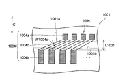
- the wiring 1004 includes an IC pad portion 1004a electrically connected to the electrode 1002a (see FIG. 21) of the driver IC 1002, and an FPC pad portion 1004b electrically connected to the electrode 1003a (see FIG. 21) of the FPC 1003. And a connecting portion 1004c for connecting them.
- the IC pad portion 1004a is disposed in the chip mounting area 1001a
- the FPC pad portion 1004b is disposed in the FPC mounting area 1001b.
- the driver IC 1002 and the FPC 1003 are electrically connected to the IC pad portion 1004a and the FPC pad portion 1004b via an ACF (anisotropic conductive film (anisotropic conductive layer)) not shown.
- the wiring 1004 is not formed of Cu foil but is formed by, for example, a sputtering method or a CVD (Chemical Vapor Deposition) method.
- the wiring 1004 is usually formed as a thin film having a thickness of several tens of nm to several hundreds of nm. For this reason, the wiring 1004 has higher wiring resistance than a circuit board using Cu foil.
- Patent Document 1 a display module including a semiconductor chip and a flexible printed circuit board and a display panel on which the semiconductor chip and the flexible printed circuit board are mounted is disclosed in Patent Document 1, for example.
- the width W1004a of the IC pad portion 1004a is reduced.
- the line width W1004c of the connecting portion 1004c is reduced, and the wiring resistance is increased.
- the width W1004b of the FPC pad portion 1004b is reduced.
- the line width W1004c of the connection part 1004c becomes narrower, and the wiring resistance becomes larger.
- the driver IC 1002 is shrunk, and the FPC 1003 is downsized at the same time, the line width W1004c of the connection portion 1004c is further reduced and the wiring resistance is further increased as shown in FIG. .
- the wiring resistance increases in this way, the wiring resistance does not fall below the load resistance suitable for driving the driver IC 1002, voltage drop and signal delay occur, and quality display cannot be performed.
- the present invention has been made to solve the above-described problems, and an object of the present invention is to provide a display module capable of suppressing an increase in wiring resistance between a semiconductor chip and a mounting component. Is to provide.
- a display module of the present invention includes a display panel including a wiring pattern having a first electrode portion and a second electrode portion, and a first electrode portion disposed on the first electrode portion and electrically connected to the first electrode portion.
- a semiconductor chip including an electrode to be connected, a mounting component including an electrode disposed on the second electrode portion and electrically connected to the second electrode portion, and a wiring pattern are provided separately from the first electrode portion and the first electrode portion.
- a connecting member that electrically connects the two electrode portions to each other.
- connection member that electrically connects the first electrode portion and the second electrode portion to each other is provided separately from the wiring pattern. As a result, for example, even when the line width of the connection portion connecting the first electrode portion and the second electrode portion is narrowed, the resistance between the first electrode portion and the second electrode portion is increased. It can be suppressed by the member.
- the display panel includes a chip mounting area on which a semiconductor chip is mounted and a component mounting area on which a mounting component is mounted, and the wiring pattern extends from the first electrode portion to the outside of the chip mounting area.
- connection member can be connected to the second extension portion outside the component mounting region, and the connection member can be easily electrically connected to the second electrode portion.
- connection member can be easily electrically connected to the second electrode portion.
- connection member preferably includes a paste wiring formed of a conductive paste. If comprised in this way, a 1st electrode part and a 2nd electrode part can be electrically connected mutually easily using the dispenser method, the inkjet method, or the printing method.
- the mounted component may include a flexible printed board.
- the wiring pattern may be formed of the same layer as the first electrode portion and the second electrode portion, and may have a connection portion that connects the first electrode portion and the second electrode portion. In this case, it is not necessary to perform the electrical connection by the connecting member to the electrode portion that does not require a reduction in resistance. Further, if the first electrode portion and the second electrode portion are electrically connected by the connecting member and the connecting portion, it is possible to further suppress an increase in resistance between the first electrode portion and the second electrode portion. . Moreover, even when the connection member or the connection portion is deteriorated, the electrical connection between the first electrode portion and the second electrode portion can be ensured.
- the wiring pattern has a connection portion
- the wiring pattern has a plurality of first electrode portions, a plurality of second electrode portions, and a plurality of connection portions, and at least a part of the connection portion is on the connection portion.
- An insulating film is formed, and the connecting member is disposed up to the adjacent insulating film. If comprised in this way, the line
- the first electrode portion and the second electrode portion may not be electrically connected to each other in the display panel, but may be electrically connected to each other by a connecting member. If comprised in this way, since the 1st electrode part and the 2nd electrode part are not connected beforehand, the 1st electrode part and the 2nd electrode part can be connected with a connecting member according to a specification. Thereby, it is not necessary to manufacture a display panel for every specification, and a display panel can be made common and standardized.
- an insulating protective layer is preferably provided on the connection member. If comprised in this way, it can suppress that a connection member deteriorates or short-circuits adjacent connection members, and can improve the reliability of a display module.
- the electrode of the semiconductor chip preferably includes a bump electrode.
- the semiconductor chip and the mounted component are electrically connected to the display panel via an anisotropic conductive layer.
- connection member that electrically connects the first electrode portion and the second electrode portion to each other is provided separately from the wiring pattern.
- the connection member that electrically connects the first electrode portion and the second electrode portion to each other is provided separately from the wiring pattern.
- FIG. 4 is a sectional view taken along line 100-100 in FIG. It is an enlarged plan view for demonstrating the structure of the wiring of 1st Embodiment of this invention. It is an enlarged plan view for demonstrating the structure of the modification of the wiring of 1st Embodiment of this invention. It is an enlarged plan view for demonstrating the structure of the insulating film of 1st Embodiment of this invention.
- FIG. 14 is a cross-sectional view taken along line 200-200 in FIG. It is an enlarged plan view for demonstrating the structure of the insulating film of 2nd Embodiment of this invention. It is an enlarged plan view for demonstrating the structure of the electrically conductive film of 2nd Embodiment of this invention. It is an enlarged plan view for demonstrating the structure of the wiring pattern of 3rd Embodiment of this invention. It is an enlarged plan view for demonstrating the structure of the paste wiring of 3rd Embodiment of this invention.
- FIG. 19 is a cross-sectional view taken along line 300-300 in FIG.
- FIG. 19 is a cross-sectional view taken along line 350-350 in FIG.
- FIG. 22 is an enlarged plan view showing the structure of the display panel of the display module according to the conventional example shown in FIG. 21.
- FIG. 23 is an enlarged plan view showing a state in which the distance between the IC pad portion and the FPC pad portion of FIG. 22 is shortened.
- FIG. 23 is an enlarged plan view showing a state where the width of the IC pad portion of FIG. 22 is reduced.
- FIG. 25 is an enlarged plan view showing a state in which the width of the FPC pad portion of FIG. 24 is reduced.
- FIG. 23 is an enlarged plan view showing a state in which the distance between the IC pad portion and the FPC pad portion of FIG. 22 is shortened and the width of the IC pad portion and the width of the FPC pad portion are reduced.
- hatching may be performed even in a cross-sectional view, or hatching may be performed even in a cross-sectional view.
- the display module 1 is used for a liquid crystal display device (not shown).
- the display module 1 includes a display panel 10, a semiconductor chip 20 mounted on the display panel 10, and an FPC 30 (mounting component).
- the display panel 10 is configured by combining an AM substrate (active matrix substrate) 11 made of a glass substrate and a counter substrate 12.
- a liquid crystal (not shown) is sealed between the AM substrate 11 and the counter substrate 12.
- the AM substrate 11 has a larger area than the counter substrate 12, and a part of the AM substrate 11 protrudes from the counter substrate 12.
- the semiconductor chip 20 and the FPC 30 are mounted on the protruding portion of the AM substrate 11.
- ACF (anisotropic conductive film (anisotropic conductive layer)) 40 and 41 are disposed between the display panel 10 and the semiconductor chip 20 and between the display panel 10 and the FPC 30, respectively.
- the detailed structure of the display panel 10 will be described later.
- the semiconductor chip 20 is a driver IC for driving liquid crystal.
- the semiconductor chip 20 is formed with wirings and circuit elements (not shown).
- a plurality of input bump electrodes 21 (electrodes, bump electrodes) (see FIG. 2) and a plurality of output bump electrodes (not shown) are electrically connected to the circuit elements. It is connected to the.
- the semiconductor chip 20 is formed in an elongated shape, and the plurality of input bump electrodes 21 are arranged at a predetermined pitch along the longitudinal direction (A direction) of the semiconductor chip 20 as shown in FIG. As shown in FIG. 4, the input bump electrode 21 and the output bump electrode (not shown) are formed so as to protrude from the main surface of the semiconductor chip 20 (the lower surface in FIG. 4).
- the FPC 30 is arranged at a predetermined distance from the semiconductor chip 20 in the B direction (direction orthogonal to the A direction).
- the FPC 30 is formed with a plurality of electrode portions 31 (electrodes), capacitors (not shown) and LEDs, and wiring portions (not shown) connected to the electrode portions 31 and the like.
- the electrodes 31 are arranged at a predetermined pitch in parallel with the input bump electrodes 21 of the semiconductor chip 20 (in the A direction).
- the AM substrate 11 of the display panel 10 includes a chip mounting area 11a on which the semiconductor chip 20 is mounted and an FPC mounting area 11b (component mounting area) on which the FPC 30 is mounted.
- a wiring pattern 13 including a plurality of wirings 130 and conductive films 131 a and 131 b provided on the wirings 130 is formed in a predetermined region on the AM substrate 11.
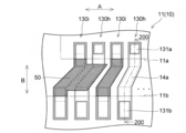
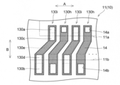
- the wiring 130 is a thin film formed by, for example, a sputtering method or a CVD method, and has a thickness of several tens to several hundreds of nm. As shown in FIG. 5, at both ends of each wiring 130, a pad electrode portion 130 a to which the input bump electrode 21 of the semiconductor chip 20 is electrically connected, and a pad electrode portion to which the electrode portion 31 of the FPC 30 is electrically connected. 130b. Note that hatched areas in FIG. 5 and FIG. 6 to be described later indicate pad electrode portions 130a and 130b.
- the pad electrode portion 130a and the portion of the conductive film 131a (see FIG. 4) on the pad electrode portion 130a constitute the “first electrode portion” of the present invention.
- the “second electrode portion” of the present invention is constituted by the pad electrode portion 130b and the portion of the conductive film 131b (see FIG. 4) on the pad electrode portion 130b.
- the plurality of pad electrode portions 130a are disposed in the chip mounting region 11a and are disposed at positions corresponding to the plurality of input bump electrodes 21 of the semiconductor chip 20, respectively.
- the plurality of pad electrode portions 130b are disposed in the FPC mounting region 11b and are disposed at positions corresponding to the plurality of electrode portions 31 of the FPC 30, respectively.
- the pad electrode part 130b has a larger width in the A direction and is arranged at a larger pitch than the pad electrode part 130a.
- the wiring 130 includes an extending portion 130c extending from the pad electrode portion 130a to the outside of the chip mounting region 11a, and an extending portion 130d extending from the pad electrode portion 130b to the outside of the FPC mounting region 11b. And a connecting portion 130e.
- the pad electrode portions 130a and 130b, the extension portions 130c and 130d, and the connection portion 130e are formed of the same layer.
- the extending portion 130c and the portion on the extending portion 130c of the conductive film 131a constitute the “first extending portion” of the present invention.
- the extending portion 130d and the portion on the extending portion 130d of the conductive film 131b constitute the “second extending portion” of the present invention.
- the extending part 130c may be formed so as to extend in the direction (B direction) perpendicular to the arrangement direction (A direction) of the pad electrode part 130a as shown in FIG. 5, or as shown in FIG. It may be formed to extend in a direction inclined with respect to the direction.
- the extending portion 130d may be formed to extend in the B direction of the pad electrode portion 130b as shown in FIG. 5, or to extend in a direction inclined with respect to the B direction as shown in FIG. It may be formed.
- the connecting portion 130e is connected to the pad electrode portions 130a and 130b via the extending portions 130c and 130d. That is, the connection part 130e connects the pad electrode parts 130a and 130b to each other. Further, the connecting portion 130e is formed to extend in a direction inclined with respect to the A direction.
- an insulating film 14 is provided so as to cover a predetermined region of the wiring 130.
- the hatched area in FIG. 7 shows the insulating film 14. Openings 14 a and 14 b are formed in the insulating film 14.
- the opening 14 a is formed at a position corresponding to the center portion (a portion other than the edge portion) of the pad electrode portion 130 a and the extending portion 130 c of the wiring 130.
- the opening 14b is formed at a position corresponding to the center portion of the pad electrode portion 130b and the extending portion 130d of the wiring 130.
- the insulating film 14 is formed so as to cover the entire surface of the connection portion 130e.
- the insulating film 14 is provided for each wiring 130 in the figure, the insulating film 14 may be enlarged so that the plurality of wirings 130 are covered with one insulating film 14.
- the conductive film 131a is provided in a predetermined region on the wiring 130 so as to be electrically connected to the pad electrode portion 130a through the opening 14a.
- the conductive film 131b is provided in a predetermined region on the wiring 130 so as to be electrically connected to the pad electrode portion 130b through the opening 14b. Note that the hatched regions in FIG. 8 show the conductive films 131a and 131b.
- the conductive films 131a and 131b are formed of ITO (Indium Tin Oxide) or the like, and are formed with a thickness smaller than that of the wiring 130 by using, for example, a sputtering method or a CVD method.
- the conductive film 131a is formed to have a size in which the pad electrode portion 130a and the extension portion 130c of the wiring 130 are combined, and is disposed to the outside of the chip mounting region 11a.
- the conductive film 131b is formed, for example, in a size that combines the pad electrode portion 130b and the extending portion 130d of the wiring 130, and is disposed to the outside of the FPC mounting region 11b.
- the input bump electrode 21 of the semiconductor chip 20 is disposed on the pad electrode portion 130 a (on the conductive film 131 a) via the ACF 40.
- the ACF 40 is formed of a resin film containing conductive particles (not shown). Due to the conductive particles, the conductive film 131a and the input bump electrode 21 are electrically connected to each other.
- the electrode portion 31 of the FPC 30 is disposed on the pad electrode portion 130b (on the conductive film 131b) via the ACF 41. The conductive film 131b and the electrode part 31 are electrically connected to each other by the conductive particles of the ACF41.
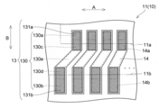
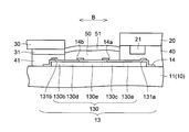
- the paste wiring 50 (on the extended portion 130c (conductive film 131a), the connecting portion 130e (insulating film 14), and the extended portion 130d (conductive film 131b) is provided. Connecting member).
- the hatched area in FIG. 3 shows the paste wiring 50.
- the paste wiring 50 is provided separately from the wiring pattern 13 and is electrically connected to the conductive films 131a and 131b.
- the paste wiring 50 electrically connects the pad electrode portions 130a and 130b to each other.
- the paste wiring 50 is formed of a conductive paste such as Ag paste or Cu paste and has a thickness of several ⁇ m or more. For this reason, it is possible to suppress an increase in wiring resistance between the conductive film 131a and the conductive film 131b.
- the paste wiring 50 is formed after the manufacturing process of the AM substrate 11 (the forming process of the wiring 130 and the insulating film 14).
- the paste wiring 50 can be easily formed using a dispenser method, an inkjet method, a printing method, or the like.
- the paste wiring 50 may be formed with a line width similar to that of the wiring 130, or may be formed with a line width similar to that of the insulating film 14.
- the paste wiring 50 may be formed with a line width larger than that of the insulating film 14 or may be formed with a line width smaller than that of the wiring 130.
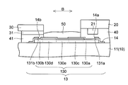
- a protective layer 51 covering the paste wiring 50 may be provided on the paste wiring 50.
- This protective layer 51 may be formed of, for example, an insulating resin.
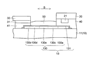
- the openings 14a and 14b of the insulating film 14 are formed up to the extending portions 130c and 130d, but the present invention is not limited to this.
- the opening 14a may not be formed up to the extending portion 130c.
- the opening 14b may not be formed up to the extending portion 130d.
- the conductive films 131a and 131b are formed to the outside of the chip mounting region 11a and the FPC mounting region 11b, the pad electrode part 130a and the pad electrode part 130b can be easily connected to each other by the paste wiring 50. Electrical connection is possible.
- the insulating film 14 is provided on the wiring 130 .
- the insulating film 14 may not be provided.
- the conductive film 131 may be provided so as to cover the entire surface of the wiring 130.
- the present invention is not limited to this.
- the width of the paste wiring 50 disposed on the wiring 130f is reduced, and the paste wiring 50 disposed on the wiring 130g is disposed up to the adjacent wiring 130f (insulating film 14).
- the hatched area in FIG. 12 shows the paste wiring 50.
- the mounting process of the semiconductor chip 20, the mounting process of the FPC 30, and the forming process of the paste wiring 50 may be performed in any order.
- the paste wiring 50 may be formed by applying and curing a conductive paste.
- the conductive paste, ACFs 40 and 41 may be cured after applying the conductive paste and mounting the semiconductor chip 20 and the FPC 30 using the ACFs 40 and 41.
- the paste wiring 50 that electrically connects the pad electrode portion 130a and the pad electrode portion 130b to each other is provided separately from the wiring pattern 13. Thereby, even if the line width of the connection part 130e becomes thin, it can suppress by the paste wiring 50 that resistance between the pad electrode part 130a and the pad electrode part 130b becomes large. That is, even when the display panel 10 is narrowed or the semiconductor chip 20 is shrunk, an increase in resistance between the pad electrode portion 130a and the pad electrode portion 130b can be suppressed. For this reason, it is possible to suppress a voltage drop or a signal delay, and to suppress a deterioration in display quality.
- the wiring 130 extends from the pad electrode portion 130a to the outside of the chip mounting region 11a, and extends from the pad electrode portion 130b to the outside of the FPC mounting region 11b.
- the paste wiring 50 is connected to the extending part 130c and the extending part 130d. Thereby, the paste wiring 50 can be connected to the extending portion 130c outside the chip mounting region 11a, and the paste wiring 50 can be easily electrically connected to the pad electrode portion 130a.
- the paste wiring 50 can be connected to the extending portion 130d outside the FPC mounting region 11b, and the paste wiring 50 can be easily electrically connected to the pad electrode portion 130b. Thereby, the pad electrode part 130a and the pad electrode part 130b can be easily electrically connected to each other using the paste wiring 50.
- the pad electrode portion 130a and the pad electrode portion 130b can be easily electrically connected to each other using a dispenser method, an inkjet method, a printing method, or the like. Can be connected to.
- the resistance between the pad electrode portion 130a and the pad electrode portion 130b is increased by electrically connecting the pad electrode portion 130a and the pad electrode portion 130b with the connection portion 130e and the paste wiring 50. Can be further suppressed. Further, even when the connection portion 130e or the paste wiring 50 is deteriorated, the electrical connection between the pad electrode portion 130a and the pad electrode portion 130b can be ensured.
- the line width of the paste wiring 50 on the wiring 130g is further increased. be able to. Thereby, it is possible to further suppress an increase in resistance between the pad electrode portions 130a and 130b of the wiring 130g.
- the insulating protective layer 51 is provided on the paste wiring 50, it can suppress that the paste wiring 50 deteriorates or adjacent paste wiring 50 is short-circuited. . Thereby, the reliability of the display module 1 can be improved.
- the display panel 10 according to the second embodiment of the present invention includes a wiring 130h that does not require a low resistance and a wiring 130i that requires a low resistance as in the first embodiment (for example, a power supply wiring). ).
- the openings 14 a and 14 b of the insulating film 14 formed on the wiring 130 h that does not require resistance reduction are the insulating films 14 formed on the wiring 130 i that require resistance reduction. Smaller than the openings 14a and 14b. Specifically, the opening 14a of the insulating film 14 on the wiring 130h is not formed up to the extending part 130c, and the opening 14b is not formed up to the extending part 130d. Note that the openings 14a and 14b of the insulating film 14 on the wiring 130i that need to have a low resistance need not be formed up to the extending portions 130c and 130d.
- the hatched area in FIG. 15 shows the insulating film 14.
- the conductive films 131 a and 131 b formed over the wiring 130 h that does not require a lower resistance than the conductive films 131 a and 131 b formed over the wiring 130 i that needs a lower resistance. small. Specifically, the conductive film 131a on the wiring 130h is not formed to the outside of the chip mounting region 11a, and the conductive film 131b is not formed to the outside of the FPC mounting region 11b. Note that the hatched regions in FIG. 16 indicate the conductive films 131a and 131b.
- the paste wiring 50 is not provided on the wiring 130h that does not require resistance reduction, and the pad electrode portion 130a and the pad electrode portion 130b are extended portions 130c, connecting portions 130e, and The extension part 130d is electrically connected.
- a paste wiring 50 is provided on the wiring 130i that needs to have a low resistance.
- the paste wiring 50 may be disposed up to the adjacent insulating film 14. Note that the hatched area in FIG. 13 shows the paste wiring 50.
- the paste wiring 50 disposed on the wiring 130i is disposed up to the adjacent wiring 130h (insulating film 14), thereby increasing the line width of the paste wiring 50 on the wiring 130i. can do.
- the line width of the paste wiring 50 on the wiring 130i can be made larger than that of the paste wiring 50 on the wiring 130g shown in FIG. 12, and the resistance between the pad electrode portions 130a and 130b is increased. Further suppression can be achieved.
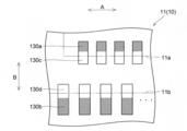
- the wiring pattern 13 is not provided with the connecting portion 130e.
- the pad electrode part 130a and the pad electrode part 130b are not electrically connected to each other.
- the insulating film 14 is not particularly required, the insulating film 14 is not provided.
- the hatched area in FIG. 17 shows the pad electrode portions 130a and 130b.
- the pad electrode portions 130a and 130b that require electrical connection are electrically connected to each other by the paste wiring 50.
- pad electrode portions 130a and 130b that do not require electrical connection are not electrically connected to each other.
- the hatched area in FIG. 18 shows the paste wiring 50.
- the pad electrode portion 130a and the pad electrode portion 130b are not electrically connected to each other in the display panel 10, and only the electrode portions that need to be connected are connected by the paste wiring 50.
- the pad electrode part 130a and the pad electrode part 130b are not connected in advance, and the pad electrode part 130a and the pad electrode part 130b are connected by the paste wiring 50 in accordance with specifications.
- the semiconductor chip 20 can be shared and standardized to some extent, and one type of semiconductor chip 20 can be applied to a plurality of customer specifications.
- the pad electrode portions 130a and 130b for inputting signals are selected so as to meet customer specifications, and only the pad electrode portions to be used are wired. For this reason, the number of types of display panels 10 is required by the number of customer specifications, and the number of types of display panels 10 increases. In the present embodiment, since the display panel 10 can be made common and standardized, an increase in the types of the display panel 10 can be suppressed, which is particularly effective.
- the present invention is not limited to this and may be applied to a display module other than the liquid crystal display module.
- the FPC is taken as an example of a mounting component mounted on the display panel, but the present invention is not limited to this.
- a mounting component such as a capacitor or LED may be mounted on the display panel, and the capacitor or LED and the semiconductor chip may be electrically connected to each other by paste wiring (connection member).
- connection member an example in which the paste wiring is used as the connection member has been described, but the present invention is not limited to this.
- a metal wire may be used as the connection member, and the conductive films 131a and 131b may be electrically connected by wire bonding.
- the present invention is not limited thereto, and the conductive film may not be provided on the pad electrode portion.
- ACF anisotropic conductive paste (anisotropic conductive layer)
- anisotropic conductive layer anisotropic conductive layer
- the present invention is not limited thereto, and the bump electrode may not be provided on the semiconductor chip.
- the present invention is not limited to this.
- the pad electrode portions 130a and 130b are not electrically connected to each other in the display panel 10, the extending portions 130c and 130d need not be provided.
- the pitch of the second electrode part (pad electrode part 130b) is larger than the pitch of the first electrode part (pad electrode part 130a) has been described, but the present invention is not limited to this.
- the pitch of the second electrode part may be the same as or smaller than the pitch of the first electrode part. That is, the pitch of the electrodes of the mounting component (FPC or the like) may be the same as or smaller than the pitch of the electrodes of the semiconductor chip.
Landscapes
- Physics & Mathematics (AREA)
- Nonlinear Science (AREA)
- Mathematical Physics (AREA)
- Chemical & Material Sciences (AREA)
- Crystallography & Structural Chemistry (AREA)
- General Physics & Mathematics (AREA)
- Optics & Photonics (AREA)
- Liquid Crystal (AREA)
Abstract
半導体チップと実装部品との間の配線抵抗が大きくなるのを抑制することが可能な表示モジュールを提供する。この表示モジュール(1)は、パッド電極部(130a)およびパッド電極部(130b)を有する配線パターン(13)を含む表示パネル(10)と、パッド電極部(130a)に電気的に接続される半導体チップ(20)と、パッド電極部(130b)に電気的に接続されるFPC(30)と、配線パターンとは別に設けられ、パッド電極部(130a)およびパッド電極部(130b)を互いに電気的に接続するペースト配線(50)と、を備える。
Description
この発明は、表示モジュールに関し、特に、半導体チップおよび実装部品が実装される表示パネルを備えた表示モジュールに関する。
近年、テレビジョン受像機やコンピュータのモニタなど様々な機器に表示装置が用いられている。また、様々な表示装置に表示モジュールが用いられており、半導体チップおよび実装部品とそれらが実装される表示パネルとを備えた表示モジュールが知られている。図21は従来の一例による表示モジュールの構造の一部を示した平面図である。図22は図21に示した従来の一例による表示モジュールの表示パネルの構造を示した拡大平面図である。従来の一例による表示モジュールは図21に示すように、表示パネル1001と、表示パネル1001を駆動するドライバIC(半導体チップ)1002と、表示パネル1001に外部信号を入力するFPC(フレキシブルプリント基板)1003とを備えている。表示パネル1001は図22に示すように、ドライバIC1002が実装されるチップ実装領域1001aと、FPC1003が実装されるFPC実装領域1001bとを含んでいる。
また、表示パネル1001には、複数の配線1004が形成されている。この配線1004はドライバIC1002の電極1002a(図21参照)に電気的に接続されるIC用パッド部1004aと、FPC1003の電極1003a(図21参照)に電気的に接続されるFPC用パッド部1004bと、それらを接続する接続部1004cとを含んでいる。IC用パッド部1004aはチップ実装領域1001a内に配置されており、FPC用パッド部1004bはFPC実装領域1001b内に配置されている。ドライバIC1002およびFPC1003は、図示しないACF(異方性導電フィルム(異方性導電層))を介してIC用パッド部1004aおよびFPCパッド部1004bにそれぞれ電気的に接続されている。
表示パネル1001はガラス基板により形成されているため、配線1004はCu箔でなく例えばスパッタ法やCVD(Chemical Vapor Deposition)法により形成される。配線1004は、通常、数十nm~数百nmの厚みを有する薄膜に形成される。このため、配線1004はCu箔を用いた回路基板などに比べて配線抵抗が大きくなる。
なお、半導体チップおよびフレキシブルプリント基板とそれらが実装された表示パネルとを備えた表示モジュールは、例えば特許文献1に開示されている。
ところで近年、表示パネルの狭額縁化やドライバIC(半導体チップ)のシュリンク化などが望まれている。表示パネル1001を狭額縁化する場合、図23に示すように、IC用パッド部1004aの配列方向に対して垂直な方向(C方向)における、IC用パッド部1004aとFPC用パッド部1004bとの間の距離L1001が短くなる。このため、接続部1004cの線幅W1004cが細くなり、配線抵抗が大きくなる。
一方、ドライバIC1002をシュリンク化する場合、図24に示すように、IC用パッド部1004aの幅W1004aが小さくなる。このため、接続部1004cの線幅W1004cが細くなり、配線抵抗が大きくなる。さらに、FPC1003を小型化する場合、図25に示すように、FPC用パッド部1004bの幅W1004bが小さくなる。このため、接続部1004cの線幅W1004cがより細くなり、配線抵抗がより大きくなる。
そして、表示パネル1001の狭額縁化、ドライバIC1002のシュリンク化およびFPC1003の小型化を同時に行うと、図26に示すように、接続部1004cの線幅W1004cはさらに細くなり、配線抵抗がさらに大きくなる。
このように配線抵抗が大きくなると、ドライバIC1002を駆動するのに適した負荷抵抗以下に配線抵抗がならず電圧降下や信号遅延が起こり、品位ある表示ができなくなる。
この発明は、上記のような課題を解決するためになされたものであり、この発明の目的は、半導体チップと実装部品との間の配線抵抗が大きくなるのを抑制することが可能な表示モジュールを提供することである。
上記目的を達成するために、この発明の表示モジュールは、第1電極部および第2電極部を有する配線パターンを含む表示パネルと、第1電極部上に配置され第1電極部に電気的に接続される電極を含む半導体チップと、第2電極部上に配置され第2電極部に電気的に接続される電極を含む実装部品と、配線パターンとは別に設けられ、第1電極部および第2電極部を互いに電気的に接続する接続部材と、を備える。
この表示モジュールでは、上記のように、第1電極部および第2電極部を互いに電気的に接続する接続部材を、配線パターンとは別に設ける。これにより、例えば第1電極部および第2電極部を接続する接続部の線幅が細くなった場合であっても、第1電極部および第2電極部の間の抵抗が大きくなるのを接続部材により抑制することができる。
上記表示モジュールにおいて、好ましくは、表示パネルは半導体チップが実装されるチップ実装領域と、実装部品が実装される部品実装領域とを含み、配線パターンは第1電極部からチップ実装領域の外側まで延在された第1延在部と、第2電極部から部品実装領域の外側まで延在された第2延在部とを有し、接続部材は第1延在部と第2延在部とに接続されている。このように構成すれば、チップ実装領域の外側で接続部材を第1延在部に接続し、接続部材を容易に第1電極部に電気的に接続させることができる。同様に、部品実装領域の外側で接続部材を第2延在部に接続し、接続部材を容易に第2電極部に電気的に接続させることができる。これにより、接続部材を用いて容易に、第1電極部および第2電極部を互いに電気的に接続することができる。
上記表示モジュールにおいて、好ましくは、接続部材は導電性ペーストにより形成されたペースト配線を含む。このように構成すれば、ディスペンサ法、インクジェット法または印刷法などを用いて容易に、第1電極部および第2電極部を互いに電気的に接続することができる。
上記表示モジュールにおいて、実装部品はフレキシブルプリント基板を含んでいてもよい。
上記表示モジュールにおいて、配線パターンは第1電極部および第2電極部と同一の層からなるとともに第1電極部および第2電極部を接続する接続部を有してもよい。この場合、低抵抗化が必要でない電極部に対しては、接続部材による電気的接続を行わなくてもよい。また、第1電極部および第2電極部を接続部材と接続部とにより電気的に接続すれば、第1電極部および第2電極部の間の抵抗が大きくなるのをより抑制することができる。また、接続部材または接続部が劣化した場合であっても、第1電極部および第2電極部の間の電気的接続を確保することができる。
上記配線パターンが接続部を有する表示モジュールにおいて、好ましくは、配線パターンは、複数の第1電極部、複数の第2電極部および複数の接続部を有し、接続部上の少なくとも一部には絶縁膜が形成されており、接続部材は隣接する絶縁膜上まで配置されている。このように構成すれば、接続部材の線幅をより大きくすることができる。
上記表示モジュールにおいて、第1電極部および第2電極部は、表示パネル内において互いに電気的に接続されておらず、接続部材により互いに電気的に接続されてもよい。このように構成すれば、第1電極部と第2電極部とが予め接続されていないので、仕様に合わせて第1電極部および第2電極部を接続部材により接続することができる。これにより、仕様毎に表示パネルを製造する必要がなく、表示パネルを共通化・標準化することができる。
上記表示モジュールにおいて、好ましくは、接続部材上には絶縁性の保護層が設けられている。このように構成すれば、接続部材が劣化したり、隣接する接続部材同士が短絡するのを抑制することができ、表示モジュールの信頼性を向上させることができる。
上記表示モジュールにおいて、好ましくは、半導体チップの電極はバンプ電極を含む。
上記表示モジュールにおいて、好ましくは、半導体チップおよび実装部品は表示パネルに異方性導電層を介して電気的に接続される。
以上のように、本発明によれば、第1電極部および第2電極部を互いに電気的に接続する接続部材を、配線パターンとは別に設ける。これにより、例えば第1電極部および第2電極部を接続する接続部の線幅が細くなった場合であっても、第1電極部および第2電極部の間の抵抗が大きくなるのを接続部材により抑制することができる。すなわち、表示パネルの狭額縁化や半導体チップのシュリンク化などを行った場合であっても、第1電極部および第2電極部の間の抵抗が大きくなるのを抑制することができる。このため、電圧降下や信号遅延が起こるのを抑制することができ、表示品位が低下するのを抑制することができる。
以下、本発明の実施形態について図面を参照して説明する。なお、理解を容易にするために、断面図であってもハッチングを施さない場合や、断面図でなくてもハッチングを施す場合がある。
(第1実施形態)
図1~図12を参照して、本発明の第1実施形態による表示モジュール1の構造について説明する。
図1~図12を参照して、本発明の第1実施形態による表示モジュール1の構造について説明する。
本発明の第1実施形態による表示モジュール1は液晶表示装置(図示せず)に用いられるものである。また、表示モジュール1は図1に示すように、表示パネル10と、表示パネル10に実装される半導体チップ20およびFPC30(実装部品)とを備えている。表示パネル10は、いずれもガラス基板からなるAM基板(アクティブマトリックス基板)11と対向基板12とを合わせて構成されている。また、AM基板11と対向基板12との間には、図示しない液晶が封入されている。AM基板11は対向基板12よりも面積が大きく、一部が対向基板12からはみ出している。AM基板11のはみ出し部分に半導体チップ20およびFPC30が実装されている。表示パネル10および半導体チップ20の間と、表示パネル10およびFPC30の間とには、ACF(異方性導電フィルム(異方性導電層))40および41がそれぞれ配置されている。表示パネル10の詳細な構造は後述する。
半導体チップ20は液晶駆動用のドライバICである。半導体チップ20には図示しない配線や回路素子などが形成されており、この回路素子に複数の入力バンプ電極21(電極、バンプ電極)(図2参照)および図示しない複数の出力バンプ電極が電気的に接続されている。また、半導体チップ20は細長形状に形成されており、複数の入力バンプ電極21は図2に示すように半導体チップ20の長手方向(A方向)に沿って所定のピッチで配列されている。なお、入力バンプ電極21および図示しない出力バンプ電極は図4に示すように、半導体チップ20の主表面(図4の下面)から突出するように形成されている。
FPC30は図2に示すように、半導体チップ20からB方向(A方向と直交する方向)に所定の距離を隔てて配置されている。FPC30には複数の電極部31(電極)と、図示しないコンデンサおよびLEDと、電極部31などに接続される図示しない配線部とが形成されている。また、電極31は半導体チップ20の入力バンプ電極21と平行に(A方向に)所定のピッチで配列されている。
次に、表示パネル10の詳細な構造を説明する。
表示パネル10のAM基板11は図5に示すように、半導体チップ20が実装されるチップ実装領域11aと、FPC30が実装されるFPC実装領域11b(部品実装領域)とを含んでいる。AM基板11上の所定領域には図4に示すように、複数の配線130と配線130上に設けられた導電膜131aおよび131bとを含む配線パターン13が形成されている。
配線130は例えばスパッタ法やCVD法により形成された薄膜であり、数十nm~数百nmの厚みに形成されている。各配線130の両端には図5に示すように、半導体チップ20の入力バンプ電極21が電気的に接続されるパッド電極部130aと、FPC30の電極部31が電気的に接続されるパッド電極部130bとが設けられている。なお、図5および後述する図6のハッチング領域は、パッド電極部130aおよび130bを示している。パッド電極部130aと導電膜131a(図4参照)のパッド電極部130a上の部分とによって、本発明の「第1電極部」が構成されている。また、パッド電極部130bと導電膜131b(図4参照)のパッド電極部130b上の部分とによって、本発明の「第2電極部」が構成されている。
複数のパッド電極部130aはチップ実装領域11a内に配置されているとともに、半導体チップ20の複数の入力バンプ電極21にそれぞれ対応する位置に配置されている。複数のパッド電極部130bはFPC実装領域11b内に配置されているとともに、FPC30の複数の電極部31にそれぞれ対応する位置に配置されている。パッド電極部130bはパッド電極部130aに比べて、A方向に大きい幅を有するとともに大きいピッチで配列されている。
また、配線130には、パッド電極部130aからチップ実装領域11aの外側まで延在された延在部130cと、パッド電極部130bからFPC実装領域11bの外側まで延在された延在部130dと、接続部130eとが設けられている。パッド電極部130a、130b、延在部130c、130dおよび接続部130eは同一の層で形成されている。なお、延在部130cと導電膜131a(図4参照)の延在部130c上の部分とによって、本発明の「第1延在部」が構成されている。また、延在部130dと導電膜131b(図4参照)の延在部130d上の部分とによって、本発明の「第2延在部」が構成されている。
延在部130cは図5に示すようにパッド電極部130aの配列方向(A方向)に対して垂直方向(B方向)に延びるように形成されていてもよいし、図6に示すようにB方向に対して傾斜する方向に延びるように形成されていてもよい。同様に、延在部130dは図5に示すようにパッド電極部130bのB方向に延びるように形成されていてもよいし、図6に示すようにB方向に対して傾斜する方向に延びるように形成されていてもよい。
接続部130eは延在部130cおよび130dを介してパッド電極部130aおよび130bに接続されている。すなわち、接続部130eはパッド電極部130aおよび130bを互いに接続している。また、接続部130eはA方向に対して傾斜する方向に延びるように形成されている。
図4および図7に示すように、配線130の所定の領域を覆うように絶縁膜14が設けられている。なお、図7のハッチング領域は、絶縁膜14を示している。この絶縁膜14には開口部14aおよび14bが形成されている。開口部14aは図7に示すように、配線130のパッド電極部130aと延在部130cとの中央部(縁部以外の部分)に対応する位置に形成されている。開口部14bは、配線130のパッド電極部130bと延在部130dとの中央部に対応する位置に形成されている。また、絶縁膜14は接続部130eの全面を覆うように形成されている。なお、図では絶縁膜14は配線130毎に設けられているが、絶縁膜14を大きくして1つの絶縁膜14で複数の配線130を覆うようにしてもよい。
導電膜131aは図4および図8に示すように、開口部14aを介してパッド電極部130aと電気的に接続するように、配線130上の所定領域に設けられている。導電膜131bは開口部14bを介してパッド電極部130bと電気的に接続するように、配線130上の所定領域に設けられている。なお、図8のハッチング領域は、導電膜131aおよび131bを示している。導電膜131aおよび131bはITO(Indium Tin Oxide)などにより形成されているとともに、例えばスパッタ法やCVD法を用いて配線130よりも小さい厚みに形成されている。導電膜131aは例えば配線130のパッド電極部130aと延在部130cとを合わせた大きさに形成されており、チップ実装領域11aの外側まで配置されている。同様に、導電膜131bは例えば配線130のパッド電極部130bと延在部130dとを合わせた大きさに形成されており、FPC実装領域11bの外側まで配置されている。
パッド電極部130a上(導電膜131a上)には図4に示すように、ACF40を介して半導体チップ20の入力バンプ電極21が配置されている。ACF40は図示しない導電粒子を含有する樹脂フィルムにより形成されている。この導電粒子により、導電膜131aと入力バンプ電極21とが互いに電気的に接続されている。同様に、パッド電極部130b上(導電膜131b上)には、ACF41を介してFPC30の電極部31が配置されている。ACF41の導電粒子により、導電膜131bと電極部31とが互いに電気的に接続されている。
ここで、図3および図4に示すように、延在部130c(導電膜131a)、接続部130e(絶縁膜14)および延在部130d(導電膜131b)の上には、ペースト配線50(接続部材)が設けられている。なお、図3のハッチング領域は、ペースト配線50を示している。このペースト配線50は配線パターン13とは別に設けられているとともに、導電膜131aおよび131bに電気的に接続されている。ペースト配線50は、パッド電極部130aおよび130bを互いに電気的に接続している。また、ペースト配線50はAgペーストやCuペーストなどの導電性ペーストにより形成されており、数μm以上の厚みを有する。このため、導電膜131aと導電膜131bとの間の配線抵抗が大きくなるのを抑制することが可能である。ペースト配線50はAM基板11の製造工程(配線130や絶縁膜14などの形成工程)の後で形成されるものである。ペースト配線50はディスペンサ法、インクジェット法または印刷法などを用いて容易に形成することが可能である。
ペースト配線50は図3に示すように、配線130と同程度の線幅に形成されていてもよいし、絶縁膜14と同程度の線幅に形成されていてもよい。また、ペースト配線50は絶縁膜14よりも大きい線幅に形成されていてもよいし、配線130よりも小さい線幅に形成されていてもよい。
図9に示すように、ペースト配線50上に、ペースト配線50を覆う保護層51が設けられていてもよい。この保護層51は例えば絶縁性の樹脂により形成されていてもよい。
上記の説明では絶縁膜14の開口部14aおよび14bが延在部130cおよび130dまで形成される場合について説明したが、これに限定されるものではない。例えば図10に示すように、開口部14aを延在部130cまで形成しなくてもよい。同様に、開口部14bを延在部130dまで形成しなくてもよい。この場合であっても、導電膜131aおよび131bがチップ実装領域11aおよびFPC実装領域11bの外側までそれぞれ形成されていれば、パッド電極部130aとパッド電極部130bとを容易にペースト配線50により互いに電気的に接続することが可能である。
また、上記の説明では配線130上に絶縁膜14を設ける場合について説明したが、例えば図11に示すように、絶縁膜14を設けなくてもよい。この場合、配線130の全面を覆うように導電膜131を設けてもよい。
また、上記の説明ではペースト配線50が隣接する配線130(絶縁膜14)上まで配置されない場合について説明したが、これに限定されるものではない。例えば図12に示すように、配線130f上に配置されるペースト配線50の幅を小さくし、配線130g上に配置されるペースト配線50を隣接する配線130f(絶縁膜14)上まで配置してもよい。なお、図12のハッチング領域は、ペースト配線50を示している。
表示モジュール1を製造する際には、半導体チップ20の実装工程、FPC30の実装工程およびペースト配線50の形成工程をどのような順序で行ってもよい。例えば、ACF40を用いて半導体チップ20を実装し、ACF41を用いてFPC30を実装した後で、導電性ペーストを塗布・硬化してペースト配線50を形成してもよい。また例えば、導電性ペーストを塗布し、ACF40および41を用いて半導体チップ20およびFPC30を実装した後で、導電性ペースト、ACF40および41を硬化してもよい。
本実施形態では、上記のように、パッド電極部130aおよびパッド電極部130bを互いに電気的に接続するペースト配線50を、配線パターン13とは別に設ける。これにより、接続部130eの線幅が細くなった場合であっても、パッド電極部130aおよびパッド電極部130bの間の抵抗が大きくなるのをペースト配線50により抑制することができる。すなわち、表示パネル10の狭額縁化や半導体チップ20のシュリンク化などを行った場合であっても、パッド電極部130aおよびパッド電極部130bの間の抵抗が大きくなるのを抑制することができる。このため、電圧降下や信号遅延が起こるのを抑制することができ、表示品位が低下するのを抑制することができる。
また、上記のように、配線130はパッド電極部130aからチップ実装領域11aの外側まで延在された延在部130cと、パッド電極部130bからFPC実装領域11bの外側まで延在された延在部130dとを有し、ペースト配線50は延在部130cと延在部130dとに接続されている。これにより、チップ実装領域11aの外側でペースト配線50を延在部130cに接続し、ペースト配線50を容易にパッド電極部130aに電気的に接続させることができる。同様に、FPC実装領域11bの外側でペースト配線50を延在部130dに接続し、ペースト配線50を容易にパッド電極部130bに電気的に接続させることができる。これにより、ペースト配線50を用いて容易に、パッド電極部130aおよびパッド電極部130bを互いに電気的に接続することができる。
また、上記のように、導電性ペーストにより形成されたペースト配線50を用いることによって、ディスペンサ法、インクジェット法または印刷法などを用いて容易に、パッド電極部130aおよびパッド電極部130bを互いに電気的に接続することができる。
また、上記のように、パッド電極部130aおよびパッド電極部130bを接続部130eとペースト配線50とにより電気的に接続することによって、パッド電極部130aおよびパッド電極部130bの間の抵抗が大きくなるのをより抑制することができる。また、接続部130eまたはペースト配線50が劣化した場合であっても、パッド電極部130aおよびパッド電極部130bの間の電気的接続を確保することができる。
また、図12に示したように、配線130g上に配置されるペースト配線50を隣接する配線130f(絶縁膜14)上まで配置すれば、配線130g上のペースト配線50の線幅をより大きくすることができる。これにより、配線130gのパッド電極部130aおよび130bの間の抵抗が大きくなるのをより抑制することができる。
また、図9に示したように、ペースト配線50上に絶縁性の保護層51を設ければ、ペースト配線50が劣化したり、隣接するペースト配線50同士が短絡するのを抑制することができる。これにより、表示モジュール1の信頼性を向上させることができる。
(第2実施形態)
この第2実施形態では図13~図16を参照して、上記第1実施形態と異なり、複数の配線130のうちの一部の配線130iにペースト配線50を設ける場合について説明する。
この第2実施形態では図13~図16を参照して、上記第1実施形態と異なり、複数の配線130のうちの一部の配線130iにペースト配線50を設ける場合について説明する。
本発明の第2実施形態の表示パネル10は図13に示すように、低抵抗化が必要でない配線130hと、上記第1実施形態と同様に低抵抗化が必要な配線130i(例えば電源用配線)とを含んでいる。
図14および図15に示すように、低抵抗化が必要でない配線130h上に形成される絶縁膜14の開口部14aおよび14bは、低抵抗化が必要な配線130i上に形成される絶縁膜14の開口部14aおよび14bよりも小さい。具体的には、配線130h上の絶縁膜14の開口部14aは延在部130cまで形成されておらず、開口部14bは延在部130dまで形成されていない。なお、低抵抗化が必要な配線130i上の絶縁膜14の開口部14aおよび14bも、延在部130cおよび130dまで形成しなくてもよい。図15のハッチング領域は、絶縁膜14を示している。
図14および図16に示すように、低抵抗化が必要でない配線130h上に形成される導電膜131aおよび131bは、低抵抗化が必要な配線130i上に形成される導電膜131aおよび131bよりも小さい。具体的には、配線130h上の導電膜131aはチップ実装領域11aの外側まで形成されておらず、導電膜131bはFPC実装領域11bの外側まで形成されていない。なお、図16のハッチング領域は、導電膜131aおよび131bを示している。
そして、図14に示すように、低抵抗化が必要でない配線130h上にはペースト配線50が設けられておらず、パッド電極部130aとパッド電極部130bとは延在部130c、接続部130eおよび延在部130dにより電気的に接続されている。
その一方、低抵抗化が必要な配線130i上には図13に示すように、ペースト配線50が設けられている。このペースト配線50は隣接する絶縁膜14上まで配置されていてもよい。なお、図13のハッチング領域は、ペースト配線50を示している。
第2実施形態のその他の構造は、上記第1実施形態と同様である。
本実施形態では、上記のように、配線130i上に配置されるペースト配線50を隣接する配線130h(絶縁膜14)上まで配置することによって、配線130i上のペースト配線50の線幅をより大きくすることができる。この場合、配線130i上のペースト配線50の線幅を図12に示した配線130g上のペースト配線50よりもさらに大きくすることができ、パッド電極部130aおよび130bの間の抵抗が大きくなるのをさらに抑制することができる。
なお、第2実施形態のその他の効果は、上記第1実施形態と同様である。
(第3実施形態)
この第3実施形態では図17~図20を参照して、上記第1および第2実施形態と異なり、配線パターン13に接続部130eが設けられていない場合について説明する。なお、説明を簡単にするために、図17および図18では導電膜131aおよび131bを省略して描いている。
この第3実施形態では図17~図20を参照して、上記第1および第2実施形態と異なり、配線パターン13に接続部130eが設けられていない場合について説明する。なお、説明を簡単にするために、図17および図18では導電膜131aおよび131bを省略して描いている。
本発明の第3実施形態では図17に示すように、配線パターン13には接続部130eが設けられていない。このため、表示パネル10内においてパッド電極部130aとパッド電極部130bとは互いに電気的に接続されていない。本実施形態では絶縁膜14を特に必要としないので、絶縁膜14は設けられていない。なお、図17のハッチング領域は、パッド電極部130aおよび130bを示している。
そして、図18および図19に示すように、電気的接続が必要なパッド電極部130aおよび130bはペースト配線50により互いに電気的に接続されている。その一方、図18および図20に示すように、電気的接続が必要でないパッド電極部130aおよび130bは互いに電気的に接続されていない。なお、図18のハッチング領域は、ペースト配線50を示している。
第3実施形態のその他の構造は、上記第1および第2実施形態と同様である。
本実施形態では、上記のように、パッド電極部130aおよびパッド電極部130bは、表示パネル10内において互いに電気的に接続されておらず、接続の必要な電極部だけがペースト配線50により接続される。すなわち、パッド電極部130aとパッド電極部130bとは予め接続されておらず、仕様に合わせてパッド電極部130aおよびパッド電極部130bがペースト配線50により接続される。これにより、仕様毎に表示パネル10を製造する必要がなく、表示パネル10を共通化・標準化することができる。なお、一般的には、半導体チップ20はある程度共通化・標準化が可能であり、1種類の半導体チップ20で複数の顧客仕様に適用可能である。ところが、半導体チップ20のバンプ電極(入力バンプ電極21)は全てが必要というわけではなく、顧客仕様によって必要なバンプ電極と必要でないバンプ電極とが存在する。このため、表示パネル10では、顧客仕様に合うように信号入力するパッド電極部130aおよび130bが選択され、使用するパッド電極部のみが配線される。このため、顧客仕様の数だけ表示パネル10の種類が必要であり、表示パネル10の種類が増える。本実施形態では表示パネル10を共通化・標準化することができるので、表示パネル10の種類が増えるのを抑制することができ、特に有効である。
第3実施形態のその他の効果は、上記第1および第2実施形態と同様である。
なお、今回開示された実施形態は、すべての点で例示であって制限的なものではないと考えられるべきである。本発明の範囲は、上記した実施形態の説明ではなく請求の範囲によって示され、さらに請求の範囲と均等の意味および範囲内でのすべての変更が含まれる。
たとえば、上記実施形態では、表示モジュールを液晶表示モジュールに適用した例について示したが、本発明はこれに限らず、液晶表示モジュール以外の表示モジュールに適用してもよい。
また、上記実施形態では、表示パネルに実装される実装部品の一例としてFPCを例に挙げたが、本発明はこれに限らない。表示パネルに例えばコンデンサやLEDなどの実装部品を実装し、コンデンサやLEDなどと半導体チップとをペースト配線(接続部材)により互いに電気的に接続してもよい。
また、上記実施形態では、接続部材としてペースト配線を用いた例について示したが、本発明はこれに限らない。接続部材として例えば金属線を用いて、ワイヤーボンディングにより導電膜131aおよび131bを電気的に接続してもよい。
また、上記実施形態では、パッド電極部上に導電膜を設けた例について示したが、本発明はこれに限らず、パッド電極部上に導電膜を設けなくてもよい。
また、上記実施形態では、半導体チップおよびFPCを表示パネルに実装する場合にACFを用いた例について示したが、本発明はこれに限らない。半導体チップおよびFPCを表示パネルに実装する場合にACP(異方性導電ペースト(異方性導電層))を用いてもよいし、異方性導電層を介さず直接接続してもよい。
また、上記実施形態では、半導体チップにバンプ電極を設けた例について示したが、本発明はこれに限らず、半導体チップにバンプ電極を設けなくてもよい。
また、上記第3実施形態では、延在部130cおよび130dを設ける例について示したが、本発明はこれに限らない。表示パネル10内においてパッド電極部130aおよび130bを互いに電気的に接続しない場合は、延在部130cおよび130dを設けなくてもよい。この場合、ペースト配線50による電気的接続を容易にするために、導電膜131aをチップ実装領域11aの外側まで形成し、導電膜131bをFPC実装領域11bの外側まで形成することが好ましい。
また、上記実施形態では、第2電極部(パッド電極部130b)のピッチが、第1電極部(パッド電極部130a)のピッチよりも大きい例について示したが、本発明はこれに限らない。第2電極部のピッチが、第1電極部のピッチと同じまたはそれより小さくてもよい。すなわち、実装部品(FPCなど)の電極のピッチが、半導体チップの電極のピッチと同じまたはそれより小さくてもよい。
1 表示モジュール
10 表示パネル
11a チップ実装領域
11b FPC実装領域(部品実装領域)
13 配線パターン
14 絶縁膜
20 半導体チップ
21 入力バンプ電極(電極、バンプ電極)
30 FPC(実装部品)
31 電極部(電極)
40、41 ACF(異方性導電層)
50 ペースト配線(接続部材)
51 保護層
130 配線
130a パッド電極部(第1電極部)
130b パッド電極部(第2電極部)
130c 延在部(第1延在部)
130d 延在部(第2延在部)
130e 接続部
10 表示パネル
11a チップ実装領域
11b FPC実装領域(部品実装領域)
13 配線パターン
14 絶縁膜
20 半導体チップ
21 入力バンプ電極(電極、バンプ電極)
30 FPC(実装部品)
31 電極部(電極)
40、41 ACF(異方性導電層)
50 ペースト配線(接続部材)
51 保護層
130 配線
130a パッド電極部(第1電極部)
130b パッド電極部(第2電極部)
130c 延在部(第1延在部)
130d 延在部(第2延在部)
130e 接続部
Claims (10)
- 第1電極部および第2電極部を有する配線パターンを含む表示パネルと、
前記第1電極部上に配置され前記第1電極部に電気的に接続される電極を含む半導体チップと、
前記第2電極部上に配置され前記第2電極部に電気的に接続される電極を含む実装部品と、
前記配線パターンとは別に設けられ、前記第1電極部および前記第2電極部を互いに電気的に接続する接続部材と、
を備えることを特徴とする表示モジュール。 - 前記表示パネルは前記半導体チップが実装されるチップ実装領域と、前記実装部品が実装される部品実装領域とを含み、
前記配線パターンは前記第1電極部から前記チップ実装領域の外側まで延在された第1延在部と、前記第2電極部から前記部品実装領域の外側まで延在された第2延在部とを有し、
前記接続部材は前記第1延在部と前記第2延在部とに接続されていることを特徴とする請求項1に記載の表示モジュール。 - 前記接続部材は導電性ペーストにより形成されたペースト配線を含むことを特徴とする請求項1または2に記載の表示モジュール。
- 前記実装部品はフレキシブルプリント基板を含むことを特徴とする請求項1~3のいずれか1項に記載の表示モジュール。
- 前記配線パターンは、前記第1電極部および前記第2電極部と同一の層からなるとともに前記第1電極部および前記第2電極部を接続する接続部を有することを特徴とする請求項1~4のいずれか1項に記載の表示モジュール。
- 前記配線パターンは、複数の前記第1電極部、複数の前記第2電極部および複数の前記接続部を有し、
前記接続部上の少なくとも一部には絶縁膜が形成されており、
前記接続部材は隣接する前記絶縁膜上まで配置されていることを特徴とする請求項5に記載の表示モジュール。 - 前記第1電極部および前記第2電極部は、前記表示パネル内において互いに電気的に接続されておらず、前記接続部材により互いに電気的に接続されることを特徴とする請求項1~4のいずれか1項に記載の表示モジュール。
- 前記接続部材上には絶縁性の保護層が設けられていることを特徴とする請求項1~7のいずれか1項に記載の表示モジュール。
- 前記半導体チップの電極はバンプ電極を含むことを特徴とする請求項1~8のいずれか1項に記載の表示モジュール。
- 前記半導体チップおよび前記実装部品は前記表示パネルに異方性導電層を介して電気的に接続されることを特徴とする請求項1~9のいずれか1項に記載の表示モジュール。
Applications Claiming Priority (2)
| Application Number | Priority Date | Filing Date | Title |
|---|---|---|---|
| JP2011113739 | 2011-05-20 | ||
| JP2011-113739 | 2011-05-20 |
Publications (1)
| Publication Number | Publication Date |
|---|---|
| WO2012161027A1 true WO2012161027A1 (ja) | 2012-11-29 |
Family
ID=47217107
Family Applications (1)
| Application Number | Title | Priority Date | Filing Date |
|---|---|---|---|
| PCT/JP2012/062376 Ceased WO2012161027A1 (ja) | 2011-05-20 | 2012-05-15 | 表示モジュール |
Country Status (1)
| Country | Link |
|---|---|
| WO (1) | WO2012161027A1 (ja) |
Citations (10)
| Publication number | Priority date | Publication date | Assignee | Title |
|---|---|---|---|---|
| JPH05190600A (ja) * | 1992-01-13 | 1993-07-30 | Sharp Corp | 表示装置の実装構造 |
| JPH06160881A (ja) * | 1992-11-17 | 1994-06-07 | Citizen Watch Co Ltd | 液晶表示パネル |
| JPH07159804A (ja) * | 1993-12-07 | 1995-06-23 | Sharp Corp | 表示用基板およびその実装構造 |
| JP2002049035A (ja) * | 2000-05-25 | 2002-02-15 | Seiko Epson Corp | 液晶装置、その製造方法および電子機器 |
| JP2003228300A (ja) * | 2001-11-30 | 2003-08-15 | Sharp Corp | 表示パネル |
| JP2004258417A (ja) * | 2003-02-26 | 2004-09-16 | Kyocera Corp | 液晶表示装置 |
| JP2005043433A (ja) * | 2003-07-23 | 2005-02-17 | Citizen Watch Co Ltd | 液晶表示装置 |
| JP2005121976A (ja) * | 2003-10-17 | 2005-05-12 | Nec Lcd Technologies Ltd | 画像表示装置 |
| JP2010170041A (ja) * | 2009-01-26 | 2010-08-05 | Ricoh Co Ltd | 多層配線構造体、その製造方法、および表示装置 |
| JP2010211107A (ja) * | 2009-03-12 | 2010-09-24 | Ricoh Co Ltd | 印刷形成した接続部を有する回路基板及びその製造方法 |
-
2012
- 2012-05-15 WO PCT/JP2012/062376 patent/WO2012161027A1/ja not_active Ceased
Patent Citations (10)
| Publication number | Priority date | Publication date | Assignee | Title |
|---|---|---|---|---|
| JPH05190600A (ja) * | 1992-01-13 | 1993-07-30 | Sharp Corp | 表示装置の実装構造 |
| JPH06160881A (ja) * | 1992-11-17 | 1994-06-07 | Citizen Watch Co Ltd | 液晶表示パネル |
| JPH07159804A (ja) * | 1993-12-07 | 1995-06-23 | Sharp Corp | 表示用基板およびその実装構造 |
| JP2002049035A (ja) * | 2000-05-25 | 2002-02-15 | Seiko Epson Corp | 液晶装置、その製造方法および電子機器 |
| JP2003228300A (ja) * | 2001-11-30 | 2003-08-15 | Sharp Corp | 表示パネル |
| JP2004258417A (ja) * | 2003-02-26 | 2004-09-16 | Kyocera Corp | 液晶表示装置 |
| JP2005043433A (ja) * | 2003-07-23 | 2005-02-17 | Citizen Watch Co Ltd | 液晶表示装置 |
| JP2005121976A (ja) * | 2003-10-17 | 2005-05-12 | Nec Lcd Technologies Ltd | 画像表示装置 |
| JP2010170041A (ja) * | 2009-01-26 | 2010-08-05 | Ricoh Co Ltd | 多層配線構造体、その製造方法、および表示装置 |
| JP2010211107A (ja) * | 2009-03-12 | 2010-09-24 | Ricoh Co Ltd | 印刷形成した接続部を有する回路基板及びその製造方法 |
Similar Documents
| Publication | Publication Date | Title |
|---|---|---|
| US10903127B2 (en) | Film for a package substrate | |
| US9293434B2 (en) | Electronic device mounted on a substrate | |
| EP2660650B1 (en) | Liquid crystal display device and method of fabricating the same | |
| JP5315747B2 (ja) | 表示装置 | |
| US9305990B2 (en) | Chip-on-film package and device assembly including the same | |
| WO2010024015A1 (ja) | 半導体素子およびそれを備えた表示装置 | |
| KR20170005341A (ko) | 디스플레이 장치 | |
| CN110568681B (zh) | 显示面板及液晶显示器 | |
| US10923553B2 (en) | Display device | |
| WO2010018759A1 (ja) | フレキシブル基板および電気回路構造体 | |
| JP2011252935A (ja) | 回路基板及び表示装置 | |
| CN103472600B (zh) | 线路基板及包含其的显示面板 | |
| JP3285168B2 (ja) | 表示装置の実装構造及び実装方法 | |
| US8259247B2 (en) | Liquid crystal display device | |
| JP5273333B2 (ja) | 表示装置 | |
| CN112436033A (zh) | 显示装置和印刷电路板 | |
| WO2017138443A1 (ja) | 半導体装置及び表示装置 | |
| JP2004317924A (ja) | 表示装置および表示装置の製造方法 | |
| WO2021009811A1 (ja) | 表示装置 | |
| WO2012161027A1 (ja) | 表示モジュール | |
| JP2008090147A (ja) | 接続端子基板及びこれを用いた電子装置 | |
| JP6334851B2 (ja) | 半導体装置、表示デバイスモジュール、及び、表示デバイスモジュールの製造方法 | |
| JP2002236458A (ja) | 表示装置の実装構造 | |
| JP2005236123A (ja) | Ic接続構造および液晶表示装置 | |
| WO2012117959A1 (ja) | 半導体素子および表示パネル |
Legal Events
| Date | Code | Title | Description |
|---|---|---|---|
| 121 | Ep: the epo has been informed by wipo that ep was designated in this application |
Ref document number: 12790286 Country of ref document: EP Kind code of ref document: A1 |
|
| NENP | Non-entry into the national phase |
Ref country code: DE |
|
| 122 | Ep: pct application non-entry in european phase |
Ref document number: 12790286 Country of ref document: EP Kind code of ref document: A1 |
|
| NENP | Non-entry into the national phase |
Ref country code: JP |